 Open Access Article
Creative Commons Attribution 3.0 Unported Licence
Nanoplasmonic sensing to study CO and oxygen adsorption and CO oxidation on size-selected Pt10 clusters†
Benjamin
Demirdjian
 *a,
Mykhailo
Vaidulych
 *b,
Igor
Ozerov
 a,
Frédéric
Bedu
a,
Štefan
Vajda
a,
Frédéric
Bedu
a,
Štefan
Vajda
 b and
Claude R.
Henry
 a
a
aAix Marseille Univ, CNRS, CINAM, Marseille, France. E-mail: benjamin.demirdjian@cnrs.fr
bDepartment of Nanocatalysis, J. Heyrovský Institute of Physical Chemistry v.v.i., Czech Academy of Sciences, Dolejškova 2155/3, 182 23 Prague 8, Czech Republic. E-mail: mykhailo.vaidulych@jh-inst-cas.cz
First published on 10th October 2024
Abstract
The adsorption of CO and oxygen and CO oxidation on size-selected Pt10 clusters were studied by indirect nanoplasmonic sensing (INPS) in the pressure range of 1–100 Pa at T = 418 K. CO adsorption was reversible, inducing a blue-shift in the localised surface plasmon resonance (LSPR) response, regardless of the initial CO pressure. We observe a plateau at approximately Δλ = −0.1 nm at PCO > 2.7 Pa, indicating saturation of CO adsorption on Pt10 clusters. Oxygen induces both chemisorption and oxidation of Pt10 clusters until a regime is reached where Δλmax remains positive and constant, showing that the Pt10 clusters are completely oxidised. CO oxidation at different molar fractions is also followed by INPS. All results are discussed in relation to our previous works on 3 nm Pt nanocubes [B. Demirdjian, I. Ozerov, F. Bedu, A. Ranguis and C. R. Henry, ACS Omega, 2021, 6, 13398–13405]. The study demonstrates the suitability of INPS towards the understanding of the nature and function of matter in the largely unexplored subnanometer size regime where properties can often dramatically change when altering the particle size by a single atom.
1. Introduction
Model catalysts consist of metal clusters or nanoparticles supported on an oxide surface. They are usually studied in detail using surface science techniques under UHV.1 However, catalytic activity studies are mostly limited to very low pressures (below 10−4 Pa), which is far from the working pressure of real catalysts (100 Pa to 100 kPa range). This fact is known as the ‘pressure gap’ in fundamental catalytic studies.2 Recently, new techniques have been developed to fill this gap, such as polarisation modulation infrared reflection absorption spectroscopy (PM-IRAS),3 sum frequency generation spectroscopy (SFG),4 and near ambient pressure XPS.5 These techniques work well in the 100 Pa range (or in some cases up to atmospheric pressure) with metal particles supported on a single crystal surface and are expansive. A more recent technique called indirect nanoplasmonic sensing (INPS) has been developed to study adsorption and catalytic reactions on supported particles.6 This technique can be used at any pressure and is relatively inexpensive. The principle is based on the adsorption of gases onto catalytic metal particles, which changes the dielectric properties at their surface and produces a shift in the LSPR wavelength of the underlying Au disk sensor; this is indirect nanoplasmonic sensing, as the gold disks are covered with a 5–10 nm thick oxide film (typically silica) and there is no direct contact of gas molecules with the Au sensors. With this technique, we can follow the chemisorption of gases (CO, O2, H2, etc.) on Pt nanoparticles,6,7 the CO + O2 reaction on Pt nanoparticles,6,7 and the H2 + O2 reaction on Pt and Pd nanoparticles.6,8,9 In the case of bimolecular reactions, the INPS technique allowed us to follow the adsorption of the reactants during the reaction, while the reaction rate (production of CO2 or H2O) could be recorded using a mass spectrometer.7,8,10 The reaction rate for the exothermic reaction can also be qualitatively monitored using indirect sensing, as the increase in the temperature of the nanoplasmonic sensor due to the reaction provides an additional linear redshift as a function of the temperature increase.11 In the present study, we want to investigate whether INPS is also applicable to size-selected clusters. The latter species are largely unexplored and represent an alternative to traditional powder-based catalysts, as their physical and chemical properties can be tuned in an atom by atom fashion,12 while their small size allows efficient utilization of the material. The high reactivity of such clusters is given by all their undercoordinated atoms exposed to the reactants and the drastic variation in the density of electronic states near the Fermi level.13–15 However, a comprehensive understanding of how gas molecules interact with subnanometer clusters remains a fundamental challenge due to the low sensitivity of laboratory instruments and the very small amount of cluster-based catalysts utilized. For these needs, first the sensitivity of the INPS method was improved by identifying the optimal shape of the gold disks used as base sensors and implementing a precise control over the high uniformity of these disks, prepared by electron beam lithography (EBL), by systematic comparisons between experimental absorption spectra and theoretical results from finite difference time-domain (FDTD) calculations.16 Finally, we obtained very sharp plasmon peaks with a two-fold increase in intensity and a three-fold reduction in width. In order to precisely dose the amount of deposited size selected clusters, a conductive substrate needs to be used.17 As such support, indium tin oxide (ITO) thin films on glass were chosen, which have the advantage of providing good adhesion for gold, thus avoiding the use of an adhesive layer (Cr or Ti) which enlarges/broadens the gold plasmon peak. The adsorption of CO and oxygen was then studied on the Pt10 clusters with low surface density achieving a good INPS sensitivity in the pressure range 1–100 Pa at 418 K. At this temperature, the adsorption of CO was reversible, while oxygen adsorption did not exhibit the same behavior. However, the layer of the adsorbed oxygen could be completely removed upon exposure to CO, resulting in CO2 formation as witnessed by INPS measurements.2. Sample fabrication and characterisation
2.1 Nanofabrication protocol
The samples were fabricated using e-beam lithography, metal evaporation, and lift-off techniques. Commercially available ITO-coated glass substrates (1 mm thick, square shape, 20 × 20 mm, R ≤ 120 Ohm per sq) were used for sample fabrication. To ensure that the substrate surfaces were free of contaminants, we cleaned them in successive ultrasonic baths of acetone and isopropyl alcohol (IPA) for 10 minutes each, rinsed them under a stream of deionized water and dried them under clean nitrogen. The substrates were then exposed to RF-generated oxygen plasma at 150 °C for 10 minutes to enhance the adhesion of the e-beam resist layers. Two thin films of commercially available resists: ARP617.04 (PMMA with 30% of MAA co-polymer) and ARP679.02 containing PMMA in ethyl lactate were successively spin-coated at 6000 rpm and 4000 rpm for 60 seconds each and then baked on a hotplate at 200 °C and 170 °C, respectively. The mean thicknesses were calibrated separately and were approximately 150 nm for ARP617.04 and 70 nm for ARP679.02. The final thickness of the resist bilayer deposited on the samples ranged from 210 to 230 nm, as measured with a contact profilometer (Dektak XT, Bruker). Such a bilayer structure facilitates lift-off after metal deposition. A Pioneer system (Raith, Germany) was used to selectively expose the areas of the resist to the electron beam according to the desired pattern. The acceleration voltage was 20 kV, and the exposure dose was 120 μC cm−2. Typical features were disks of 140 nm diameter organized in square arrays with a working area of 100 × 100 μm, repeated over a total area of 2 × 2 mm.Next, the exposed substrates were immersed in a MIBK-IPA developer solution (Allresist) for 55 seconds to remove the exposed resist areas and rinsed the substrate with IPA for 55 seconds to complete the development process. A thin layer of gold was then deposited onto the substrates using a Joule effect evaporator (Auto 306, Edwards vacuum) equipped with a quartz microbalance for thickness control. Finally, the substrates were immersed in acetone to dissolve the underlying resist layer, gently agitated to facilitate the removal of the resist and the attached metal layer, and thoroughly rinsed with a solvent and deionized water to remove any remaining residues. The thickness of the metal layers was controlled using a contact profilometer.
After fabrication, the samples were characterized by SEM and by optical absorption. The plasmonic sensor was then coated with a 6 nm thick SiO2 layer by magnetron sputtering at a deposition rate of about 1.5 nm min−1.
2.2 Deposition of Pt10 clusters
Pt10 clusters with atomic precision were prepared using a cluster deposition instrument at HIPC.18 The technique is based on the gas phase synthesis of the size-selected clusters utilizing a gas aggregation cluster source (GAS) of Haberland type, a system of ion guides and ion beam optics, and a quadrupole mass spectrometer (QMS). The synthesis of Pt clusters with a wide size distribution starts off in GAS by the condensation of the metal atoms produced by magnetron sputtering as the source of Pt atoms. For this need, a 2′′ planar magnetron was equipped with a Pt target (3 mm thick, 99.99% purity). Ar and helium with a total flow rate of 400 sccm were used as primary sputtering and carrier gases and the deposition process was initiated upon the plasma discharge ignition using MDX 500 DC power supply (Advanced Energy). Clusters with a wide size distribution were then collected and guided with conical and linear ion guide octupoles (Extrel). Transported downstream, clusters were mass filtered with a 9.5 mm tri-filter quadrupole mass spectrometer (Extrel) operating at an oscillator frequency of 440 kHz allowing effective size-selection of clusters in the mass range (m/z) of 10–16![[thin space (1/6-em)]](https://www.rsc.org/images/entities/char_2009.gif) 000 amu. QMS is then followed by a quadrupole deflector, so that in the pass-through mode, ionic clusters are directed into a channel electron multiplier for mass spectrum collection. By monitoring the mass spectrum, the GAS parameters and potentials on each lens were optimized to obtain the highest flux of Pt10 clusters during deposition. After the cluster beam was bent 90° using a quadrupole bender, the size selected clusters were deposited on the gold disks covered by a silica film on the ITO film based plasmonic sensor mounted on the sample holder. Two contacts were made on the top ITO layer of the sensor so that the flux of charged clusters could be monitored using a picoamperemeter during the deposition process. The number of deposited clusters (atoms) was recorded in real time using custom software, and the surface coverage with Pt was kept at 10% of the atomic monolayer (ML) equivalent to avoid agglomerate formation. The resulting cluster density was 1.5 × 10¹³ clusters per cm2.
000 amu. QMS is then followed by a quadrupole deflector, so that in the pass-through mode, ionic clusters are directed into a channel electron multiplier for mass spectrum collection. By monitoring the mass spectrum, the GAS parameters and potentials on each lens were optimized to obtain the highest flux of Pt10 clusters during deposition. After the cluster beam was bent 90° using a quadrupole bender, the size selected clusters were deposited on the gold disks covered by a silica film on the ITO film based plasmonic sensor mounted on the sample holder. Two contacts were made on the top ITO layer of the sensor so that the flux of charged clusters could be monitored using a picoamperemeter during the deposition process. The number of deposited clusters (atoms) was recorded in real time using custom software, and the surface coverage with Pt was kept at 10% of the atomic monolayer (ML) equivalent to avoid agglomerate formation. The resulting cluster density was 1.5 × 10¹³ clusters per cm2.
2.3 ITO vs. glass substrate effect
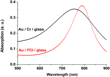
When a metallic chromium seed layer was used to increase the adhesion of Au on glass substrates, it was observed that this Cr layer degrades the LSPR signal.16 Thus, we decided to search for new substrates where no adhesion layer is required and found in the literature19 that ITO substrates are well suited for this purpose. Additionally, the good electrical conductivity of ITO films facilitates sample fabrication by greatly reducing the charging effects during e-beam lithography as well as during size-selected cluster deposition. We utilized commercially available ITO films sputtered onto high-quality float glass substrates (CEC 120 S windows from Präzisions Glas & Optik GmbH). We fabricated Au disks on these commercial substrates using the following parameters: diameter d = 140 nm, height h = 17.5 nm and pitch p = 300 nm. FDTD calculations performed on such Au disks show that on the ITO substrate, the gold disks provide sharper spectra. Fig. 1 shows the simulated optical absorption spectra of the Au disk on bare glass with a Cr layer (black curve) and without any adhesion layer on ITO-coated glass (red curve). The peak obtained with the Cr layer (Au disk/Cr/glass) exhibits a blue-shift (Δλ = −34.4 nm) and is broader (ΔFWHM = +71.2 nm) compared to the Au disk/ITO/glass sample.The choice of ITO substrates therefore offers two main advantages: a conductive substrate, which facilitates e-beam lithography and is required for the deposition of Pt clusters; and a sharper and more intense LSPR signal, which will enhance the sensitivity of our plasmonic sensor.
2.4 Annealing effect
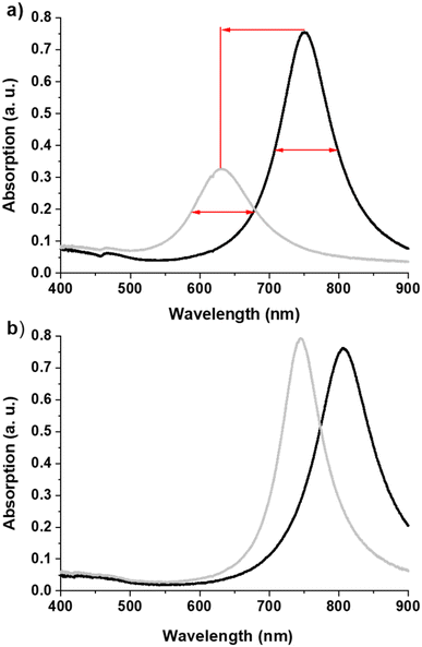
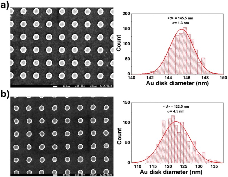
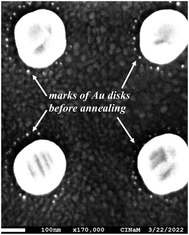
A plasmonic sample (Au disks/ITO/glass) without a SiO2 layer was thermally annealed for 3 h at 350 °C in an oven under a flow of He (250 ml min−1) to stabilize the microstructure and shape of the Au nanodisks.20 This step is important to avoid temperature-induced irreversible spectral shifts during experiments at elevated temperatures, which can be caused by (micro)structural reshaping of the sensor particles. Typically this thermal annealing step leads to the recrystallization of the nanodisks. Fig. 2a shows that annealing induces an increase in FWHM of 20.3 nm and a blue-shift of Δλ = −119.0 nm! It also causes a decrease in the average diameter of the Au disks of 23 nm (Δd = 145.5–122.5) and a shape evolution, as observed by scanning electron microscopy. Fig. 3 shows the SEM images and corresponding diameter distributions before and after annealing. This means that gold material diffuses onto and possibly into the substrate during annealing. Indeed, upon close examination of the high-magnification SEM image (Fig. 4), we observe concentric circles around the annealed Au disks, which are the footprints of the disks before annealing. With FDTD simulations, we cannot solely explain and model such a large blue-shift (Fig. 2a) based on the diameter difference alone. Therefore, we assume that the thickness, roughness and shape of the Au disks are also certainly modified during annealing. Moreover, the optical properties of ITO films can be also modified by annealing as reported by Wu et al.21To minimize such significant modifications, we coated the Au disks on ITO with a SiO2 layer before annealing. In this case (Fig. 2b), the observed blue-shift is smaller (Δλ = −61.8 nm) and the FWHM variation is negative (ΔFWHM = −18.6 nm). This comparison confirms that the SiO2 layer protects and enhances the stability of the detection nanostructure at high temperatures.6 Moreover, CO and oxygen do not absorb on silica layers at temperatures above 35 K, as was already shown by Collings et al. using temperature programmed desorption (TPD).22 Thus, this has no effect on LSPR shift during CO oxidation.
2.5 Pt10 cluster deposition: the LSPR response
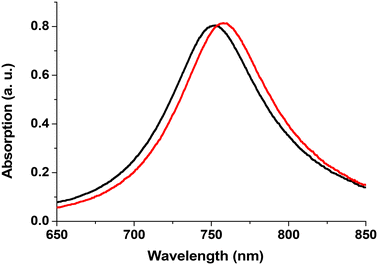
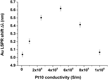
The sample used for Pt cluster deposition consists of Au disks (h = 17.5 nm, p = 300 nm, d = 140 nm) fabricated on a 21 nm thick ITO film on glass, covered with a SiO2 layer (6 nm) and annealed at 350 °C under He flow. We measured LSPR responses before (black points) and after (red points) deposition of Pt10 clusters (Fig. 5) and clearly observed a red-shifted LSPR response of Δλ = 5.8 nm due to the Pt10 clusters.We conducted FDTD simulations [method described in ref. 16] considering the Pt clusters as 2D conductive disks with a thickness of 0.3 nm and a diameter of 1 nm. In our simulations, we considered these 2D objects with a conductivity of 5 × 10⁵ S m−1, which is lower than the bulk conductivity of platinum (9.43 × 10⁶ S m−1). This value is close to that found in the literature for ultrathin Pt films where Agustsson et al.23 measured 5.7 × 10⁵ S m−1 (Fig. 3 of ref. 23) indicating a resistance of 1000 Ω (1 × 10⁻³ S) for a thin film of about 1.75 nm. We also chose a smaller Au disk diameter and thickness (d = 130 nm, h = 15 nm) than the experimental values in an attempt to simulate an annealing effect. We have chosen these values arbitrarily because we don't know exactly what happens during annealing. We certainly have a decrease in the diameter of the Au disks as there is a blue shift in the position of the LSPR response (Fig. 2b), but what about their height? We cannot measure it accurately.
Fig. 6 shows FDTD spectra obtained at different conductivities; the maximum LSPR red-shift (Δλ = 5.6 nm) is obtained at a conductivity of 5 × 10⁵ S m−1. This theoretical shift is in good agreement with the experimental value (Δλ = 5.8 nm measured in Fig. 5).
3. CO and oxygen adsorption and CO oxidation
Gas sensing experiments were conducted in a homemade vacuum (HV) reactor described in detail in ref. 7. Prior to the introduction of CO and O2 gases, the reactor was pumped until a pressure P ≤ 10−6 Pa. We define XCO as the CO molar fraction given by the following equation:| XCO = PCO/(PCO + PO2) | (1) |
3.1 CO adsorption
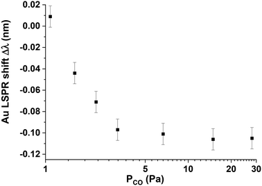
To study CO adsorption, pure gas from Linde (Minican HiQ purity 3.7) was introduced into the HV reactor at T = 418 K at various initial pressures.CO molecules are adsorbed on Pt10 clusters, changing the dielectric properties at the surface of the Pt10 clusters and producing a shift in the LSPR wavelength of the underlying Au disk sensor, this is indirect plasmonic sensing (INPS) because the gold disks are covered with a SiO2 layer and there is no direct contact of gas molecules with Au sensors.7,20 For each CO pressure, we recorded UV-Vis absorption spectra every minute (see Fig. S2†) and we plotted the Au LSPR shift Δλ measured for each CO pressure after t = 30 min when the sample temperature is stabilised (Fig. 7). We could observe a blueshift in the LSPR response, regardless of the initial CO pressure, ranging from 1.1 Pa to 28 Pa. We observed a plateau at approximately Δλ = −0.1 nm at PCO > 2.7 Pa indicating saturation of CO adsorption on Pt10 clusters. This blue-shift is lower than that observed in our previous work on nanometer-size cubic Pt particles.7 If we calculate the number of Pt surface atoms per Au disk, we find that this number is 1.7 times higher for Pt nanocubes than for Pt10 clusters. After successive adsorption measurements, the maximum shift is the same, meaning that there is no coalescence of Pt clusters induced by CO at 418 K. This is in agreement with previous GISAXS measurements showing that coalescence starts at T > 593 K.24
3.2 Oxygen adsorption
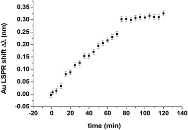
Pure oxygen gas from Linde (Minican HiQ purity 4.5) was introduced into the HV reactor at T = 418 K at PO2 = 87 Pa. We plotted the Au LSPR shift Δλ over time, taking measurements every 5 minutes (Fig. 8).We clearly observed two different regimes during oxygen adsorption: the first with an almost linear Δλ increase (slope = 0.003 nm min−1) and a plateau after 70 min corresponding to a redshift of Δλmax ∼ 0.3 nm which is definitely larger than those measured on 3 nm Pt cubes (Δλmax = 0.2 nm).7 We can therefore assume that we have both oxygen chemisorption and oxidation of Pt10 clusters until reaching a regime where Δλmax remains constant and the Pt10 clusters are fully oxidized. The catalytic activity of Pt clusters depends on their oxidation state, so it's important to monitor this oxidation state and INPS is useful for this purpose. Our result is comparable to the work of Langhammer et al.9 who showed by INPS that oxidation of Pd nanoparticles caused a redshift and a complete oxidation in 100 ppm O2 (corresponding to an O2 partial pressure of 10 Pa at atmospheric pressure). Ono et al.25 studied the interaction of oxygen with Pt nanoparticles (sizes ≤3.6 nm) supported on SiO2/Si(001) and exposed to oxygen plasma at room temperature. From XPS measurements, they show that at low atomic oxygen exposures, chemisorbed species were detected on the samples, whereas higher exposures resulted in complete oxidation of the Pt nanoparticles. Up to 450 K, they found that the content of PtO in the nanoparticles increases, while that of PtO2 decreases, and the metallic Pt remains fairly constant. PtO is stable up to 450 K, after which the decrease in its signal is accompanied by an increase in the metallic Pt content. In addition, for identical atomic oxygen exposures, a decrease in NP size was found to favour their ability to form oxides. C. Dessal et al.26 have followed the possible mobility/redispersion of Pt clusters under O2 by E-STEM under 130 Pa O2. The clusters are quasi-immobile under O2 between RT and 800 °C. DFT calculations show that under these conditions, the Pt13 clusters are strongly oxidized (from 1.5 to 1.8 O per Pt atom) and remain strongly bonded to the support.
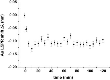
After the oxygen adsorption experiment, the oxygen is evacuated from the reactor kept at 418 K and CO is introduced at a pressure of 44 Pa to try to remove and reduce the oxygen adsorbed on the Pt clusters. In other words, to investigate if the situation was reversible that is to say CO could reduce the oxidized Pt10 clusters, thereby restoring their metallic nature. Fig. 9 shows the evolution of the shift Δλ as a function of time. During the first 10 minutes, Δλ decreases rapidly and finally remains constant at a value of about −0.1 nm. This rapid decrease is explained by the removal of oxygen atoms from the Pt clusters in forming CO2. The minimum value of Δλ after 20 minutes cannot be directly compared with those measured for CO adsorption experiments at PCO saturation (Fig. 7) because the reference values for the shift measurements are not the same. With the clean Pt clusters as a reference, a larger Δλ value is expected. This observation can be understood by two possible explanations: (1) the Pt clusters are not completely reduced after CO exposure and (2) the Pt10 clusters initially 2D become 3D during the reaction of oxygen atoms with CO to form CO2, and as a result, the number of surface Pt atoms decreases, i.e. the maximum number of CO adsorption sites is lower than that for the initial 2D clusters. The second explanation is more likely since a recent report by Yin et al.17 In fact, this work on the CO oxidation of Pt10 clusters on alumina shows (by STM measurements) that there is no coalescence during the reaction, but the initial 2D cluster shape becomes 3D. It is very likely that the same phenomenon occurs for Pt10 supported on silica.
3.3 CO oxidation
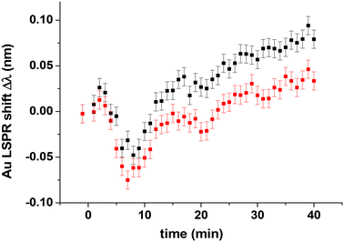
The CO oxidation experiment is performed by introducing a mixture of pure CO and O2 gases with different compositions into the reactor at 418 K, defined by XCO = PCO/(PCO + PO2). The LSPR shifts Δλ induced by the gas upon adsorption/reaction on the Pt10 clusters were measured versus time (Fig. 10).For both XCO values (0.1 and 0.5) given in Fig. 10, we observed a decrease of Δλ and then a linear increase with a slope of 0.003 nm min−1, similar to the slope measured for pure oxygen adsorption (Fig. 8). The two decreases of Δλ during the first 25 minutes can be explained by taking into account Fig. S3,† where we observed that the variation of Δλ is non-linear when the temperature decreases and linear when the temperature increases. So if we subtract the sensitivity (0.02 nm K−1) times the sample temperature variation from the Δλ curve, we still have a negative Δλ variation artefact at t = 7 min and t = 20 min. The final Δλ value (0.08 nm) is greater for XCO = 0.1 (black points) than for XCO = 0.5 (red points), indicating a more oxygen-rich adsorbed layer associated with the lower XCO value. At XCO = 0.5, we measure Δλ = +0.03 nm, superior to the value obtained on Pt nanocubes7 (Δλ = −0.17 nm). This indicates that we are in the O-rich regime on Pt10 clusters, whereas on Pt nanoparticles, we were in the CO-rich regime. This is due to the fact that the CO/Pt10 interaction is weaker than the interaction of CO with 3 nm Pt cubes.
4. Conclusion
The adsorption of CO, oxygen and CO oxidation on size-selected Pt10 clusters were studied by indirect nanoplasmonic sensing (INPS) in the pressure range 1–100 Pa at 418 K. Regarding CO adsorption, we could observe a blueshift in the LSPR response, independent of the initial CO pressure, ranging from 1.1 Pa to 28 Pa. We observed a plateau at approximately Δλ = −0.1 nm at PCO > 2.7 Pa, indicating saturation of CO adsorption on Pt10 clusters. This blue-shift is lower than that observed in our previous work on nanometer-size cubic Pt particles, probably because in Pt10 clusters there are fewer Pt surface atoms per Au disk.For oxygen, we clearly observed two different regimes during oxygen adsorption: the first with an almost linear Δλ increase and a plateau after 70 min corresponding to a redshift of Δλmax ∼ 0.3 nm, which is definitely greater than those measured on 3 nm Pt cubes. We can therefore assume that we have both oxygen chemisorption and oxidation of the Pt10 clusters until we reach a regime where Δλmax remains constant and the Pt10 clusters are completely oxidized. Our results are confirmed by literature work. The catalytic activity of Pt clusters depends on their oxidation state, so it's important to monitor this oxidation state and INPS is useful for this purpose. Demirdjian et al. have shown that chemisorption induces for Pt nanocubes an LSPR blueshift for CO and a redshift for oxygen; they have also shown that this behaviour is correlated with work function measurements found in the literature.7
CO oxidation was performed for XCO = 0.1 and XCO = 0.5, and we observed a decrease of Δλ and then a linear increase, similar to the slope measured for pure oxygen adsorption. The final Δλ value (0.08 nm) is greater for XCO = 0.1 than for XCO = 0.5, indicating a more oxygen-rich adsorbed layer associated with the lower XCO value. At XCO = 0.5, we measured Δλ = +0.03 nm, superior to the value obtained on Pt nanocubes (Δλ = −0.17 nm). This indicates that we are in the O-rich regime on Pt10 clusters, whereas on Pt nanoparticles we were in the CO-rich regime. This is due to the fact that the CO/Pt10 interaction is weaker than the interaction of CO with 3 nm Pt cubes.
This study demonstrates the applicability of indirect nanoplasmonic sensing as a highly sensitive method that allows the study of the adsorption and co-adsorption of CO and O2 on samples with ultrasmall loadings of catalytic metal, here on the example of size-selected Pt10 clusters applied at sub-monolayer coverage, as well as to monitor CO oxidation on these clusters along with the evolution of the oxidation state of Pt and the stability of these particles. This approach opens new ways towards the understanding of the nature and function of matter in the still largely unexplored subnanometer size regime where propensities may abruptly alter after changing the particle size by a single atom.
Data availability
The data supporting this article have been included as part of the ESI.†Conflicts of interest
There are no conflicts to declare.Acknowledgements
Nanofabrication processes were performed in the PLANETE cleanroom facility (CINaM, Marseille), a part of the Renatech + French National network.The authors sincerely thank the laboratory electron microscopy service and its agents (A. Altié and D. Chaudanson) for assisting them in SEM observations.
M. V. and S. V. acknowledge the assistance provided by the Advanced Multiscale Materials for Key Enabling Technologies project, supported by the Ministry of Education, Youth, and Sports of the Czech Republic. Project No. CZ.02.01.01/00/22_008/0004558, co-funded by the European Union. M. V. and S. V. would like to thank the Argonne National Laboratory for facilitating the use of the cluster synthesis equipment for this study.
References
- C. R. Henry, Surf. Sci. Rep., 1998, 31, 235–326 CrossRef.
- G. A. Somorjai, R. L. York, D. Butcher and J. Y. Park, Phys. Chem. Chem. Phys., 2007, 9, 3500–3513 RSC.
- E. Ozensoy, D. C. Meier and D. W. Goodman, J. Phys. Chem. B, 2002, 106, 9367–9371 CrossRef CAS.
- J. Wang, A. Ouvrard, W. Zheng, S. Carrrez, A. Ghalgaoui and B. Bourguignon, Phys. Chem. Chem. Phys., 2023, 25, 10845–10852 RSC.
- L. Nguyen, F. F. Tao, Y. Tang, J. Dou and X. J. Bao, Chem. Rev., 2019, 119, 6822–6905 CrossRef PubMed.
- E. M. Larsson, C. Langhammer, I. Zoric and B. Kasemo, Science, 2009, 326, 1091–1094 CrossRef CAS PubMed.
- B. Demirdjian, I. Ozerov, F. Bedu, A. Ranguis and C. R. Henry, ACS Omega, 2021, 6, 13398–13405 CrossRef CAS PubMed.
- C. Langhammer, E. M. Larsson, B. Kasemo and I. Zoric, Nano Lett., 2010, 10, 3529–3538 CrossRef CAS PubMed.
- C. Langhammer and E. M. Larsson, ACS Catal., 2012, 2, 2036–2045 CrossRef CAS.
- S. Liu, A. Susarrey-Arce, S. Nilsson, D. Albinsson, L. Hellberg, S. Alekseeva and C. Langhammer, ACS Nano, 2019, 13, 6090–6100 CrossRef CAS PubMed.
- K. Wettergren, A. Hellman, F. Cavalca, V. P. Zhdanov and C. Langhammer, Nano Lett., 2015, 15, 574–580 CrossRef CAS PubMed.
- E. C. Tyo and S. Vajda, Nat. Nanotechnol., 2015, 10, 577–588 CrossRef CAS PubMed.
- R. Jin, G. Li, S. Sharma and Y. Li, Chem. Rev., 2021, 121, 567–648 CrossRef CAS PubMed.
- N. Zaman, G. Roberts, J. von der Heyde and A. Kara, Surf. Sci., 2023, 733, 122290 CrossRef CAS.
- S. Nigam and C. Majumder, Appl. Surf. Sci., 2021, 547, 149160 CrossRef CAS.
- B. Demirdjian, I. Ozerov, F. Bedu, A. Ranguis and C. R. Henry, Chem. Phys. Lett., 2024, 837, 141063 CrossRef CAS.
- C. Yin, F. R. Negreiros, G. Barcaro, A. Beniya, L. Sementa, E. C. Tyo, S. Bartling, K.-H. Meiwes-Broer, S. Seifert, H. Hirata, N. Isomura, S. Nigam, C. Majumder, Y. Watanabe, A. Fortunelli and S. Vajda, J. Mater. Chem. A, 2017, 5, 4923–4931 RSC.
- C. Yin, E. Tyo, K. Kuchta, B. von Issendorff and S. Vajda, J. Chem. Phys., 2014, 140, 174201 CrossRef CAS PubMed.
- I. Ragheb, M. Braik, S. Lau-Truong, A. Belkhir, A. Rumyantseva, S. Kostcheev, P. M. Adam, A. Chevillot-Biraud, G. Levi, J. Aubard, L. Boubekeur-Lecaque and N. Felidj, Nanomaterials, 2020, 10, 2201 CrossRef CAS PubMed.
- C. Langhammer, E. M. Larsson, B. Kasemo and I. Zoric, Nano Lett., 2010, 10, 3529–3538 CrossRef CAS PubMed.
- W.-F. Wu and B.-S. Chiou, Appl. Surf. Sci., 1993, 68, 497–504 CrossRef CAS.
- M. P. Collings, V. L. Frankland, J. Lasne, D. Marchione, A. Rosu-Finsen and M. R. S. McCoustra, Mon. Not. R. Astron. Soc., 2015, 449, 1826–1833 CrossRef CAS.
- J. S. Agustsson, U. B. Arnalds, A. S. Ingason, K. B. Gylfason, K. Johnsen, S. Olafsson and J. T. Gudmundsson, J. Phys.: Conf. Ser., 2008, 100, 082006 CrossRef.
- R. E. Winans, S. Vajda, B. Lee, S. J. Riley, S. Seifert, G. Y. Tikhonov and N. A. Tomczyk, J. Phys. Chem. B, 2004, 108, 18105–18107 CrossRef CAS.
- L. K. Ono, J. R. Croy, H. Heinrich and B. R. Cuenya, J. Phys. Chem. C, 2011, 115, 16856–16866 CrossRef CAS.
- C. Dessal, A. Sangnier, C. Chizallet, C. Dujardin, F. Morfin, J.-L. Rousset, M. Aouine, M. Bugnet, P. Afanasiev and L. Piccolo, Nanoscale, 2019, 11, 6897–6904 RSC.
Footnote |
| † Electronic supplementary information (ESI) available. See DOI: https://doi.org/10.1039/d4nr02682a |
| This journal is © The Royal Society of Chemistry 2024 |

