 Open Access Article
Processing of a P(NDI2OD-T2) film without an intermediate wetting layer during spin-coating to improve charge carrier mobility†
Sichun
Wang
ab,
Junhang
Li
ac,
Xinyu
Liu
ac,
Qiang
Zhang
a,
Xinhong
Yu
a and
Yanchun
Han
 *ac
*ac
aState Key Laboratory of Polymer Physics and Chemistry, Changchun Institute of Applied Chemistry, Chinese Academy of Sciences, Changchun, 130022, P. R. China. E-mail: ychan@ciac.ac.cn
bLaboratory of Molecular Materials and Devices, Department of Materials Science, Fudan University, 200433 Shanghai, P. R. China
cSchool of Applied Chemistry and Engineering, University of Science and Technology of China, Hefei, 230026, P. R. China
First published on 24th September 2024
Abstract
The thin film morphology of a conjugated polymer is one of the important factors in determining its electrical performance, which is controlled by thermodynamic and kinetic factors. However, attaining a clear solution processing window for film preparation remains challenging due to the intrinsic complex properties of polymers and solvents. Herein, we proposed a strategy to obtain a uniform fibrous morphology by direct formation of conjugated polymer films on a substrate without an intermediate wetting layer via controlling solvent evaporation. We chose a poly{[N,N′-bis(2-octyldodecyl)-naphthalene-1,4,5,8-bis(dicarboximide)-2,6-diyl]-alt-5,5′-(2,2′-bithiophene)} [P(NDI2OD-T2)] solution as the model system. The intermediate wetting layer vanishes during the spin-coating deposition when the solvent evaporation speed is greater than 130–140 μm s−1 achieved by increasing the substrate temperature. At this point, in the time-resolved in situ photoluminescence (PL) spectra of P(NDI2OD-T2), an intermediate transition state of the 0–1 peak appears at 756 nm in addition to the 0–0 peak at 834 nm. This indicates that the polymer chains are rearranged to form homogeneous fibers without detrimental aggregation. Compared to the film formed with an intermediate wetting layer, some large aggregates can be observed. Thus, the electron mobility reaches 0.33 ± 0.02 cm2 V−1 s−1 for the film without the intermediate wetting layer, which is 3 times higher than that of the film formed with the wetting layer. The relationship between the deposition regimes, microstructure and charge carrier mobility was also revealed in other solvents, which can serve as generalized guidelines for conjugated polymer film deposition.
Introduction
Conjugated semiconductor polymers are considered promising candidates in electronic devices due to their solution processability, mechanical flexibility and tunable optoelectronic properties.1–3 The electrical properties of these polymers are dependent on the final film morphology.4–6 However, owing to the effects of the molecular structure,7–10 solvent properties,11–13 processing method,14–17etc., the film morphology is highly sensitive to thermodynamic and kinetic processes. It always takes a lot of effort to identify optimal processing conditions for a specific polymer, thereby significantly hindering its broader application potential.18,19 Therefore, understanding the relationship between the thin film deposition process and the electrical performances of devices is crucial for providing a clear solution processing window for film preparation.The solution processing window is divided into the Landua–Levich (LL) regime and the solvent evaporation regime in meniscus-guided coating.20,21 The intermediate wetting layer is pulled out and then dried into films in the LL regime. In contrast, the film is directly dry and does not undergo the intermediate wetting layer stage in the solvent evaporation regime because of the fast solvent evaporation speed.22,23 Our previous work has shown that film formation during critical solvent evaporation is beneficial for the final film morphology and electrical performance when using blade coating.24 Spin-coating is one of the most widespread and efficient solution processing protocols, which is also significantly affected by the solvent evaporation speed during processing. Thus, the relationship between the solvent evaporation speed and the film formation process should be further explored. Janneck et al.25 proposed a model for the relationship between the solvent evaporation speed and substrate temperature, expressed by the following equation:
Ve = AVMT0.7![[thin space (1/6-em)]](https://www.rsc.org/images/entities/char_2009.gif) exp(−(ΔSvap)/RTb/T) exp(−(ΔSvap)/RTb/T) | (1) |
To explore the optimal conditions for film deposition, it is imperative to delineate the thermodynamic and kinetic processes in film formation drying.27–30 In recent years, the drying behaviour of polymer solutions during processing has been tracked to monitor and better understand film formation mechanisms.31,32 This was achieved by controlling and systematically changing processing conditions, such as the atmosphere,33 solvent,34–36 or temperature.37 In particular, in terms of temperature, at a higher temperature and a faster solvent drying speed, with all other factors remaining constant, the film formation process was accelerated.32 Furthermore, as the temperature increases, the film-forming process transforms from crystal nucleation dominated to crystal growth dominated, and the changes in crystallization behaviour lead to various film morphologies.38 Only thin films prepared at a suitable temperature show the optimal morphology and device mobility.39 Therefore, the optimal film formation conditions require further exploration.
P(NDI2OD-T2) has been widely studied as a classical n-type D–A conjugated polymer.40–43 Previous studies have reported a proficient method to regulate the solidification speed of P(NDI2OD-T2), enabling kinetically controlled crystallization processes at various temperatures. A suitable solidification speed is beneficial for the nucleation and growth of crystals and to obtain large-sized crystal domains. The OFET device mobility increased from 0.04 to 3.43 cm2 V−1 s−1.44 However, the optimal film-forming conditions required for different study systems vary, mainly due to the complex properties of polymers and solvents.24,45 Thus, it is necessary to investigate in depth the relationship between the optimal range of solvent evaporation rates and electrical performance to optimize the film fabrication technology.
In this study, we have revealed that thin films have a more uniform fibrous morphology and better electrical performance if they are directly dry without undergoing the intermediate wetting layer during the deposition process. The intermediate wetting layer disappears during the spin-coating process as the increase in substrate temperature accelerates the solvent evaporation speed. Owing to the enhanced polymer chain motility induced by the thermodynamic and kinetic factors, the polymer chains are rearranged and favour the formation of homogeneous fibres. Therefore, the electron mobility has been improved 3-fold compared to that of the film formed with the intermediate wetting layer. Exploring the deposition process of conjugated polymer films provides theoretical guidance for further optimizing the solution processing technology.
Experimental section
Materials and solvents
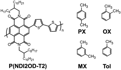
Poly{[N,N′-bis(2-octyldodecyl)-naphthalene-1,4,5,8-bis(dicarboximide)-2,6-diyl]-alt-5,5′-(2,2′-bithiophene)} [P(NDI2OD-T2)] was purchased from 1-Material in Canada. The weight average molecular weight (Mw) was 171 kDa, and the molecular weight dispersity (Đ) was 3.0. The solvents o-xylene (OX), m-xylene (MX), and p-xylene (PX) were purchased from Beijing Chemical Factory, and toluene (Tol) was purchased from Sigma Aldrich. The chemical structures of the polymer and solvents are shown in Scheme 1.Sample preparation
A P(NDI2OD-T2) solution was prepared at a concentration of 5 mg mL−1 in solvents Tol, OX, MX and PX, respectively, and then heated for 4 hours to ensure complete dissolution. The four solvents were chosen for two reasons: (1) they are all solvents that selectively dissolve the side chains of P(NDI2OD-T2) and favor orderly aggregation in solution and (2) the toxicity of aromatic solvents is less than that of halogen solvents. For film preparation, silicon wafers covered with 300 nm thick silicon dioxide were employed as substrates. The wafers were sonicated with deionized water, acetone and isopropanol for 15 min. The substrates were held in a thermal spin coater until they reached the specified temperature. To obtain the films, 15 μL of the solution was spin-dropped using a transfer liquid gun and the rotational speed was 2000 rpm. The film thickness was about 30 nm, and the specific thickness value is shown in Table S1.†Characterization
The fluorescence (PL) spectra were recorded using a miniature optical fibre spectrometer with a LIFS-405 series laser-induced fluorescence system (a 405 nm solid-state laser was selected as the excitation source). The fibre probe was an FPB-405-1.5-SS from China. The data were collected using Ocean Optics software. Peak intensities as a function of film formation time were recorded using in situ PL spectra at a time interval of 0.01 s. The in situ PL spectra were recorded at a time interval of 0.05 s for the specified wavelength. The low-magnification film morphology images were captured using a JEM-1400 (JEOL, Japan) operated at 120 kV. Cryogenic transmission electron microscopy (cryo-TEM) images were obtained using a JEM-3200FSC (JEOL, Japan) operated at 300 kV and −180 °C. The sample preparation involved exposure to hydrofluoric acid vapor for 10 s. Subsequently, the film was immersed in deionized water to make it fall off and then carefully collected onto copper grids for further characterization. The copper grids (AZH300) for TEM tests were purchased from Beijing Zhongjingkeyi Technology Co., Ltd. The copper grids covered with holey carbon films (R 2/2) for cryo-TEM were purchased from Quantifoil. The small angle X-ray scattering (SAXS) and grazing incidence wide-angle X-ray scattering (GIWAXS) data of solid-state films were collected at the 1W1A X-ray scattering station, Beijing Synchrotron Radiation Facility. The incidence angle was 0.2°, the wavelength of the beamline was 1.54 Å, and the exposure time was 30 s. SasView software facilitated the analysis of the SAXS data, wherein one-dimensional (1D) profiles were derived by interrailing the signal along the qxy direction of scattering images. Regarding GIWAXS, a two-dimensional image plate detector, an EIGERX 1M from DECTRIS in Switzerland, was employed to capture the diffraction images.Device fabrication and measurements
The electrical performances were determined using organic field-effect transistors (OFETs) with a bottom-gate top-contact (BGTC) architecture. Highly doped n-type silicon with a 300 nm silicon dioxide layer was used as substrates. These substrates were ultrasonically cleaned with deionized water, acetone, and isopropanol, each for 5 min, followed by ultraviolet ozone treatment for 25 min. Substrate surface modification was achieved through octadecyltrichlorosilane (OTCS, Sigma-Aldrich). This involved mixing 1.3 μL OTCS with 1.0 μL trichloroethylene (Beijing Chemical Factory) and then performing a spin-coating process at 3000 rpm for 30 s. Thereafter, the treated substrates were placed within a desiccator with an ammonia atmosphere for 8 hours. Then, the modified wafers were washed with toluene for 3 min and dried under a N2 flow. After the film deposition, the source and drain electrodes were fabricated by evaporating gold in a vacuum environment, maintaining a channel width (W) to length (L) ratio of 5, width = 1000 μm, and L = 200 μm. Ultimately, the electrical performance of P(NDI2OD-T2)-based OFETs, including output (IDS–VDS) and transfer (IDS–VGS) curves, was measured through a Keysight B1500A semiconductor device analyzer.Results and discussion
Thin film deposition process during spin coating
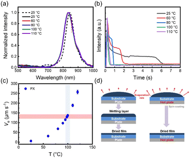
The conjugated polymer film morphology is the result of an interplay of processes, especially the thermodynamics and kinetics of solidification. To explore the film deposition process, the P(NDI2OD-T2) from the solution state to the film state was monitored using in situ PL spectroscopy. First, the in situ monitoring signal peaks at different substrate temperatures were calibrated by photoluminescence (PL) spectroscopy, as shown in Fig. 1(a). The film exhibited a single peak at 834 nm, and the intensity of the characteristic peak was monitored as a function of the film formation time. Consequently, the film drying process as a function of drying time at different substrate temperatures is shown in Fig. 1(b). With solvent evaporation, the characteristic peak intensity gradually decreases. Interestingly, the intensity of the characteristic peaks decreases to a certain extent and then a plateau period appears with constant intensity at room temperature. Among them, the plateau indicates that the solution forms a wetting layer upon spin-coating, which lasts approximately 3.5 s. In the presence of the wetting layer, we considered that the viscous force imparted by the substrate is dominant in the film-forming process. Subsequently, the intensity continued to decrease gradually at approximately 5.4 s. Eventually, the intensity of the characteristic peaks reaches a stable state, and the whole film formation time is about 6.5 s. However, as the substrate temperature increases, the time of film formation and the plateau period also decrease. When the substrate temperature is 80 °C, the whole film-forming process takes about 1 s and a plateau of the characteristic peak intensity also appears for a short period of time, and then the wetting layer dries into a thin film. In contrast, when the substrate temperature increases to 100 °C and 110 °C, it can be found that the plateau period of the peak intensity disappears. The intensity of the characteristic peaks decreases rapidly to an unchanging state. This indicates that the film is formed directly without the intermediate wetting layer during the spin coating process. Therefore, we proposed that the film formation with or without an intermediate wetting layer was mainly determined by solvent evaporation. The solvent evaporation speed can be controlled through the substrate temperature. For P(NDI2OD-T2) in PX solvent, the critical substrate temperature for the disappearance of the intermediate wetting layer was 100 °C (Fig. 1(b)). Moreover, the solvent evaporation speed was calculated using the model proposed by Janneck et al.,25 as shown in Fig. 1(c) and Table S2.† As the substrate temperature increases, the solvent evaporation speed also becomes progressively faster. The critical solvent evaporation speed of the intermediate wetting layer disappearance was 137 μm s−1. Below the critical evaporation rate, an intermediate wetting layer stage was generated during the film deposition. In contrast, the wetting layer disappeared above the critical evaporation speed. The schematic diagram is shown in Fig. 1(d). Their major difference is whether there is an intermediate wetting layer during the film deposition process.To obtain kinetic information on the film-forming process, we recorded the time-resolved in situ PL spectra of P(NDI2OD-T2) at different deposition temperatures. The device schematic diagram of in situ PL absorption spectroscopy is shown in Fig. 2(a). The temporal evolution process from the solution state to the solid state film is shown in Fig. 2(b–f). The film formation time gradually shortened as the substrate temperature increased. Throughout the film formation process, regardless of the substrate temperature, the intensity of the PL peak exhibits a time-dependent increase reaching a maximum midway, a sweet spot in aggregate concentration that maximizes the number of emissive aggregates.37 Then, as the solvent further evaporates, the intensity gradually decreases before levelling off. However, at low deposition temperatures, the evolution process from the solution state to the solid state film exhibits only a single peak of 0–0 at 834 nm. With the accelerated evaporation speed, an intermediate state of the 0–1 peak appears at 756 nm in addition to the 0–0 peak, followed by the disappearance of the 0–1 peak, and the final film also shows a 0–0 single peak at 100 °C and 110 °C. It is attributed to the enhanced polymer chain motility induced by the elevated temperature. The appearance of the 0–1 peak intermediate state indicates polymer chain rearrangement during the film formation, which favours the ordering of the final state film and promotes charge transport.
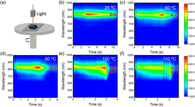 | ||
| Fig. 2 (a) Schematic diagram of the in situ PL absorption spectroscopy device. (b–f) Time-dependent PL spectra of P(NDI2OD-T2) films at various substrate temperatures, respectively. | ||
Morphology of P(NDI2OD-T2) films at different substrate temperatures
To further explore the effects of various film deposition processes on the microstructure at different substrate temperatures, we characterized the film morphology using a transmission electron microscope (TEM), as shown in Fig. 3(a–e). Island aggregates and small-sized fibres were formed with a fibrous length of about 90 nm and a fibrous width of about 4.2 nm at 25 °C substrate temperature. As the substrate temperature increases, the island aggregates gradually decrease. When the substrate temperature reaches 100 °C, the aggregates disappear. The film morphology was uniform and the fibrous size increased to an average length of about 185 nm and a width of about 9.8 nm. The specific values of the fibrous length and width are shown in Table S3.† The optimization of the film morphology facilitates charge transport. The morphology on the molecular chain scale was further characterized using cryo-TEM at 100k magnification, as shown in Fig. 3(f–j). The observed striped patterns represented orderly arranged molecular chain crystal lattices, and an increase in the size of the crystalline region was also attained.However, upon elevating the substrate temperature to 110 °C, a gray pattern with different shades appeared at the nanoscale due to fast solvent evaporation, indicating significant inhomogeneity.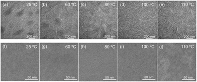 | ||
| Fig. 3 TEM images of the P(NDI2OD-T2) films at various substrate temperatures. (a–e) Low-magnification images (30k) and (f–j) high-magnification images (100k). | ||
Moreover, the films within a small range of structural features were further investigated by SAXS. The scattering patterns and profiles are depicted in Fig. S1† and Fig. 4(a–e), and the domain size was obtained from model fitting, as shown in Fig. 4(f). With the increase in substrate temperature, the domain size of P(NDI2OD-T2) films gradually increased from 24.9 nm to 34.0 nm. Notably, the domain sizes obtained by SAXS represent a nanoscale crystalline phase, while the fibrous length and width measured by TEM reflect the microstructural morphology of the film, comprising an ensemble of crystalline and amorphous regions. Due to differences in the test scale and observation methods, the size increase in SAXS is smaller than the enlargement of the fibrous length as measured by TEM. Nevertheless, regardless of the characterization technique, the size gradually increases with the increasing substrate temperature. It is well known that matching the crystallization rate with the solvent evaporation speed can facilitate the formation of large-sized domains. Herein, the relatively high substrate temperature provides sufficient thermal energy for crystal growth to accommodate the film formation process. Therefore, a large crystallization domain was attained, which may promote interchain charge transport.
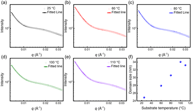 | ||
| Fig. 4 (a–e) Representative SANS data fitted for P(NDI2OD-T2) films at various substrate temperatures with the cylinder model. (f) Fitted domain size as a function of substrate temperatures. | ||
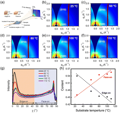
To reveal the molecular orientation arrangement of the films, detailed molecular packing was carried out using GIWAXS characterization. The schematic diagram of the 2D GIWAXS device is shown in Fig. 5(a). 2D GIWAXS images are shown in Fig. 5(b–f). Two diffraction peaks (010) and (100) are shown in the out-of-plane direction and (100) diffraction peaks in the in-plane direction, indicating the coexistence of face-on and edge-on orientations. For quantifying molecular orientation details, we determined the proportions of face-on and edge-on orientations by examining changes in the (100) peak intensity with respect to the azimuthal angle (χ). Specifically, angles ranging from 0° to 45° were classified as indicative of edge-on orientation, whereas those from 45° to 90° were attributed to face-on orientation13 (Fig. 5(g)). Through the integration of the respective peak areas, the contents of edge-on and face-on oriented crystallites are quantized, as depicted in Fig. 5(h). Notably, at a substrate temperature of 25 °C, the content of edge-on oriented crystallites surpassed that of the face-on oriented crystallites. With the substrate temperature increasing, the face-on oriented crystallite content gradually increased and dominated. This is due to the edge-on orientation being a stable orientation of P(NDI2OD-T2),46 however, the rapid film formation failed to reach a steady state, and thus the film tended to adopt a face-on crystallite arrangement.
The electrical performances of P(NDI2OD-T2) films
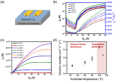
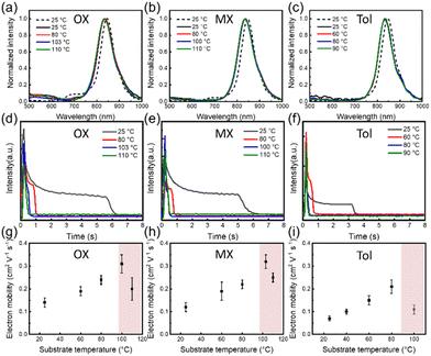
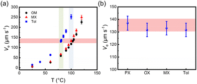
Electrical performances are closely associated with the deposition kinetics and film microstructure. To characterize the electrical performances of P(NDI2OD-T2) thin films, we fabricated OFETs with a bottom-gate top-contact structure as shown in Fig. 6(a) and measured the corresponding electron mobility. Fig. 6(b and c) show the transfer and output characteristic curves for devices fabricated under varying film deposition conditions. Consequently, the electron mobility values are derived from the saturation regions as presented in Fig. 6(d). As the substrate temperature increased, the electron mobility of the films showed a trend of first increasing and then decreasing. The optimal electrical performance was obtained at a substrate temperature of 100 °C, and the corresponding average charge carrier mobility is 0.33 ± 0.02 cm2 V−1 s−1, coinciding with the disappearance of the intermediate wetting layer. In this case, the polymer chains are rearranged to form homogeneous fibres without detrimental aggregation. Moreover, the domain and fibrous size increase, as characterized by SANS and TEM. All these contribute to the improved electrical performance. However, further increasing the substrate temperature resulted in heterogeneous films, which was detrimental to the electrical performance.To gain a deeper understanding of the solution processing window, the correlation of the deposition processes should be examined in other solvents, for example, OX, MX and Tol. Similarly, the PL spectra of the solution and the film are shown in Fig. 7(a–c), and all film spectra showed signal peaks between 830 and 835 nm. These characteristic signal peak positions were used to monitor the film formation process at various substrate temperatures, as shown in Fig. 7(d–f). The characteristic peak intensity gradually decreased as the solvent evaporated. An intermediate wetting layer was formed during spin-coating at low substrate temperature. As the substrate temperature increases, the wetting layer gradually disappears. The critical substrate temperatures for the disappearance of the intermediate wetting layer are 103 °C, 100 °C and 80 °C, respectively. The electrical performances at different substrate temperatures were also investigated, and the representative output and transfer curves are shown in Fig. S2.† In Fig. 7(g–i), the optimal electron mobility was attained at the critical evaporation temperature, where the wetting layer disappeared regardless of the solvents. The corresponding optimal average electron mobility values were 0.32 ± 0.03 cm2 V−1 s−1, 0.31 ± 0.04 cm2 V−1 s−1, and 0.21 ± 0.03 cm2 V−1 s−1, respectively. Therefore, based on the relationship between film deposition conditions and electrical performance, we found that the optimum charge carrier mobility was obtained in the intermediate wetting layer disappearance process. Furthermore, we also evaluated the solvent evaporation speed for different solvents at various substrate temperatures as shown in Tables S4–S6† and Fig. 8(a). Interestingly, the evaporation speeds at the temperature of the intermediate wetting layer disappearance were all in the range of 130–140 μm s−1 regardless of solvents, as shown in Fig. 8(b). Therefore, we speculate that evaporation speeds in this range could lead to the disappearance of the intermediate wetting layer and provide optimal electrical performance.
Conclusions
In summary, we revealed the relationship between the film spin coating deposition process, morphology and electrical performances. Thin films have a more uniform fibre morphology and optimal electrical performance if they are directly dry without undergoing the intermediate wetting layer during the deposition process. The critical evaporation speeds of the intermediate wetting layer disappearance were all in the range of 130–140 μm s−1 regardless of the solvents. Furthermore, through in situ PL spectral characterization, we confirmed that the films are subjected to a polymer chain rearrangement process during film formation without the intermediate wetting layer. The improved film uniformity is beneficial for enhanced charge carrier mobility. The relationship between the film deposition process, microstructure and electrical performance was also revealed in other solvents, which can serve as generalized guidelines for conjugated polymer film deposition.Author contributions
S. W.: data curation, formal analysis, investigation, validation, visualization, writing – original draft and writing – review & editing. J. L.: formal analysis, investigation and visualization. X. L.: methodology and formal analysis. Q. Z.: supervision and writing – review & editing. X. Y.: supervision, project administration and writing – review & editing. Y. H.: conceptualization, funding acquisition, project administration, supervision and writing – review & editing.Data availability
The data supporting this article have been included as part of the ESI† and are available from the authors on request.Conflicts of interest
There are no conflicts to declare.Acknowledgements
This work was partly supported by the National Natural Science Foundation of China (52433009 and 51933010) and the Strategic Priority Research Program of the Chinese Academy of Sciences (Grant No. XDB 0520000).References
- Z. Ding, D. Liu, K. Zhao and Y. Han, Macromolecules, 2021, 54, 3907–3926 CrossRef CAS.
- K. Q. Liu, Y. H. Gu, Z. R. Yi and Y. Q. Liu, Chin. J. Polym. Sci., 2023, 41, 671–682 CrossRef CAS.
- M. Kim, S. U. Ryu, S. A. Park, K. Choi, T. Kim, D. Chung and T. Park, Adv. Funct. Mater., 2019, 30, 1904545 CrossRef.
- Z. F. Yao, J. Y. Wang and J. Pei, Prog. Polym. Sci., 2023, 136, 101626 CrossRef CAS.
- K. S. Park, J. J. Kwok, P. Kafle and Y. Diao, Chem. Mater., 2021, 33, 469–498 CrossRef CAS.
- X. Cao and Y. Han, Aggregate, 2024, 5, e501 CrossRef CAS.
- S. Ren, Z. Wang, W. Zhang, A. Yassar, J. Chen and S. Wang, Molecules, 2024, 29, 260 CrossRef CAS.
- S. Ren, Z. Wang, J. Chen, S. Wang and Z. Yi, Molecules, 2024, 29, 457 CrossRef CAS.
- S. Ren, S. Wang, J. Chen and Z. Yi, Polymers, 2024, 16, 396 CrossRef CAS.
- X. Yuan, H. Chen, S. Kim, Y. Chen, Y. Zhang, M. Yang, Z. Chen, C. Yang, H. Wu, X. Gao, Z. Liu and C. Duan, Adv. Energy Mater., 2023, 13, 2204394 CrossRef CAS.
- L. Zhang, H. Li, K. Zhao, T. Zhang, D. Liu, S. Wang, F. Wu, Q. Zhang and Y. Han, Polymer, 2023, 275, 125912 CrossRef CAS.
- T. Zhang, Y. Liu, L. Zhang, S. Wang, J. Li, J. Zuo, X. Yu, Q. Zhang and Y. Han, J. Mater. Chem. C, 2023, 11, 2302–2315 RSC.
- H. Li, H. Yang, L. Zhang, S. Wang, Y. Chen, Q. Zhang, J. Zhang, H. Tian and Y. Han, Macromolecules, 2021, 54, 10557–10573 CrossRef CAS.
- K. Choudhary, A. X. Chen, G. M. Pitch, R. Runser, A. Urbina, T. J. Dunn, M. Kodur, A. T. Kleinschmidt, B. G. Wang, J. A. Bunch, D. P. Fenning, A. L. Ayzner and D. J. Lipomi, ACS Appl. Mater. Interfaces, 2021, 13, 51436–51446 CrossRef CAS.
- Y. Minowa, Y. Yabuuchi, S. Nagano, S. Nagamatsu, A. Fujii and M. Ozaki, ACS Appl. Mater. Interfaces, 2022, 14, 50112–50119 CrossRef CAS.
- Y. Zhang, B. Wu, Y. He, W. Deng, J. Li, J. Li, N. Qiao, Y. Xing, X. Yuan, N. Li, C. J. Brabec, H. Wu, G. Lu, C. Duan, F. Huang and Y. Cao, Nano Energy, 2022, 93, 106858 CrossRef CAS.
- X. Tan, Y. Li, X. Yuan, S. Kim, Y. Zhang, C. Yang, F. Huang, Y. Cao and C. Duan, Sci. China: Chem., 2023, 66, 2347–2353 CrossRef CAS.
- Z. Xu, K. S. Park, J. J. Kwok, O. Lin, B. Patel, P. Kafle, D. W. Davies, Q. Chen and Y. Diao, Adv. Mater., 2022, 34, e2203055 CrossRef PubMed.
- L. Tang, L. Thomsen and C. R. McNeill, ACS Appl. Polym. Mater., 2022, 4, 5501–5514 CrossRef.
- B. B. Patel and Y. Diao, Nanotechnology, 2018, 29, 044004 CrossRef PubMed.
- X. Gu, L. Shaw, K. Gu, M. F. Toney and Z. Bao, Nat. Commun., 2018, 9, 534 CrossRef PubMed.
- Z. Lu, C. Wang, W. Deng, M. T. Achille, J. Jie and X. Zhang, J. Mater. Chem. C, 2020, 8, 9133–9146 RSC.
- K. S. Park, J. J. Kwok, R. Dilmurat, G. Qu, P. Kafle, X. Luo, S. H. Jung, Y. Olivier, J. K. Lee, J. Mei, D. Beljonne and Y. Diao, Sci. Adv., 2019, 5, eaaw7757 CrossRef CAS PubMed.
- S. Wang, H. Li, K. Zhao, L. Zhang, Q. Zhang, X. Yu, H. Tian and Y. Han, Macromolecules, 2022, 55, 2497–2508 CrossRef CAS.
- R. Janneck, F. Vercesi, P. Heremans, J. Genoe and C. Rolin, Adv. Mater., 2016, 28, 8007–8013 CrossRef CAS PubMed.
- M. Chen, B. Peng, S. Huang and P. K. L. Chan, Adv. Funct. Mater., 2019, 30, 1905963 CrossRef.
- S. Wang, T. Zhang, L. Zhang, D. Liu, X. Liu, J. Li, H. Li, Q. Zhang and Y. Han, Polymer, 2022, 262, 125435 CrossRef CAS.
- O. Urquidi, J. Brazard, N. LeMessurier, L. Simine and T. B. M. Adachi, Proc. Natl. Acad. Sci. U. S. A., 2022, 119, e2122990119 CrossRef CAS PubMed.
- E. F. Manley, J. Strzalka, T. J. Fauvell, T. J. Marks and L. X. Chen, Adv. Energy Mater., 2018, 8, 1800611 CrossRef.
- L. J. Richter, D. M. DeLongchamp and A. Amassian, Chem. Rev., 2017, 117, 6332–6366 CrossRef CAS PubMed.
- S. J. Rinehart, G. Yuan and M. D. Dadmun, Macromolecules, 2018, 51, 7836–7844 CrossRef CAS.
- M. Buchhorn, S. Wedler and F. Panzer, J. Phys. Chem. A, 2018, 122, 9115–9122 CrossRef CAS PubMed.
- S. Pröller, D. Moseguí González, C. Zhu, E. Schaible, C. Wang, P. Müller-Buschbaum, A. Hexemer and E. M. Herzig, Rev. Sci. Instrum., 2017, 88, 066101 CrossRef PubMed.
- Y. J. Kim, S. Lee, M. R. Niazi, K. Hwang, M. C. Tang, D. H. Lim, J. S. Kang, D. M. Smilgies, A. Amassian and D. Y. Kim, ACS Appl. Mater. Interfaces, 2020, 12, 36417–36427 CrossRef CAS.
- J. Chang, B. Sun, D. W. Breiby, M. M. Nielsen, T. I. Solling, M. Giles, I. McCulloch and H. Sirringhaus, Chem. Mater., 2004, 16, 4772–4776 CrossRef CAS.
- T. Kassar, N. S. Güldal, M. Berlinghof, T. Ameri, A. Kratzer, B. C. Schroeder, G. L. Destri, A. Hirsch, M. Heeney, I. McCulloch, C. J. Brabec and T. Unruh, Adv. Energy Mater., 2016, 6, 1502025 CrossRef.
- F. Panzer, M. J. Dyson, H. Bakr, S. Wedler, K. Schötz, M. Chauhan, P. N. Stavrinou, A. Köhler and N. Stingelin, Adv. Funct. Mater., 2024, 2314729 CrossRef.
- Y. Yan, R. Zhang, Q. Liang, J. Liu and Y. Han, Polymer, 2019, 182, 121827 CrossRef.
- H. Li, X. Liu, T. Jin, K. Zhao, Q. Zhang, C. He, H. Yang, Y. Chen, J. Huang, X. Yu and Y. Han, Macromol. Rapid Commun., 2022, 43, e2200084 CrossRef.
- X. Liu, Y. Yan, Q. Zhang, K. Zhao and Y. Han, Chem. Res. Chin. Univ., 2021, 37, 1019–1030 CrossRef CAS.
- D. Vu, W. L. Tan, L. He, A. Ehm, D. R. T. Zahn and C. R. McNeill, ACS Macro Lett., 2023, 12, 140–146 CrossRef CAS.
- K. Zhao, T. Zhang, L. Zhang, J. Li, H. Li, F. Wu, Y. Chen, Q. Zhang and Y. Han, Macromolecules, 2021, 54, 10203–10215 CrossRef CAS.
- D. Fazzi and M. Caironi, Phys. Chem. Chem. Phys., 2015, 17, 8573–8590 RSC.
- Y. J. Kim, N. K. Kim, W. T. Park, C. Liu, Y. Y. Noh and D. Y. Kim, Adv. Funct. Mater., 2019, 29, 1807786 CrossRef.
- N. E. Persson, S. Engmann, L. J. Richter and D. M. DeLongchamp, Chem. Mater., 2019, 31, 4133–4147 CrossRef CAS PubMed.
- B. Kang, B. Moon, H. H. Choi, E. Song and K. Cho, Adv. Electron. Mater., 2016, 2, 1500380 CrossRef.
Footnote |
| † Electronic supplementary information (ESI) available. See DOI: https://doi.org/10.1039/d4py00772g |
| This journal is © The Royal Society of Chemistry 2024 |

