DOI:
10.1039/D3RA07601F
(Paper)
RSC Adv., 2024,
14, 2277-2284
Photonic approach in stacked slabs having periodic holes for enhancing photocatalytic activities†
Received
7th November 2023
, Accepted 30th December 2023
First published on 10th January 2024
Abstract
Photonic approaches can improve the efficiencies of photo-electrochemical devices towards CO2 reduction and fossil fuel-free societies. In a system consisting of stacked dielectric slabs having periodic holes with each slab coated by photocatalyst layers at both sides, immersed in water, we show that an incident electromagnetic field is effectively confined in the photocatalyst layers, resulting in the enhancement of the photocatalytic activities. In addition, the antireflection effect was engineered by adjusting the distances between the photonic crystal slabs. Numerical results reveal an enhancement factor of 3 for the absorption of electromagnetic fields at the operation frequency in the 3rd band of the dispersion diagram, compared to the bulk photocatalyst. Our system has the feature of periodic holes allowing the movement of reaction products. An analytical model is developed using the revised plane wave method and perturbation theory, which captures the trends observed in numerical results.
Introduction
Carbon-neutral energy cycles, which produce fuel from large amounts of CO2 generated by fossil fuel consumption, are one of the hottest topics as a powerful way to solve serious environmental problems and global warming.1–3 The key to the energy cycles is the effective use of renewable energy, especially, sunlight being the most promising energy source. Photo-electrochemical devices, such as systems that combine photovoltaic and hydrogen production equipment and artificial photosynthesis, have been developed, and their efficiencies continuously improve.4–8 The conversion efficiencies of current devices are not high enough to reconvert all the currently emitted CO2 into fuel.
Light manipulation can improve efficiencies of photo-electrochemical devices, towards CO2 reduction and fossil fuel-free societies.9–20 In particular, the photonic approach through the use of dielectric materials allows control and confinement of an incident light on desired spots in photo-electrochemical devices with negligible intrinsic loss. Photonic crystals are widely-used periodic structures consisting of alternative dielectric materials having different permittivities.21–23 Therefore, there is an example of previous research in which a photocatalyst itself forms a photonic crystal (for example, an inverse opal structure24). However, only simple composition material systems can construct such structures, and a more universal solution is required. Combining photonic crystals with photo-electrochemical devices and artificial photosynthesis systems currently under development can accelerate photocatalytic activities, due to the unique features of photonic crystals such as slow light25–29 and field confinement,30,31 i.e., electromagnetic fields can be effectively confined in photocatalyst. This makes it possible to effectively capture a wider range of wavelengths of light and use expensive catalysts32 at maximum efficiency.
In this paper, we present a photonic approach to accelerate photocatalytic activities in a photo-electrochemical device, as shown in Fig. 1. The device consists of stacked dielectric slabs having periodic holes with each slab coated by photocatalyst layers at both sides, immersed in water. When photocatalytic reaction occurs, products are generated on the surface of the catalyst, and the reaction proceeds continuously by collecting those products. From that perspective, a 3D structure containing channels makes more sense than a two-dimensional (2D) structure. Numerical results reveal an enhancement factor of 3 compared to the bulk photocatalyst when the system operates in the 3rd band of the dispersion diagram. An analytical model is developed using the revised plane wave method and the perturbation theory, which captures the behaviors observed in numerical results.
 |
| | Fig. 1 Schematic illustration of a photonic approach for efficient CO2 conversion enabled by the confinement of electromagnetic fields in photocatalyst layers. Photocatalytic activity in the reduction of CO2 with H2O to fuel, such as CH4, is accelerated. | |
Methods
Geometry
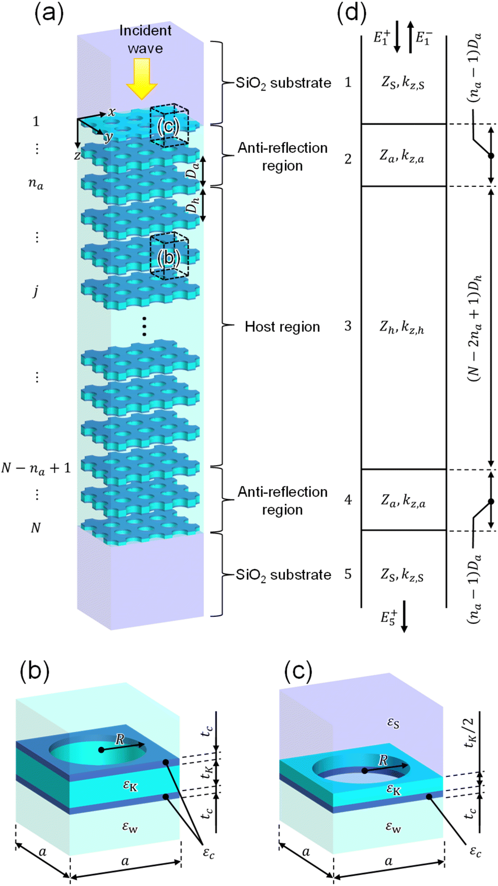
We consider a system consisting of stacked KTaO3 photonic crystal slabs with each labeled by j = 1 to N immersed in water, as shown in Fig. 2(a). The unit cell for photonic crystal slabs from j = 2 to N − 1 and the end cell j = 1 are shown in Fig. 2(b) and (c), respectively, where slab j = N is mirror-symmetric with respect to the xy plane. All of the photonic crystal slabs have square lattices with a lattice constant a = 224 nm and periodic holes with a radius of R = 0.45a [Fig. 2(b)]. They have a thickness of tK = 0.375a except for slabs j = 1 and N which have the half thickness tK/2 [Fig. 2(c)]. Thin photocatalyst layers with a thickness of tc = 0.1a are coated on both sides of each slab from j = 2 to N − 1 [Fig. 2(b)], and a photocatalyst layer is coated on one side of each of slabs j = 1 and N [Fig. 2(c)]. The regions outside of the stacked KTaO3 photonic crystal slabs consist of infinite SiO2 substrates for containing water in the structure.
 |
| | Fig. 2 (a) Configuration of a system consisting of stacked KTaO3 photonic crystal slabs in water. Each of photonic crystal slabs labeled from j = 2 to j = N − 1 has thin photocatalyst layers on both sides, and each of photonic crystal slabs labeled by j = 1 and j = N has a thin photocatalyst layer on one side. The photonic crystal slabs are regarded as the host region with the antireflection regions at both sides. (b) Unit cell of the jth photonic crystal slab (2 ≤ j ≤ N − 1). (c) End cell of photonic crystal j = 1. (Photonic crystal slab j = N is mirror-symmetric with respect to the xy plane.) Parameters are a = 224 nm, R = 0.45a, tK = 0.375a, tc = 0.1a, Dh = 1.5a, Da = 1.29a, N = 12 and na = 2. (d) Analytic model for calculating the reflection and transmission coefficients of the system of (a). Zh, Za and ZS are transverse impedances of the host and antireflection regions and SiO2 substrate, kz,h, kz,a and kz,S are wavevector components along the z-axis of the host and antireflection regions and SiO2 substrate. E+1 and E−1 are the electric fields in the 1st medium (SiO2 substrate) and E+5 is the electric field in the 5th medium (SiO2 substrate), where the superscripts + and − denote the forward and backward directions along the z axis. | |
We assume that an electromagnetic wave is illuminated on the system along the z axis at the design wavelength of λd = 400 nm (the design frequency of fd = 749.5 THz). At the interface of the SiO2 substrate and the stacked KTaO3 photonic crystal slabs, reflection would occur due to the impedance mismatch if neighboring photonic crystals have the same distance in the whole system. Here, in our system, the stacked KTaO3 photonic crystal slabs are regarded as the host region with the antireflection regions at both sides to avoid such impedance mismatch,33 where the center-to-center distances Dh = 1.5a and Da = 1.29a between neighboring photonic crystal slabs in the host and antireflection regions are slightly different. The corresponding analytic model of the system of Fig. 2(a) is shown in Fig. 2(d). It consists of the host region with the antireflection regions backed by the semi-infinite SiO2 substrates at both sides. The underlying mechanism is that the interfaces of the antireflection region with the host region and the semi-infinite SiO2 substrate are selected such that the transverse impedance has a real value, i.e., transverse impedances Zh and Za of photonic crystals in the host and antireflection regions as well as impedance ZS of the SiO2 substrates are real in Fig. 2(d). We select a number of na = 2 for the photonic crystal slabs in the antireflection region throughout the paper. The detailed discussion on the design of the antireflection region is found in ESI: Section S1.† It should be emphasized that in the system of Fig. 2, chemical reaction products around the photocatalyst layers can move through periodic holes between neighboring water regions. Therefore, our system is suitable for sunlight harvesting and artificial photosynthesis.
Theory
In this section, we present the theory for calculating absorption of the normal incident wave in the system of Fig. 2, i.e., eigenvectors and eigenvalues for the original lossless system are obtained by the revised plane wave method, which correspond to the electromagnetic fields and the wavevectors of electromagnetic modes, respectively. Using the perturbation theory with the electromagnetic fields and wavevectors above, the imaginary part of the wavevector, which represents the decay rate of the electromagnetic mode, is obtained. Using the T-matrix method with the transverse impedance, which is calculated from the electromagnetic fields, and the complex wavevector in each region, the reflection, transmission, and absorption of the system are obtained.
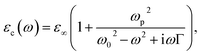
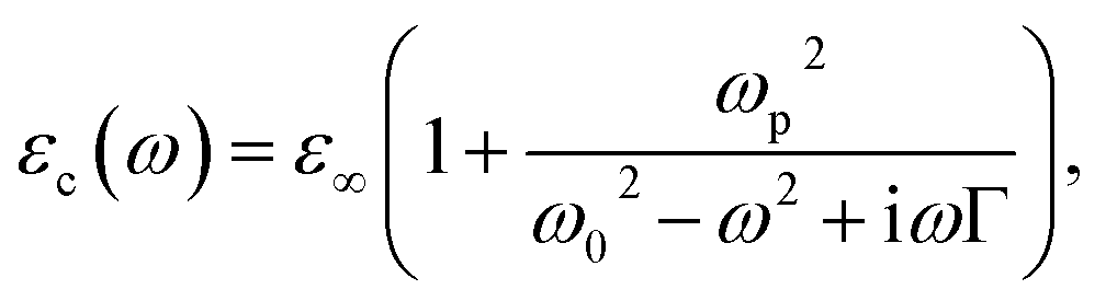
We assume that the permittivity εc(ω) of photocatalyst is given by the single-pole Lorentz model
| |
 | (1) |
where,
ω,
ωp,
ω0,
ε∞ and
Γ represent the angular frequency, the plasma frequency, the resonant frequency, the infinite permittivity, and the damping rate. We use parameters of
ωp = 1.09 × 10
16 rad s
−1,
ω0 = 7.12 × 10
15 rad s
−1,
ε∞ = 1.73 and
Γ = 7.89 × 10
14 rad s
−1 taken from the permittivity of TiO
2 in ref.
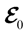
34. On the other hand, constant permittivities of
εK = 6,
εw = 1.78 and
εS = 2.1 are assumed for KTaO
3, water and SiO
2, respectively.
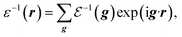
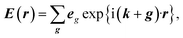
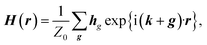
Firstly, we investigate fundamental electromagnetic properties of the infinite periodic structure of the stacked KTaO3 photonic crystal slabs corresponding the host region for the normal incidence of electromagnetic waves, i.e., the unit cell analysis. The permittivity ε(r), the electric field E(r), and the magnetic field H(r) in the first Brillouin zone are given by23
| |
 | (2) |
| |
 | (3) |
| |
 | (4) |
where
r = (
x,
y,
z) is the position vector in the coordinate system,
k = (
kx,
ky,
kz) is the wavevector,
g = (
gx,
gy,
gz) is the reciprocal lattice vector,

is the free space characteristic impedance with
ε0 and
μ0 being the free space permittivity and permeability, and

is the Fourier coefficient of the permittivity (The detailed form of the Fourier coefficient of the permittivity for the photonic crystal slab coated with photocatalyst layers is found in ESI: Section S2
†).
eg = (
ex,g,
ey,g,
ez,g) and
hg = (
hx,g,
hy,g,
hz,g) are the electric and magnetic fields, respectively. Substituting
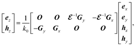
eqn (2)–(4) into Maxwell's equations, in the case of the normal incidence (
kx,
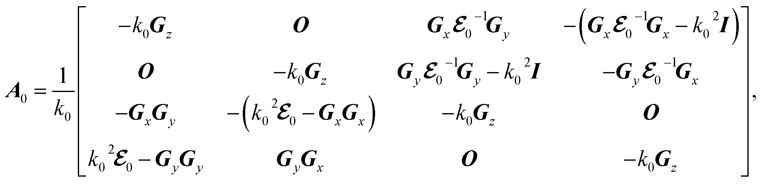
ky) = (0, 0) we consider throughout the paper, the wave equation is written as
| |
 | (5) |
where
k0 is the free space wavenumber,
Gx,
Gy, and
Gz are diagonal matrices which have diagonal components of
gx,
gy, and
gz, respectively,

is the matrix form of

,
O is the zero matrix, and
I is the identity matrix.
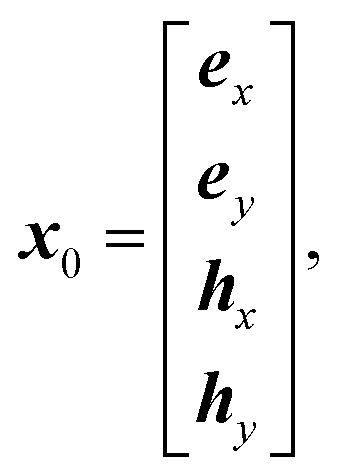
ex,
ey,
hx, and
hy are vectors with each having the
gth component of
ex,g,
ey,g,
hx,g, and
hy,g, respectively. The equation is solved for obtaining eigenvalues
kz, which allows us to treat dispersive materials in the periodic structure.
35 The
x and
y components of the electromagnetic fields are calculated from
eqn (5) as eigenvectors and the
z component is calculated from
| |
 | (6) |
where
ez and
hz are vectors with each having the
gth component of
ez,g and
hz,g, respectively. The derivations of
eqn (5) and
(6) are found in ESI: Section S3.
†
Here we use the perturbation theory.36,37 The perturbation theory allows us to treat small nonlinearities and material absorption by solving linear Hermitian eigenequations, and has been widely used to evaluate the effect of small changes in permittivities on eigenmodes and eigenvalues. The original lossless system, which is the eigenequation of eqn (5) with Γ = 0, is described by
where
kz0 is eigenvalues of the original lossless system and
| |
 | (8) |
| |
 | (9) |
where

has the matrix form of

for the lossless case. In the presence of a perturbation in the periodic structure with
A =
A0 +
A1 and

, the electromagnetic fields and the longitudinal wavevector component become
x =
x0 +
x1 and
kz =
kz0 +
kz1, respectively. Thus, we have
| | |
(A0 + A1)(x0 + x1) = (kz0 + kz1)(x0 + x1),
| (10) |
where
| |
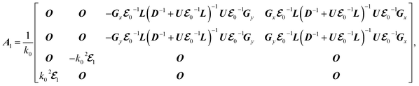 | (11) |

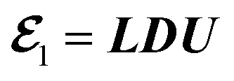
, with
L,
D, and
U being the lower triangular matrix, the diagonal matrix, and the upper triangular matrix. On the other hand, we consider left eigenvector
z0 as
For the original lossless system, we have z0 = x†0. From eqn (10) with the 1st-order terms being considered and Hermitian eigenequation of eqn (7), we have
| |
 | (13) |
Results & discussion
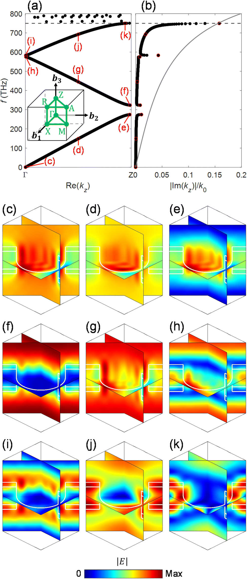
Fig. 3(a) and (b) show the dispersion diagrams of the infinite periodic structure of the photonic crystal slabs corresponding to the host region for the real and imaginary parts of the wavevector component along the z axis. The dispersion diagrams are obtained by the revised plane wave method,35 where the wave equation eqn (5) is solved at each ω for obtaining kz. The dispersion diagram is largely varied by the dimensions of the system, allowing the excitation of an appropriate electromagnetic mode at the design frequency. The dimensions a = 224 nm, R = 0.45a, tK = 0.375a, tc = 0.1a, and Dh = 1.5a in the caption of Fig. 2 have been selected so that an electromagnetic mode with the electromagnetic fields confined in the photocatalyst layers can be excited at the design frequency of fd = 749.5 THz around the top edge of the 3rd band [horizontal dashed line in Fig. 3(a)]. The imaginary part of the z component of the wavevector Im(kz), which corresponds to absorption in the thin photocatalyst layers, is significantly increased around fd = 749.5 THz [Fig. 3(b)]. This behavior can be understood from the electric field distribution of Fig. 3(k), where electric fields are confined in the two photocatalyst layers and are suppressed in the water region. It is noted that there are strong electric fields in the KTaO3 region as well in Fig. 3(k), implying that there is room for further improvement of the absorption characteristic. For other frequencies in the 3rd band, we see finite values of Im(kz) [Fig. 3(b)] since there are electric fields in the photocatalyst layers in Fig. 3(i) and (j). However, there are also electric fields in the water region in Fig. 3(i), and the water and KTaO3 regions in Fig. 3(j) as well, resulting in smaller absorption. In the 2nd band, electric fields are strong in the water region between neighboring KTaO3 substrates in Fig. 3(f)–(h), which is consistent with ref. 23. In the 1st band, electric fields are strong in the water region of the cylindrical hole in Fig. 3(c)–(e). Thus there are negligible Im(kz) for the 1st and 2nd bands. As a reference, the dispersion curve (gray solid line) of the bulk photocatalyst [eqn (1)] is plotted in Fig. 3(b). It is emphasized that Im(kz) in our system with a volume of photocatalyst less than 5%, is comparable to that of the bulk photocatalyst.
 |
| | Fig. 3 (a) Real part and (b) imaginary part of the dispersion diagram with (c)–(k) electric field distributions for the infinite periodic structure of the photonic crystal slabs corresponding to the host region, obtained by the revised plane wave method [eqn (5) and (6)] and the perturbation theory [eqn (13)]. The inset in (a) represents the 1st Brillouin zone of a photonic crystal slab with a square lattice, where Γ, X, M, Z, R and A are the points in the 1st Brillouin zone.40 b1, b2, and b3 represent reciprocal lattice vectors. The gray solid line in (b) represents the dispersion curve of the bulk photocatalyst, which is given by 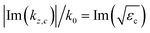 as a reference, with kz,c being the wavevector component along the z-axis in the bulk photocatalyst. as a reference, with kz,c being the wavevector component along the z-axis in the bulk photocatalyst. | |
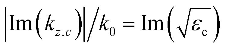
The transmission T, reflection R, and absorption A (=1 − T − R) for the system of Fig. 2 are numerically obtained by using the finite-integration based simulator CST Studio,38 and are plotted by blue lines in Fig. 4(a)–(c), respectively. We observe that near-unity absorption is achieved at the design frequency of fd = 749.5 THz [Fig. 4(c)]. The reflection R is sufficiently suppressed at the interface of the semi-infinite SiO2 substrate and the stacked KTaO3 photonic crystal structure due to the properly designed antireflection regions [Fig. 4(a)]. The transmission T is near-zero through N = 12 photonic crystal slabs due to the operation mode of Fig. 3(k) [Fig. 4(b)], where sufficient absorption occurs in the photocatalyst layers. The analytical results obtained from the analytical model of Fig. 2(d) are overlayed by the pink dotted lines in Fig. 4, which excellently agree with the numerical results (blue solid lines) for the system of Fig. 2(a) (The detailed discussion on the T-matrix method39 calculations is found in ESI: Section S4†). Discrepancy of the analytical results (pink dashed lines) from the numerical results (blue solid lines) may come from the assumption of infinite number of photonic crystal slabs (periodic structure) for obtaining transverse impedances in the host and the anti-reflection regions in the analytic model while the system of Fig. 2 has a finite number of N = 12 for the photonic crystal slabs. Fig. 4(d) shows the electric field distribution in the photonic crystal slabs at fd = 749.5 THz. We observe that the fields decay along the z axis due to absorption in the photocatalyst layers.
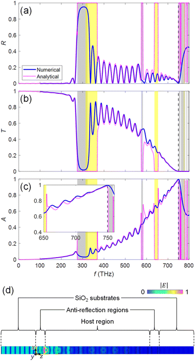 |
| | Fig. 4 Spectra of (a) reflection, (b) transmission, and (c) absorption of the system of Fig. 2. Blue solid lines and pink dotted lines represent numerical results obtained by using CST Studio and analytical results from the model of Fig. 2(d), respectively. The shaded areas with gray and yellow represent bandgaps of the photonic crystals in the host region and the antireflection region, respectively. The vertical black dashed line represents the design frequency fd = 749.5 THz. The inset in (c) represents the magnified view of absorption in the range of 650 to 750 THz. (d) Electric field distribution in the photonic crystal slabs at fd = 749.5 THz obtained by using CST Studio. | |
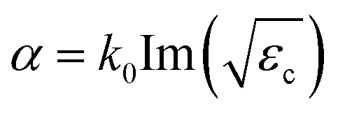
We have selected the number N = 12 of the photonic crystal slabs above for the observation of the absorption spectrum. Here, we vary the number of the photonic crystal slabs in the host region with the photonic crystal slabs in the anti-reflection region being fixed, and calculate the absorption at fd = 749.5 THz, as shown in the inset of Fig. 5(a). The numerical results (red circles) obtained using CST Studio show that the absorption of the system of Fig. 2 is higher than 80% when N ≥ 5. The absorption steeply decreases with smaller number of N due to non-zero transmission in the opposite side of the semi-infinite SiO2 substrate. For comparison, we assume an equivalent bulk medium having the same amount of photocatalyst, i.e., the medium has the thickness of tp = 2(N − 1){1 − π(R/a)2}tc. The absorption of the equivalent medium is expressed by the thickness tp and the decay rate  for the electromagnetic field as 1 − e−2αtp, and is plotted in the inset by the green line with crosses. Fig. 5(a) shows the ratio of the absorption of the system of Fig. 2 to that of the equivalent medium, which is defined as the absorption enhancement ratio. We see that the absorption enhancement ratio exceeds a factor of 3. Therefore, our results reveal that the incident light can be efficiently absorbed in small number of photonic crystal slabs, i.e., less amount of expensive photocatalyst materials. Numerical results (circles) obtained by using CST Studio agree with the analytical results (crosses with the line) obtained from the model of Fig. 2(d). Absorption spectra for various numbers N of the photonic crystal slabs are obtained in a frequency range from 650 THz to 750 THz by using CST Studio, and plotted in Fig. 5(b). With the increase of N, the absorption increases, as we expected, and is higher than 0.7 in the frequency range when N ≥ 14. The enhancement in the frequency range is clearly observed by comparing with the absorption spectra of the equivalent medium of photocatalyst in Fig. 5(c).
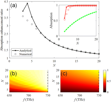 |
| | Fig. 5 (a) Absorption enhancement ratio of the system of Fig. 2 to the equivalent medium of photocatalyst with the absorption expressed as 1 − e−2αtp at fd = 749.5 THz. Black circles and the black line with crosses represent the numerical and the analytical results, respectively. The inset shows absorption of the numerical (red circles) and the analytical (red line with crosses) results of photonic crystal slabs, and the equivalent medium of photocatalyst expressed as 1 − e−2αtp (green line with crosses). (b) Absorption spectra for various numbers N of the photonic crystal slabs obtained by using CST Studio. (c) Absorption spectra of the equivalent medium of photocatalyst expressed as 1 − e−2αtp for the corresponding amount of photocatalyst. Dashed lines in (b) and (c) represent fd = 749.5 THz and their profiles are plotted in the inset of (a). Absorption spectra for various N of the photonic crystal slabs obtained from the analytic model is found in ESI: Section S5.† | |
The rate of photocatalytic reactions is generally given by RD = αϕI, with α, ϕ, and I being the absorption coefficient, the quantum yield (the ratio of the number of product molecules to the number of absorbed photons), and the intensity of the illuminated light, respectively.41 RD is proportional to αI for small I regime, and  with the increase of I. In our system, the enhancement factor of 3 corresponds to a range from
  to 3 for photocatalytic reactions. It would be interesting to develop a sophisticated model system including catalytic reactions with precious metals.
We have used the operation frequency around the top edge of the 3rd band. Above the frequency, e.g., 750.5 < ω < 800 THz, there are some modes having large Im(kz), as shown in Fig. 3(a) and (b), where |Im(kz)| > 0.2k0. However, those modes were not able to be excited by the normal incident light in the system of Fig. 2. It would be interesting to explore the excitation of those modes for higher efficiency absorption.
Conclusions
We have presented a photonic approach to enhance chemical reaction in a system consisting of stacked KTaO3 photonic crystal slabs with each having photocatalyst layers, immersed in water. Using the revised plane wave method and the perturbation theory, we have shown that electromagnetic fields are effectively confined in the photocatalyst layers at the operation in the 3rd band in the dispersion diagram. The antireflection effect was engineered by adjusting the distances between the photonic crystal slabs. As a result, an absorption enhancement of 3 was obtained compared with the bulk photocatalyst. Our photonic approach with the periodic structure, where chemical reaction products can move through holes, is a promising candidate for energy harvesting from sun and environment.
Author contributions
Taro Ikeda: conceptualization, data curation, formal analysis, investigation, methodology, software, validation, writing – original draft, writing – review & editing. Shingo Ohta: investigation, validation, writing – original draft, writing – review & editing. Hideo Iizuka: conceptualization, investigation, methodology, supervision, validation, writing – original draft, writing – review & editing.
Conflicts of interest
There are no conflicts of interest to declare.
References
- M. Aresta, A. Dibenedetto and A. Angelini, Chem. Rev., 2014, 114, 1709–1742 CrossRef CAS PubMed.
- X. Li, J. Yu, M. Jaroniec and X. Chen, Chem. Rev., 2019, 119, 3962–4179 CrossRef CAS PubMed.
- F. Li, A. Thevenon, A. Rosas-Hernández, Z. Wang, Y. Li, C. M. Gabardo, A. Ozden, C. T. Dinh, J. Li, Y. Wang, J. P. Edwards, Y. Xu, C. McCallum, L. Tao, Z.-Q. Liang, M. Luo, X. Wang, H. Li, C. P. O'Brien, C.-S. Tan, D.-H. Nam, R. Quintero-Bermudez, T.-T. Zhuang, Y. C. Li, Z. Han, R. D. Britt, D. Sinton, T. Agapie, J. C. Peters and E. H. Sargent, Nature, 2020, 577, 509–513 CrossRef CAS PubMed.
- A. Kumar, V. Hasija, A. Sudhaik, P. Raizada, Q. Van Le, P. Singh, T.-H. Pham, T. Kim, S. Ghotekar and V.-H. Nguyen, Chem. Eng. J., 2022, 430, 133031 CrossRef CAS.
- L. Wan, R. Chen, D. W. F. Cheung, L. Wu and J. Luo, J. Mater. Chem. A, 2023, 11, 12499–12520 RSC.
- H. I. Karunadasa, C. J. Chang and J. R. Long, Nature, 2010, 464, 1329–1333 CrossRef CAS PubMed.
- T. Takata, J. Jiang, Y. Sakata, M. Nakabayashi, N. Shibata, V. Nandal, K. Seki, T. Hisatomi and K. Domen, Nature, 2020, 581, 411–414 CrossRef CAS PubMed.
- P. Zhou, I. A. Navid, Y. Ma, Y. Xiao, P. Wang, Z. Ye, B. Zhou, K. Sun and Z. Mi, Nature, 2023, 613, 66–70 CrossRef CAS PubMed.
- L. Tian, Q. Xin, C. Zhao, G. Xie, M. Z. Akram, W. Wang, R. Ma, X. Jia, B. Guo and J. R. Gong, Small, 2021, 17, 2006530 CrossRef CAS PubMed.
- X. Du, L. Liu and J. Ye, Sol. RRL, 2021, 5, 2100611 CrossRef CAS.
- P. Subramanyam, B. Meena, V. Biju, H. Misawa and C. Subrahmanyam, J. Photochem. Photobiol., C, 2022, 51, 100472 CrossRef CAS.
- H. Zhou, C. Xiao, Z. Yang and Y. Du, Nanotechnology, 2020, 31, 282001 CrossRef CAS PubMed.
- L. Mascaretti and A. Naldoni, J. Appl. Phys., 2020, 128, 041101 CrossRef CAS.
- Q. Wang, C. Pornrungroj, S. Linley and E. Reisner, Nat. Energy, 2022, 7, 13–24 CrossRef.
- H. Jia, Z. Li, B. Wang, G. Xing, Y. L. Wong, H. Ren, M. Li, K.-Y. Wong, D. Lei, L.-W. Wong, J. Zhao, W. Zhang, S. Sang, A. Jian and X. Zhang, ACS Photonics, 2022, 9, 652–663 CrossRef CAS.
- C. Yang, X. Xi, Z. Yu, H. Cao, J. Li, S. Lin, Z. Ma and L. Zhao, ACS Appl. Mater. Interfaces, 2018, 10, 5492–5497 CrossRef CAS PubMed.
- X. Shi, K. Ueno, T. Oshikiri, Q. Sun, K. Sasaki and H. Misawa, Nat. Nanotechnol., 2018, 13, 953–958 CrossRef CAS PubMed.
- Z. Liu, W. Hou, P. Pavaskar, M. Aykol and S. B. Cronin, Nano Lett., 2011, 11, 1111–1116 CrossRef CAS PubMed.
- L. Yuan, J. Zhou, M. Zhang, X. Wen, J. M. P. Martirez, H. Robatjazi, L. Zhou, E. A. Carter, P. Nordlander and N. J. Halas, ACS Nano, 2022, 16, 17365–17375 CrossRef CAS PubMed.
- C. Hu, X. Chen, J. Low, Y.-W. Yang, H. Li, D. Wu, S. Chen, J. Jin, H. Li, H. Ju, C.-H. Wang, Z. Lu, R. Long, L. Song and Y. Xiong, Nat. Commun., 2023, 14, 221 CrossRef CAS PubMed.
- S. John, Phys. Rev. Lett., 1987, 58, 2486–2489 CrossRef CAS PubMed.
- J. D. Joannopoulos, P. R. Villeneuve and S. Fan, Solid State Commun., 1997, 102, 165–173 CrossRef CAS.
- J. D. Joannopoulos, S. G. Johnson, J. N. Winn and R. D. Meade, Photonic Crystals: Molding the Flow of Light, Princeton University Press, 2nd edn, 2008 Search PubMed.
- Z. Chen, L. Fang, W. Dong, F. Zheng, M. Shen and J. Wang, J. Mater. Chem. A, 2014, 2, 824–832 RSC.
- Y. Lu, H. Yu, S. Chen, X. Quan and H. Zhao, Environ. Sci. Technol., 2012, 46, 1724–1730 CrossRef CAS PubMed.
- X. Zheng, S. Meng, J. Chen, J. Wang, J. Xian, Y. Shao, X. Fu and D. Li, J. Phys. Chem. C, 2013, 117, 21263–21273 CrossRef CAS.
- Z. Cai, Z. Xiong, X. Lu and J. Teng, J. Mater. Chem. A, 2014, 2, 545–553 RSC.
- L. Sun, M. Yang, J. Huang, D. Yu, W. Hong and X. Chen, Adv. Funct. Mater., 2016, 26, 4943–4950 CrossRef CAS.
- J. Capitolis, M. Hamandi, M. Hochedel, S. El-Jallal, E. Drouard, C. Chevalier, J.-L. Leclercq, J. Penuelas, T. Dursap, S. Brottet, B. Devif, H. S. Nguyen, G. Berhault, J.-M. Chovelon, C. Ferronato, C. Guillard, E. Puzenat, N. Crespo-Monteiro, S. Reynaud, Y. Jourlin, M. Bugnet and C. Seassal, Nano Sel., 2022, 3, 108–117 CrossRef CAS.
- S. El-Jallal, M. Hochedel, J. Capitolis, H. S. Nguyen, C. Chevalier, J. L. Leclercq, M. Amara, C. Seassal and E. Drouard, Opt. Express, 2022, 30, 29694–29707 CrossRef CAS PubMed.
- M. Torras, P. Molet, L. Soler, J. Llorca, A. Roig and A. Mihi, Adv. Energy Mater., 2022, 12, 2103733 CrossRef CAS.
- Z. Wang, Y. Inoue, T. Hisatomi, R. Ishikawa, Q. Wang, T. Takata, S. Chen, N. Shibata, Y. Ikuhara and K. Domen, Nat. Catal., 2018, 1, 756–763 CrossRef CAS.
- H. Tanaka, I. Takai, H. Fujikawa and H. Iizuka, J. Lightwave Technol., 2018, 36, 2517–2523 CAS.
- E. D. Palik, Handbook of Optical Constants of Solids, Academic press, 1998 Search PubMed.
- S. Shi, C. Chen and D. W. Prather, Appl. Phys. Lett., 2005, 86, 043104 CrossRef.
- A. Raman and S. Fan, Phys. Rev. Lett., 2010, 104, 087401 CrossRef PubMed.
- A. Raman and S. Fan, Phys. Rev. B: Condens. Matter Mater. Phys., 2011, 83, 205131 CrossRef.
- Simulia, CST Studio, https://www.3ds.com/products-services/simulia/products/cst-studio-suite/, accessed July 12th, 2023 Search PubMed.
- B. E. A. Saleh and M. C. Teich, Fundamentals of Photonics, John Wiley & sons, 2nd edn, 2007 Search PubMed.
- W. Setyawan and S. Curtarolo, Comput. Mater. Sci., 2010, 49, 299–312 CrossRef.
- Y. Nosaka and A. Nosaka, Introduction to Photocatalysis: from Basic Science to Applications, The Royal Society of Chemistry, 2016 Search PubMed.
|
| This journal is © The Royal Society of Chemistry 2024 |
Click here to see how this site uses Cookies. View our privacy policy here. 
 Open Access Article
 This Open Access Article is licensed under a Creative Commons Attribution-Non Commercial 3.0 Unported Licence
 *,
Shingo Ohta
*,
Shingo Ohta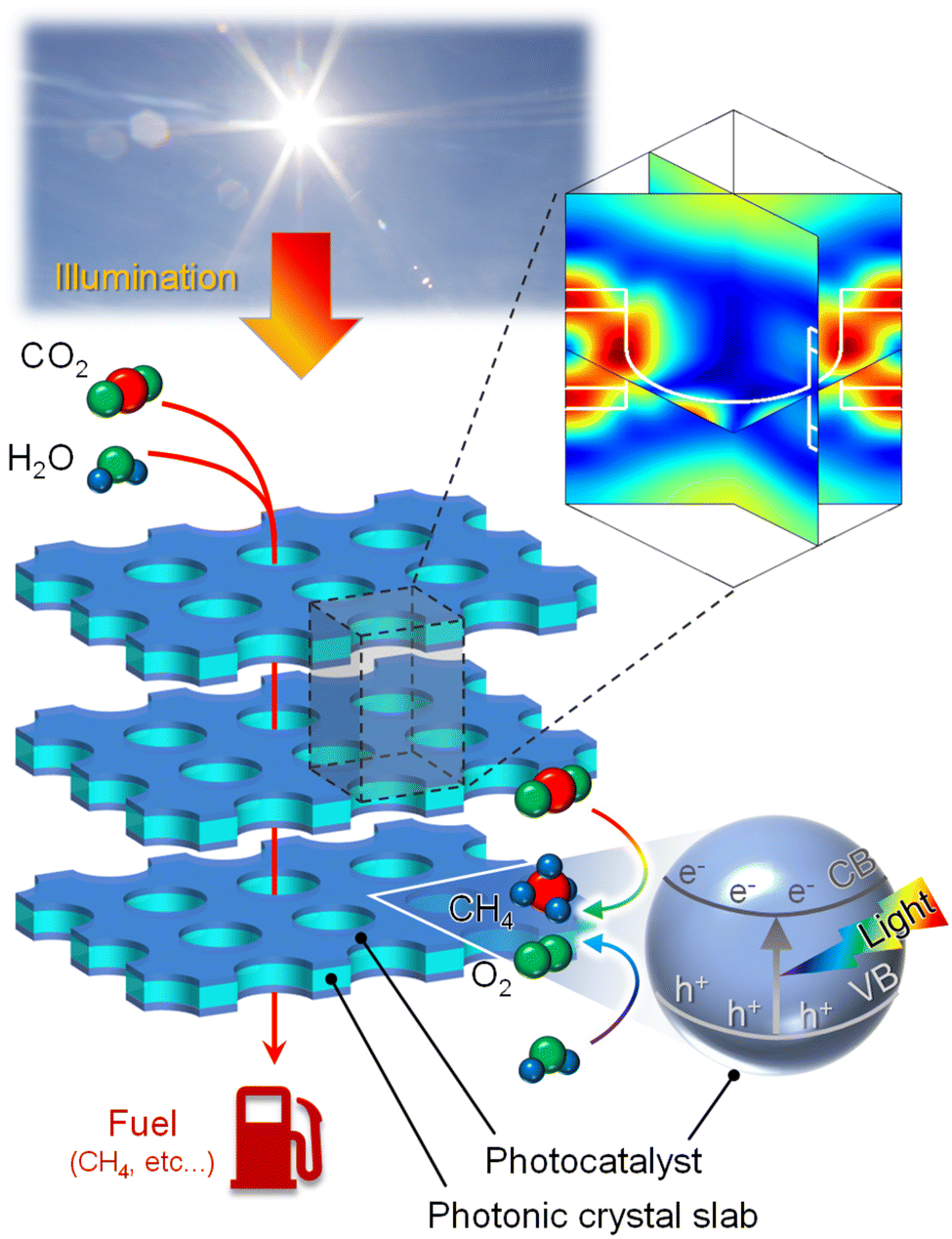
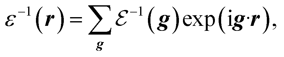


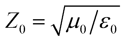 is the free space characteristic impedance with ε0 and μ0 being the free space permittivity and permeability, and
  is the Fourier coefficient of the permittivity (The detailed form of the Fourier coefficient of the permittivity for the photonic crystal slab coated with photocatalyst layers is found in ESI: Section S2†). eg = (ex,g,ey,g,ez,g) and hg = (hx,g,hy,g,hz,g) are the electric and magnetic fields, respectively. Substituting eqn (2)–(4) into Maxwell's equations, in the case of the normal incidence (kx, ky) = (0, 0) we consider throughout the paper, the wave equation is written as
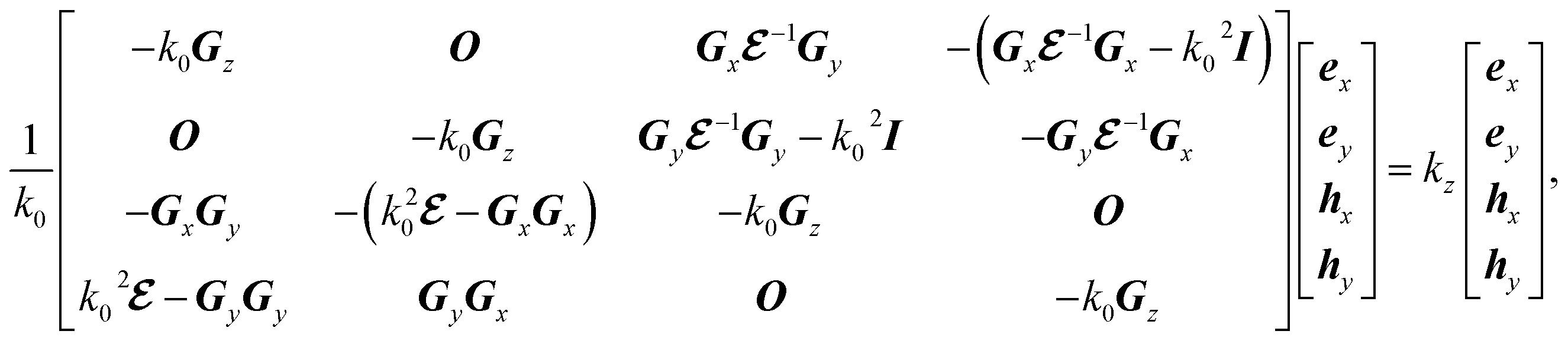
 is the matrix form of
  , O is the zero matrix, and I is the identity matrix. ex, ey, hx, and hy are vectors with each having the gth component of ex,g, ey,g, hx,g, and hy,g, respectively. The equation is solved for obtaining eigenvalues kz, which allows us to treat dispersive materials in the periodic structure.35 The x and y components of the electromagnetic fields are calculated from eqn (5) as eigenvectors and the z component is calculated from
 has the matrix form of
 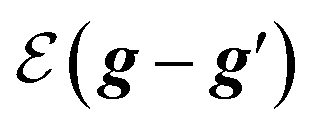 for the lossless case. In the presence of a perturbation in the periodic structure with A = A0 + A1 and
 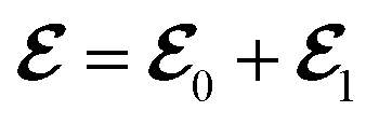 , the electromagnetic fields and the longitudinal wavevector component become x = x0 + x1 and kz = kz0 + kz1, respectively. Thus, we have
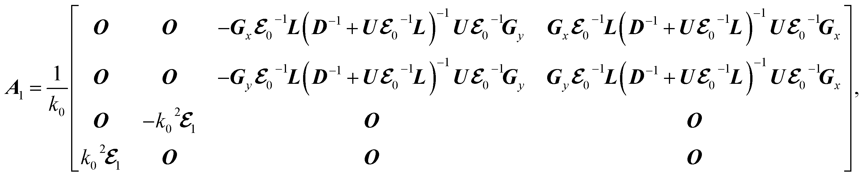
 , with L, D, and U being the lower triangular matrix, the diagonal matrix, and the upper triangular matrix. On the other hand, we consider left eigenvector z0 as
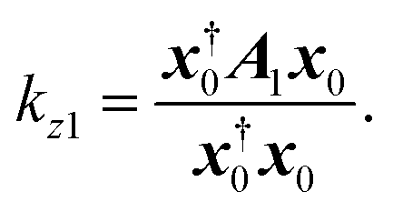
 as a reference, with kz,c being the wavevector component along the z-axis in the bulk photocatalyst.
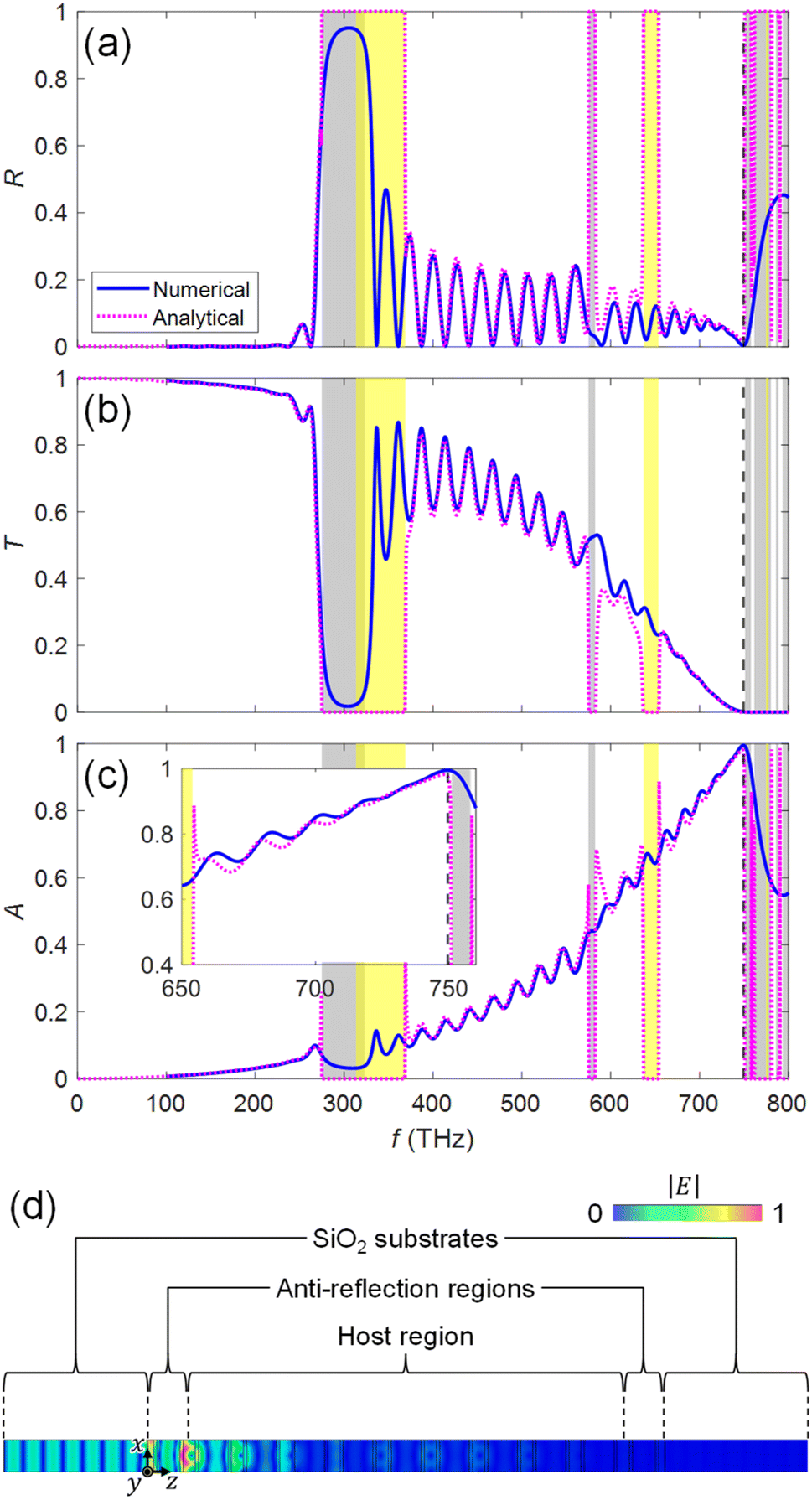
 for the electromagnetic field as 1 − e−2αtp, and is plotted in the inset by the green line with crosses. Fig. 5(a) shows the ratio of the absorption of the system of Fig. 2 to that of the equivalent medium, which is defined as the absorption enhancement ratio. We see that the absorption enhancement ratio exceeds a factor of 3. Therefore, our results reveal that the incident light can be efficiently absorbed in small number of photonic crystal slabs, i.e., less amount of expensive photocatalyst materials. Numerical results (circles) obtained by using CST Studio agree with the analytical results (crosses with the line) obtained from the model of Fig. 2(d). Absorption spectra for various numbers N of the photonic crystal slabs are obtained in a frequency range from 650 THz to 750 THz by using CST Studio, and plotted in Fig. 5(b). With the increase of N, the absorption increases, as we expected, and is higher than 0.7 in the frequency range when N ≥ 14. The enhancement in the frequency range is clearly observed by comparing with the absorption spectra of the equivalent medium of photocatalyst in Fig. 5(c).
 with the increase of I. In our system, the enhancement factor of 3 corresponds to a range from
  to 3 for photocatalytic reactions. It would be interesting to develop a sophisticated model system including catalytic reactions with precious metals.