
 Open Access Article
 This Open Access Article is licensed under a Creative Commons Attribution-Non Commercial 3.0 Unported Licence
Performance of a deep convolutional neural network to classify crystal structures using selected area electron beam diffraction patterns containing lattice defect information†
Jae Min Jeong‡
 a,
Moonsoo Ra‡b,
Jinha Jeong*b and
Woong Lee*ac
a,
Moonsoo Ra‡b,
Jinha Jeong*b and
Woong Lee*ac
aDept. of Materials Convergence and System Engineering, Changwon National University, 20 Changwondaehak-ro, Changwon-si, Gyeongsangnam-do 51140, Republic of Korea. E-mail: woonglee@changwon.ac.kr
bLightVision Inc., 20 Seongsuil-ro 12-gil, Seongdong-gu, Seoul 04793, Republic of Korea. E-mail: trizmaster@gmail.com
cSchool of Materials Science and Engineering, Changwon National University, 20 Changwondaehak-ro, Changwon-si, Gyeongsangnam-do 51140, Republic of Korea
First published on 10th June 2024
Abstract
A deep convolutional neural network (DCNN) architecture ResNet has been tested to verify its ability to handle selected area electron diffraction pattern (SADP) datasets carrying information on lattice defects including strains, thermal lattice vibrations, point defects, dislocations, and twin boundaries. The disordered states of the crystal lattices in the presence of these defects were predicted by ab initio molecular dynamics simulations, first principles geometry optimizations, and lattice manipulation operations in an effort to establish a possible dataset augmentation strategy for the improvement of classification performance of the ResNet. Using the disordered lattice information originating from the defects, test dataset SADPs were generated by simulating electron diffraction in transmission electron microscopy. The ResNet, pre-trained using SADPs from defect-free materials, showed decreasing but acceptable classification accuracies with increasing degrees of lattice disorder regarding the lattice vibrations and point defects. When tested using the diffraction patterns for strained lattices, the ResNet responded to the changing lattice symmetry when strain levels are relatively high suggesting that it has capability to discern different symmetries induced by large strains. However, the ResNet failed to recognize lattice structure when dislocations and twin boundaries were considered. It is suggested that DCNN architectures be trained over various scenarios including changes in the image feature characteristics in the diffraction patterns related to defects in future developments for improved general classification performances.
1. Introduction
The crystal structure of a material, or crystallographic symmetries specifically, has a close relation to its fundamental tensor properties such as elastic constants, electric conductivity, dielectric constants, etc1,2. Investigation of crystal structures, which is one important discipline of materials characterization, is typically carried out by analysing images including X-ray diffraction (XRD) patterns, electron backscatter diffraction (EBSD) patterns, and selected area electron diffraction (SAED or SAD) patterns.3,4 Among these, SAD patterns (SADPs) are the two-dimensional projection of the three-dimensional reciprocal lattice of a crystal structure as an outcome of the diffraction of incident electron beams at crystallographic planes of a crystalline material.5 Arrangements of diffraction spots in each SADP depend on the geometric relations between the zone axis of the specimen as aligned with the incident electron beam direction (BD) as well as on the selection rule appropriate for the given crystal system.5 Additionally, the relative intensities (brightnesses) of the diffraction spots are determined by the types and numbers of component atoms on the specific crystallographic planes of a given crystal structure.5 Interpretations of SADPs to find crystal symmetry information and lattice structure thus require in-depth knowledge of crystallography and experience with transmission electron microscopy (TEM) while the task itself is often time-consuming. It would therefore be beneficial to accelerate the materials characterization process if the analysis is performed by artificial intelligence which has demonstrated strengths in image recognition and classification using other types of diffraction patterns listed above.6–10The application of artificial intelligence, deep learning (DL) in particular, to the classification of crystal structure using SADPs is in its early development stage. Ziletti et al.11 first employed a convolutional neural network (CNN) to classify the space groups using SADP-like simulated diffraction patterns. They defined a space group descriptor by superposing diffraction patterns obtained and colour-indexed for three major crystallographic axes, namely a-, b-, and c-axes. For the selected space groups of 139, 141, 166, 194, 221, 225, 227, and 229, the training and test accuracy of 100% was reported. Tiong et al.12 constructed three colour-indexed geometric meshes by connecting diffraction spots on diffraction patterns for three major crystallographic axes as space group descriptors which were to be processed in a parallel multistream DenseNet. They achieved the classification accuracy of 80.1% over 72 space groups. The first attempt to mimic human perception process of the diffraction patterns was made in the previous work by the authors of this study.13 In this work, a CNN architecture ResNet14 was trained and validated using simulated TEM SADPs obtained for various combinations of acceleration voltages, camera lengths, and 16 zone axes ranging from [001] to [233] as appear in standard diffraction patterns. The labelling scheme based on ‘how the SADPs appear’ and the classification algorithm based on the ensemble of inference probabilities were developed and the validation accuracy of 92.6% was obtained for the space groups 213, 221, 225, 227 and 229. Further development of this scheme was reported by Chen et al. recently.15 They adopted a vector map representation of diffraction patterns obtained from the four-dimensional scanning tunnelling electron microscopy to train and validate a CNN architecture called PointNet. It was possible to identify all 7 crystal systems, from triclinic to cubic systems, instead of the space groups with the accuracy of 94%.
While these works have demonstrated application potentials of DL architectures to the analysis and classification of SADPs, there remain many issues to be addressed for further developments. For instance, the laws of thermodynamics state that no material is defect free and therefore the DL architectures should have robustness against the noisy SADPs from the specimens containing crystalline defects. Indeed, Ziletti et al. tested their CNN architecture for defects using test dataset comprising simulated diffraction patterns for materials having the vacancy concentration of up to 25% and for materials with randomly displaced lattice atoms corresponding to a few % changes in interatomic distances.11 Tiong et al. also considered the effect of vacancies by considering diffraction patterns from materials containing up to 20% of vacancy concentration as test datasets.12 These works demonstrated that their DL architectures trained and validated using datasets for defect-free or perfect crystals were robust to defect-related noisy diffraction patterns. Defects were considered from another perspective in a recent work by Chen et al. where the SADPs were artificially modified by displacing and deleting diffraction spots and adding redundant spots. It was reported that the test accuracy gradually decreased with increasing noise levels.15
Despite these attempts, it is still necessary to verify whether the DL architectures can classify noisy SADPs containing defect information further since there are more crystalline defects other than vacancies and lattice disordering. For example, thermal lattice vibration, lattice strains, impurities, dislocations, etc, can be considered.16 Noisy SADPs can be generated by adjusting positions and brightness of the diffraction spots to represent defects, while such modifications would be more realistic if performed based on actual changes in lattice structure caused by the presence of defects.17 Moreover, the previous work by the authors of this study has not been tested with noisy diffraction patterns. This previous work showed that ResNet architecture could classify space groups of materials using SADPs in its pristine form13 whereas the other works pre-processed the SADPs by colour-indexing and superpositions,11 constructing geometric meshes over them,12 or vectorizing the positions and intensities of the diffraction spots.15 From a practical viewpoint, it is desired that the crystal structure classification task be carried out using SADPs as obtained from TEM directly. In this respect, it would be necessary to test the ResNet architecture adopted in the previous study for tolerance to noises in SADPs due to crystalline defect. In this study, capability of this ResNet 101 architecture to process noisy SADPs is addressed by considering defects in single crystal systems such as lattice strains, lattice vibrations, vacancies, impurities, dislocations, and twin boundaries. Changes in the lattice structures caused by these defects were first considered using theoretical calculations, ab initio simulations and lattice simulations to generate noisy SADPs. Based on the experiment-ations using ‘realistic’ noisy SADPs, future directions for the dataset augmentation to improve crystal structure classification performance of DL architectures is discussed.
2. Dataset preparations to test the ResNet architecture for noisy SADPs
The purpose of this study is to verify the classification perform-ance of the ResNet architecture, as trained and validated to classify 5 space groups of 213, 221, 225, 227, and 229 in the previous study, regarding the noisy diffraction patterns and then to suggest future direction of the development of CNN architectures for applications to the classification of real SADPs containing defect information. The first step to these tasks is to prepare the test SADP dataset containing defect information. In the previous study, an in-house code was developed for automated generation of SADPs in large quantity by simulating electron beam diffractions in TEM.13 For the consistency of the data structure, the same code was used applying the same combinations of three acceleration voltages, three camera lengths, and 16 zone axes to generate the test SADPs.13 This code requires crystal information files (CIFs) as inputs from which virtual TEM specimens are created by repeating the unit cells 40, 30 and 20 times along three major crystallographic axes (a-, b-, and c-axes, respectively). CIFs were thus prepared to include information about defects by modifying the numbers, types, and coordinates of component atoms, and lattice parameters. Depending on the types of defects, appropriate calculations were initially carried out to find the equilibrium unit cell geometry and positions of atoms caused by defects.16,17 The calculation methods are summarized in Table 1 and detailed in the ESI.† Using the calculation results, the CIFs, initially obtained from a materials data repository Materials Project,18 were modified manually to include the changes in unit cell shapes, dimensions, and atomic positions. These CIFs were subsequently fed into the SADP generation code to obtain SADPs for materials having various types of defects (noisy SADPs). Details about the SADP generation code and the space group classification scheme can be found in the previous work.13 The ResNet architecture, trained and validated only with the SADPs from defect-free materials (clean SADPs), was then evaluated for the classification accuracies over these noisy SADPs. Since the unit cell optimization processes are computationally intensive and costly, the study has been carried out for two materials, namely Al (space group 225) and Fe (space group 229), as model systems. The overall workflow and organization of this study are shown in Fig. 1.| Type of defect | Calculation method | Output |
|---|---|---|
| Lattice strain | Solution of constitutive equation following Hook's law for anisotropic materials | Lattice parameters for deformed unit cell |
| Thermal vibration | Ab initio molecular dynamic (AIMD) simulations over 3 × 3 × 3 super cells | Disordered positions of lattice atoms |
| Point defect | First principles geometry optimizations over 2 × 2 × 2 and 3 × 3 × 3 super cells | Displaced positions of lattice atoms |
| Edge dislocation | Lattice manipulations to insert extra half planes above a slip plane | Displaced positions of lattice atoms |
| Twin boundary | Lattice manipulations to invert stacking sequences with respect to a twin plane | Mirrored positions of lattice atoms with respect to the twin plane |
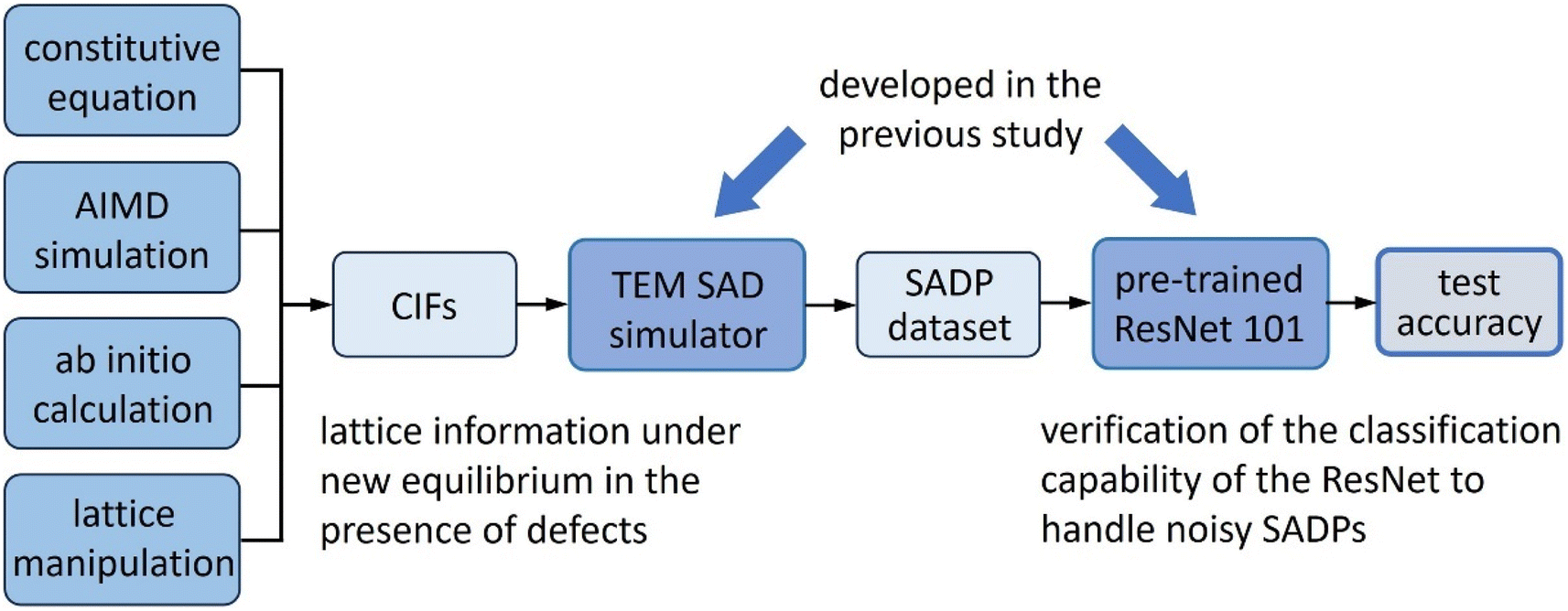 | ||
| Fig. 1 Schematic showing the data flow structure to verify the classification performance of the ResNet architecture pre-trained with SADPs for pristine defect-free materials. | ||
3. Classification accuracy of ResNet against noisy SADPs containing defect information
3.1 Uniform lattice strains
The first type of crystal defect to consider is lattice strains which cause cooperative displacements or rotation of lattice planes in specific directions. Notable examples of strains include lattice mismatch strain along the film/substrate interface.19 Fig. 2 shows how the classification accuracies of the ResNet 101 architecture change with varying strains. As for the axial strain along the a-direction, viz. [100] direction, it is seen in Fig. 2a that the strain up to about 2.5% does not have noticeable effect on the classification accuracy. Further increasing the strain in magnitude results in a rapid decrease in the classification accuracy which becomes lower than 80% when the strain is higher than 3.5%. In the case of shear strain, as seen in Fig. 2b, it does not affect the classification accuracy up to the magnitude of 0.015 rad, equivalent to the distortion of the angle γ between the a- and b-axes from 90° to 89.14°, but the accuracy decreases rapidly with further increasing strains. At the strain level of 0.03 rad (decrease in γ from 90° to 88.28°), the accuracy is lower than 70% (69.8%).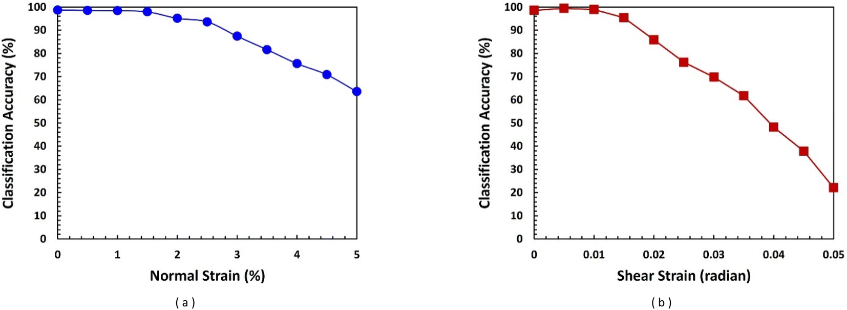 | ||
| Fig. 2 Changes in the classification accuracy of the ResNet 101 architecture with increasing magnitude of (a) the normal strain and (b) the shear strain. | ||
These changes in the test accuracy with varying strain can be understood by referring to the test SADPs for the model system of Al shown in Fig. 3 for the BD aligned with the [001] zone axis, i.e. BD = [001]. When the axial strain along a-direction, εxx, is small (2.0% in this case), the SADP in Fig. 3a is hardly distinguishable from the SADP for εxx = 0 in that the four-fold symmetry with respect to the [001] axis appear to be maintained to human eyes. Once the strain is increased (5.0% in this case), elongation between the diffraction spots is noticed along the b*-direction (vertical direction in the figure) in Fig. 3b. Concerning the shear strain, it is noticed in Fig. 3c and d that the angle between a*- and b*- directions become noticeably smaller than 90° with increasing shear strain (γxy) from 0.015 to 0.035 rad. In a strict sense, cooperative displacements, or rotations of lattice planes along specific crystallographic directions accompany changes in the lattice symmetry. However, small changes in symmetry are hardly reflected in the SADPs. Thus, human materials scientists can find proper symmetry of the material under investigation even when it is strained. Likewise, the ResNet architecture assigned proper symmetry to the strained SADPs when the strains are not large. In fact, normal strain of 1% would be reflected in the SADPs as the shift of the diffraction spot by 1 pixel in every 100 pixels while the SDAPs for the training and validation datasets had the dimension of 256 × 256 pixels. In this respect, it is expected that small magnitude of strains will not make significant change to the pixel information to be handled by the ResNet architecture.
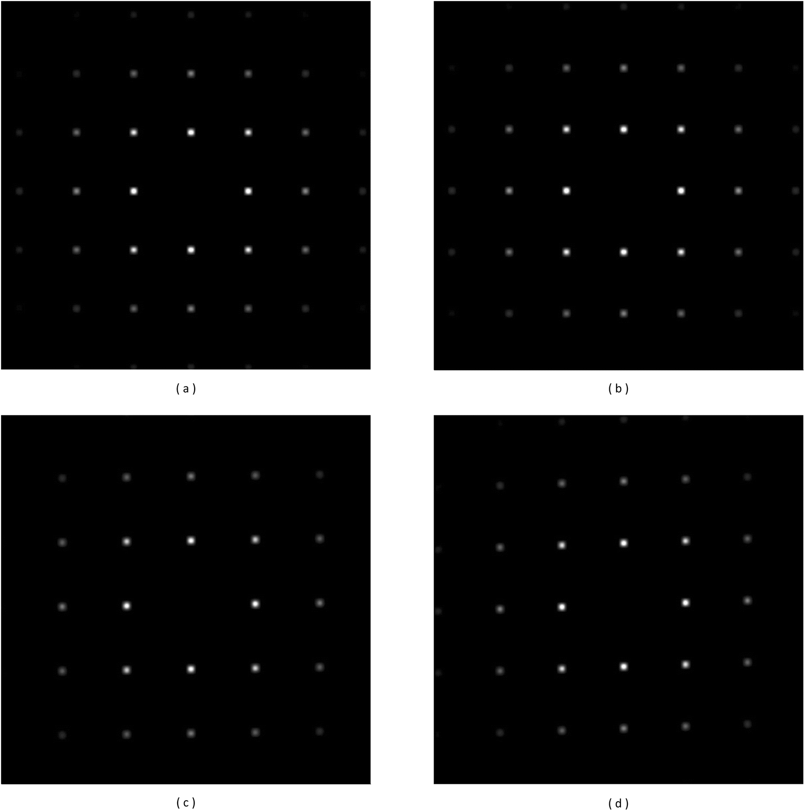 | ||
| Fig. 3 Simulated diffraction patterns for Al under uniform strains of: (a) εxx = 2.0%, (b) εxx = 5.0%, (c) γxy = 0.015 rad and (d) γxy = 0.035 rad. In the case of normal strains ((a) and (b)), distance between the nearest diffraction spots along the vertical direction (b*) is longer than that along the lateral direction (a*) in accordance with the major strain along the a-direction. In the case of shear strains ((c) and (d)), a parallelogram can be drawn by connecting four neighbouring diffraction spots as an indication of the changes in the angle between a- and b-axes due to shear strain. | ||
Decreasing accuracies at higher strains on the other hand may suggest that the ResNet 101 architecture adopted in the previous study encounter problems when treating SADPs from strained specimens. However, the ResNet 101 architecture has been trained only to classify 5 space groups in the cubic system in the previous study.13 The training datasets thus lack representations for the space groups that share similarities with the strained test SADPs. Consequently, it is expected that the ResNet architecture would try to assign the strained SADPs to one of these 5 space groups, leading to a notable decrease in classification accuracy at higher strains. Any lattices with an elongation along the a-direction is represented by the lattice parameters of a ≠ b = c and α = β = γ = 90°, which corresponds to a tetragonal system. It is therefore expected that the ResNet architecture herein would have distinguished between cubic and tetragonal symmetry, had it been trained with the diffraction dataset for the tetragonal system as well. In a similar manner, a shear strain with respect to the c-axis results in the deformed lattice with the lattice parameters of a = b = c and α = β = 90° ≠ γ, which correspond to a special case of triclinic or monoclinic system. Hence, the ResNet architecture would have assigned the SADPs for higher shear strains to monoclinic or triclinic systems like that reported by Ziletti et al.11
3.2 Thermal lattice vibrations
Strain in a lattice structure is a systematic and collaborated shift of atomic positions. Therefore, any basic repeating unit (unit cell) in a strained lattice can be perfectly matched to other unit cells by translational transforms. In comparison, thermal vibration causes random motions of the lattice atoms which shift off the sites of perfect periodic lattice. Unless the system temperature is 0 K, lattice atoms always have thermal energy, and the resulting thermal vibrations of lattice atoms cause their dynamic and random displacements in random directions.16 The instantaneous positions of Al atoms in the 3 × 3 × 3 supercell were predicted to be displaced randomly as shown in Fig. 4a and b for 100 K and 300 K, respectively by the AIMD simulations described in the ESI S2.† The distribution of the displacements in atomic positions along the x-direction (displacement distribution in the other two directions were similar) are also shown in Fig. 4c and d, in which it is seen that disordering by thermal energy is more pronounced at 300 K compared to that at 100 K. While the largest displacement of the atomic position at 100 K was 0.086 Å, 85 out of 108 atoms in the supercell had displacements smaller than 0.04 Å (about 1% of the unit cell length of 4.05 Å). At 300 K, the largest displacement increased to 0.15 Å and 88 out of 108 atoms showed displacements smaller than 0.08 Å (about 2% of the unit cell length). In TEM, electrons in the beams travel at speeds in the order of 108 m s−1, while the lattice vibration frequency is in the order of 1012 s−1. Hence, an SADP from a TEM specimen, typically much smaller than 100 nm in thickness, will be the result of an average over the different ‘instantaneous’ positions of the thermally displaced lattice atoms and consequently consists of diffuse diffraction spots with decreased intensities.5,20 This is also visible in the simulated SADPs shown in Fig. 5, obtained from Al virtual specimen at the temperatures of 0, 100, 300 K, respectively, which were generated from the CIFs containing the atomic positions affected by thermal disorder except the case of 0 K, for BD = [001]. It is seen that the brightnesses (intensities) of the diffraction spots especially for the higher index planes (those located around the inner brighter spots) decreases slightly with increasing temperatures.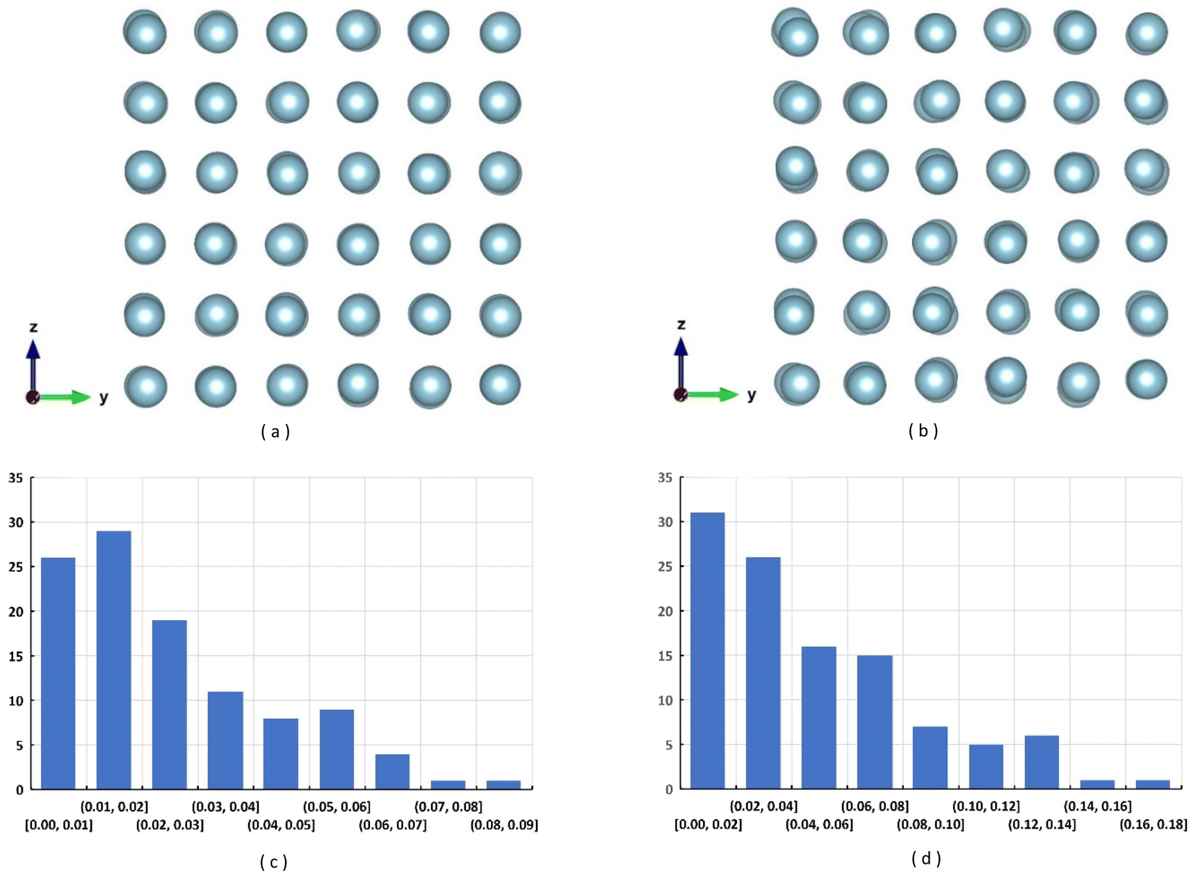 | ||
| Fig. 4 Instantaneous positions of Al atoms due to thermal lattice vibrations in the 3 × 3 × 3 supercell predicted by the AIMD simulation at (a) 100 K and (b) 300 K and histograms showing the corresponding distribution of the displacements in atomic positions along the x-direction at (c) 100 K and (d) 300 K. | ||
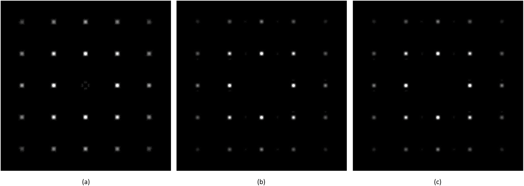 | ||
| Fig. 5 Simulated SADPs from an Al virtual specimen at the temperature of (a) 0 K, (b) 100 K, and (c) 300 K using the CIFs containing the disordered positions of the lattice atoms due to thermal vibrations. | ||
Although lattice structures were predicted to be disordered due to thermal vibrations causing diffuse scattering of the electron beams as revealed in the resulting simulated SADPs, the classification capability of the ResNet architecture was not significantly influenced by the changes in the intensities of the diffraction signals. It exhibited the classification accuracy of 94.57 and 90.13% for the Al superlattices with simulated thermal disordering at 100 and 300 K, respectively. These accuracies are not much different from that for the diffraction patterns obtained at 0 K which was 98.65% demonstrating the robustness of the ResNet architecture in classifying the diffraction data having thermal noises originating from disordering. Gradual decrease in the accuracy with increasing temperature is the result of an increasing degree of disorder16 which resulted in more noises in the diffraction signals.
If lattice atoms are randomly displaced in direction, the crystal structure will have P1 symmetry (space group 1). However, such random displacements can be averaged over many atoms. Further, these displacements are only very small fractions of lattice lengths as mentioned above and shown in Fig. 4c and d. Hence, random changes in the atomic positions due to thermal vibration will not affect the lattice symmetry reflected in the SADPs. They only cause small changes in the intensities (brightness) of the diffraction spots5,20 that could be handled by the ResNet architecture without significant loss of accuracies. This is similar to the human perception process in which the geometric arrays of the diffraction spots are first recognized to assign the SADP of concern to an appropriate space group and then the diffuse diffraction spots are ascribed to the presence of some defects.5,20,21
3.3 Point defects
Another cause of deviation from the perfect ordering of lattice structures is the presence of point defects such as vacancies and impurities. Vacancies exist in materials unless the temperature of the system is 0 K while no material is free of impurities in accordance with the laws of thermodynamics of solutions.17 Existence of a point defect at a lattice site to empty (like a vacancy) or occupy (like substitutional impurity) it changes the energy state in its vicinity. New equilibrium is then established by displacing the neighbouring atoms from their original lattice points.20,21 Such displacements are larger near a defect than away from it, which results in a local strain field. If the defect concentration is high, these local strain fields would overlap leading to global lattice deformations. In a material at equilibrium, one vacancy occurs in about every 1015 atoms at room temperature,22 too small to have any effect on the electron diffraction process in TEM. Meanwhile, there are solubility limits of impurities (solutes) and many practical alloy systems contain them in the range of only a few %. Alloys with high impurity (solute) concentrations often assume new lattice structures (new phases), another equilibrium state.17The classification capability of the ResNet architecture with respect to the point defects was verified with rather high defect concentrations of 1/32 (3.1 at%, 2 × 2 × 2 supercell) and 1/108 (0.93 at%, 3 × 3 × 3 supercell) for Al and 1/54 (1.8 at%, 3 × 3 × 3 supercell) and 1/128 (0.78 at%, 4 × 4 × 4 supercell) for Fe, respectively. Lattice deformations caused by the point defects of these concentrations, as predicted from the first principles geometry optimization, are visualized as projections of lattice points onto the x–y plane (viewing direction is [001]) in Fig. 6. It is seen that the lattice distortions are higher for higher defect concentrations while the vacancy tends to deform lattices more than substitutional impurities, which are more pronounced in Fe than in Al lattices. For instance, in 2 × 2 × 2 Al superlattice, among 31 lattice atoms, 8 atoms around a vacancy showed the largest displacement of the atomic position of 0.036 Å in the first principles geometry optimization while the remaining 23 atoms showed almost zero displacements. In 3 × 3 × 3 Fe superlattice, among 53 lattice atoms, 10 atoms around the vacancy were displaced by 0.14 Å, 26 atoms in the surrounding regions were displaced by 0.045 to 0.12 Å and the remaining 17 atoms showed almost zero displacements. In these deformed superlattices, locations of the defects were chosen arbitrarily, but these deformed lattices are repeated along the x, y, and z directions 10 times to create virtual specimens resembling nanoparticles to generate SADPs in the TEM SAD simulations. Hence, in these virtual TEM specimens, the defects themselves form another ordered array affecting the diffraction process, which would provide severer conditions with respect to causing ‘noises’ in the SADPs than defects with completely random distributions.
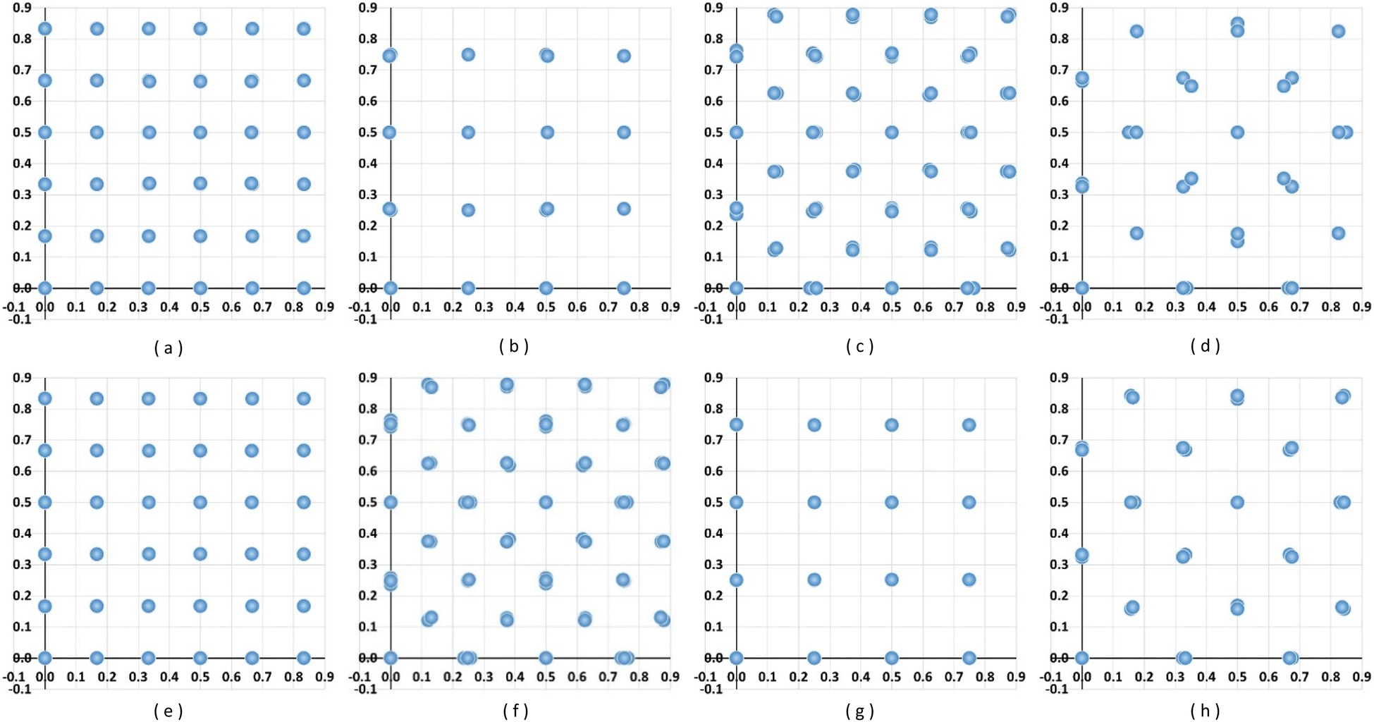 | ||
| Fig. 6 Disordered positions of lattice atoms due to the presence of: a vacancy in (a) Al 3 × 3 × 3 supercell, (b) Fe 4 × 4 × 4 supercell, (c) Al 2 × 2 × 2 supercell, and (d) Fe 3 × 3 × 3 supercell; or a substitutional impurity in (e) Al 3 × 3 × 3 supercell, (f) Fe 4 × 4 × 4 supercell, (g) Al 2 × 2 × 2 supercell and (h) Fe 3 × 3 × 3 supercell. | ||
Fig. 7 shows the simulated SADPs from Fe with point defects for [001] zone axis. In these diffraction patterns the relative intensities of the diffraction spots for higher index planes (smaller dots around the inner brighter ones) becomes weaker with the introduction of defects to the lattice, which is more prominent for the case of vacancy. Such changes in the diffraction patterns subsequently result in the changes in the classification accuracy as summarized in Table 2 regarding the vacancies and substitutional impurities. As expected, presence of point defects in materials at low concentrations do not have noticeable effect on the classification accuracy. Once the defect concentrations increase, the accuracy becomes lower. Especial-ly when the defect type is vacancy which caused large lattice distortion in substantial volume of the Fe supercell (Fig. 6d), decrease in the accuracy is somewhat noticeable, although 83.24% seems to be still acceptable. This indicates that large non-uniform deformation in lattice structure and resulting diffuse scattering of electrons as reflected in the degraded quality of the SADPs has detrimental effect on the classification accuracy, although it is still acceptable when the defect concentration within practical ranges.
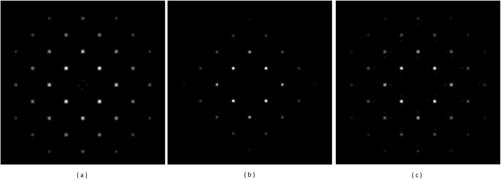 | ||
| Fig. 7 SADPs obtained from (a) pristine Fe lattice, (b) Fe 3 × 3 × 3 supercell with one vacancy and (c) Fe 3 × 3 × 3 supercell with one Au atom substituting one lattice Fe atom. | ||
| Type of defect | Defect concentration in supercells | Classification accuracy |
|---|---|---|
| Vacancy | Al 3 × 3 × 3 supercell: 1/108 | 97.79% |
| Fe 4 × 4 × 4 supercell: 1/128 | ||
| Al 2 × 2 × 2 supercell: 1/32 | 83.24% | |
| Fe 3 × 3 × 3 supercell: 1/54 | ||
| Substitutional impurity (si in Al/Au in Fe) | Al 3 × 3 × 3 supercell: 1/108 | 97.55% |
| Fe 4 × 4 × 4 supercell: 1/128 | ||
| Al 2 × 2 × 2 supercell: 1/32 | 94.90% | |
| Fe 3 × 3 × 3 supercell: 1/54 |
In some materials systems, foreign atoms smaller than the hosting lattice atoms may occupy the interstitial sites. Since the interstitial sites do not provide enough volume to accommodate the impurity atom, neighbouring lattice near the impurity is distorted. Depending on the size of the impurity, the extent of distortions may differ. In the case of C impurity taking a tetrahedral site in Al lattice, the first principles geometry optimization for a 3 × 3 × 3 supercell (one C atom in 108 Al atoms) predicted that the lattice distortion is limited only to the first neighbouring lattices as shown in Fig. 8a. This highly localized lattice deformation did not have a noticeable effect on the diffraction process when the SADP in Fig. 8b is compared with that for a defect-free Al in Fig. 5a. The classification accuracy for the SADPs for this system was 95.48%, close to the accuracy of 98.65% for the SADPs from a pristine Al single crystal.
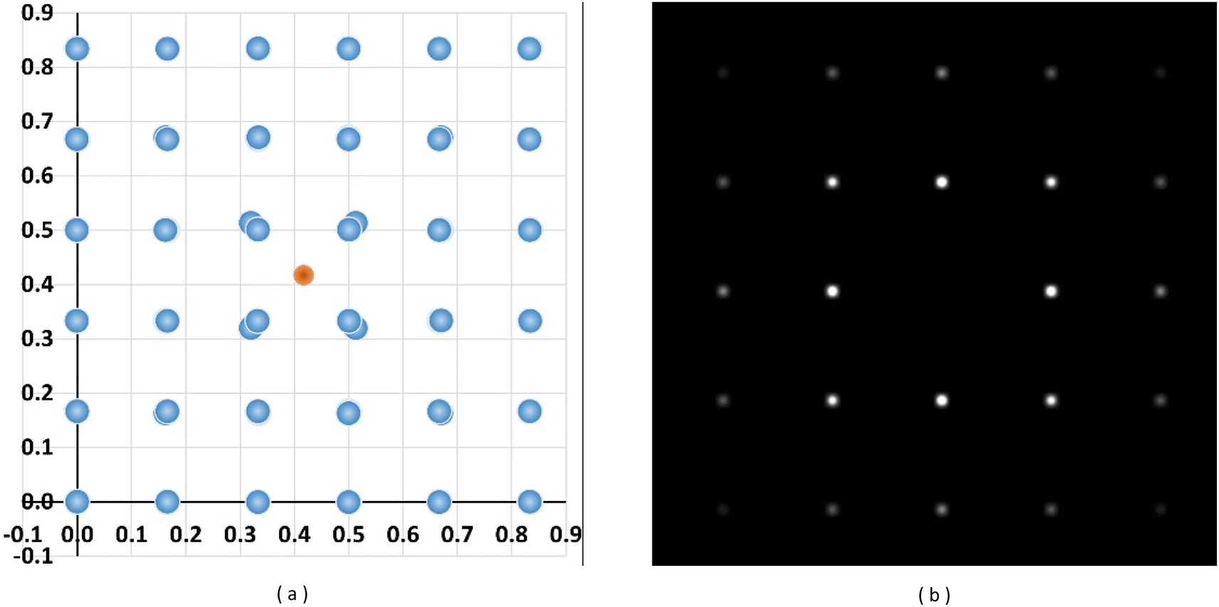 | ||
| Fig. 8 (a) Predicted atomic positions when a C atom occupies a tetrahedral interstitial site in an Al 3 × 3 × 3 supercell and (b) corresponding simulated SADP for BD = [001]. | ||
3.4 Dislocation and twin boundary
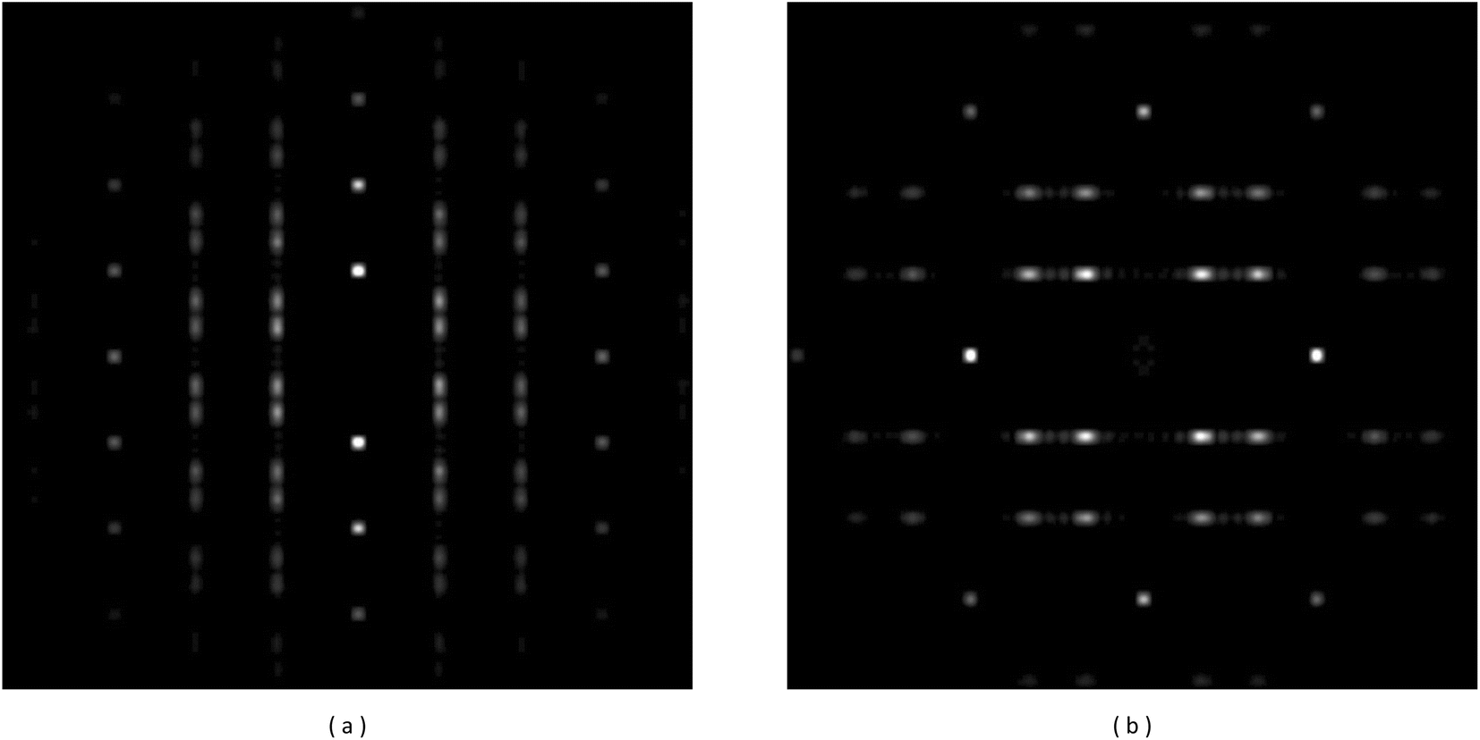
Considerations of lattice defects so far suggest that the ResNet 101 architecture, as trained and validated with simulated SADPs for defect-free materials in the previous study, retains its classification accuracy within acceptable range while it deteriorates with increasing degree of lattice disordering attributable to defects. However, this is not the case for the defects of higher dimensions such as edge dislocations (linear defects) and twin boundaries (planar defects). Edge dislocation is introduced when an extra half plane exists normal to a slip plane resulting in mismatched arrangements of lattice atoms along the slip plane. Consequently, the lattice around a dislocation core is distorted.23 In some cases, edge dislocations may form a periodic array to have a long-range ordering. In simulating the electron diffraction process through a virtual Al single crystal specimen in this study, an array of four edge dislocation with the line vector of [112] and the Burgers vector of [110]/2 was considered,23 and the resulting SADPs are shown in Fig. 8a–c for the [112], [111], and [110] zone axes, respectively. The array of diffuse disk-like diffraction spots with some streaks in Fig. 9a and double spots in Fig. 9b are the footprints of the dislocation array and associated lattice strains.22 Additional features found in this simulated SADP are a rotational symmetry of order 2 in Fig. 9a and mirror symmetry in Fig. 9b, which is attributed to the presence of an extra half plane.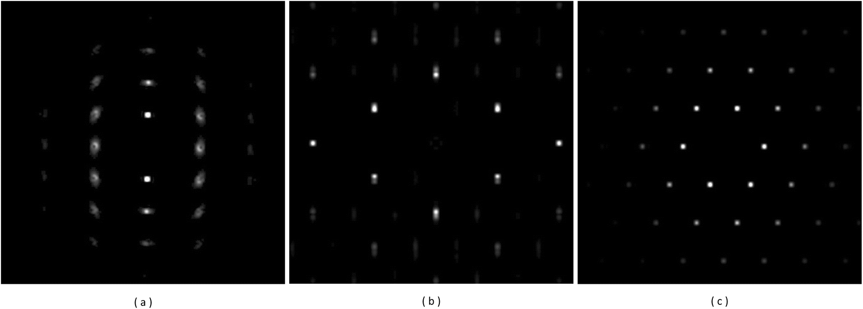 | ||
| Fig. 9 SADP from Al having an array of fours edge dislocations having the Burgers vector of [110]/2. The virtual specimen was aligned with (a) BD = [112], (b) BD = [111] and (c) BD = [110], respectively. | ||
Unlike the cases of lattice strain, thermal vibration, and point defects, the ResNet architecture failed to classify these SADPs showing the classification accuracy only of 7.97%. The image features included in the SADPs from specimens containing dislocations are diffuse disks with streaks. These features are obviously different from diffraction spots included in the SADPs for training the ResNet, viz. SADPs from defect-free specimens.13 A human materials scientist will resort to knowledge and experiences to assign the SADPs in Fig. 9 to the space group 225 for the zone axes of [112], [111], and [110], respectively from the overall arrangements of the diffraction spots. Those specific features such as diffuse disks and streaks will then be ascribed to the dislocation array.22 On the other hand, the ResNet architecture tries to match the image to the closest model (function) that has been established during the training process. If the features in the test image are substantially different from those in the training image dataset such that the ‘noises’ are essentially new features, then the ResNet will fail to classify the image properly.
Failure of the ResNet in classifying SADPs is further expected when a TEM specimen contains a twin boundary which forms a mirror plane between two crystals having the same crystal structure but inverted stacking sequences. Hence, the SADPs from a specimen having a twin boundary will appear as a superposition of two diffraction patterns reflected with respect to each other if the beam direction is normal to both the twinning direction and twinning plane normal. SADPs from specimens containing one twin boundary are shown Fig. 10a and b for the model systems of Al and Fe, respectively. In Al, the twin plane is (111) and the twinning direction is [112]24 and Fig. 10a was obtained for BD = [110]. As for Fe, the twin plane is (121) and the twinning direction is [111]20 and Fig. 10b was obtained for BD = [101]. These SADPs differ substantially from the standard diffraction patterns as exemplified by the double or quadruple diffraction spots with large separations which are the traces of twins. For the SADPs from the twinned crystals, the ResNet architecture showed the classification accuracy of 33.80%. In the case of SADPs from materials with twin boundaries, difficulty arises even to a human materials scientist unless the overlapping of two inverted patterns is noticed by analysis or intuition based on experiences. Since an SADP from a material containing twin boundary is essentially a superposition of two reflected SADPs, it can be treated as an SADP of different kind containing new features like SADPs from textured structures. In the latter case, several essentially identical SADPS are superposed with small rotations around an axis normal to the centre of the incident electron beam. Such a feature was not included in the training dataset,13 and therefore the SADPs from a twin system would be treated as unknown type rather than noisy patterns. It would then be natural to expect that the ResNet is unable to classify an SADP like the case of dislocations.
 | ||
| Fig. 10 Simulated diffraction patterns for (a) Al (BD = [110]) and (b) Fe (BD = [101]) single crystals with one twin boundary. | ||
3.5 Remarks on the classification of crystal structures using noisy SADPs due to lattice defects
In machine learning and deep learning, a classification task involves defining regions in a multi-dimensional feature space, where each region is associated with a specific label. This ensures that every input, such as SADPs, falls within one of the predefined categories (labels). Consequently, there are no undefined regions, and all data points are assigned to one of the five space groups for which the ResNet architecture has been trained and validated with clean SADPs from defect-free virtual specimens. This scenario, known as a closed-set problem, characterizes the proposed ResNet SADP analysis system.25 While inferring a space group from SADPs is itself a closed-set problem with a potential of expansion to all 230 space groups, the classification system used at this stage is limited to analysing only five specific space groups. Inevitably, the system must confront the challenge of dealing with unknown labels when noisy SADPs containing defect information, especially regarding lattice strains, dislocations, and twin boundaries, are input for the classification. How to effectively handle such unfamiliar data remains an ongoing area of investigation. Incorrect label inferences may result from improperly shaped decision boundaries generated by the trained deep learning model. Throughout the training phase, the model aims to minimize a loss function, prioritizing high classification accuracy.26 As a result, the fine-tuning of decision boundaries is not directly within the control of the human user. Instead, adjustments are made indirectly through modifications to the training data and loss function for example.27,28 Consequently, system failures may not align perfectly with human perception. Therefore, the development of a suitable loss function tailored for analysing SADP will be another subject for future research.Considering the theoretical foundations of deep learning, the ResNet architecture's robustness against defects demonstrated in this study, be it strong as in the case of lattice disorder and point defects or weak as in the case of dislocations and twin boundaries, may hinge on two key factors. One is the dimensions of the SADPs utilized during training and the other is composition of the dataset, which includes the data augmentation technique.29,30 Concerning the dataset dimension, it was found in a preliminary investigation that the ResNet became more sensitive to even smaller defect-related noises in the dataset if the simulated SADPs for training have resolution exceeding 256 × 256 pixels. This susceptibility arises from the detailed changes present in the simulated SADPs due to the defects themselves. On the contrary, decreasing the image resolution would result in the loss of details in the lattice structure information, leading to degradation of general classification capability even over the pristine (clean) SADPs.
Meanwhile, most of the limitations in the ResNet architectures performance encountered in this study stem from the dataset characteristics. Despite the exceptional performances of recent deep learning applications, their success often depends on vast quantity training data that comprehensively covers various real-world scenarios. On the other hand, tasks such as SADP classification pose challenges in acquiring datasets that encompass nearly all real-world cases, an almost impossible work. Therefore, employing appropriate data augmentation techniques and/or more comprehensive SADP simulations becomes crucial in overcoming such limitations. As demonstrated in this study as well as in the previous studies elsewhere,11,12 the DL architectures are robust against noisy SADPs originating from low dimensional defects since the ‘noises’ in this case are small changes in the brightness of the diffraction spots. On the other hand, as seen in this study, defects of higher dimensions introduce new features in the SADPs that are not included in the ‘clean’ training SADP datasets, which leads to substantial decrease in the classification accuracies. Hence, one possible strategy of dataset augmentation for improved classification accuracy over the noisy SADPs would be the preparation of training and validation datasets having these new features due to dislocations and twin boundaries. At this stage, however, it is a challenging task to prepare noisy SADPs for these defects for numerous materials systems in large quantity. One possible alternative method to tackle this problem would be the use of image translation strategies such as cycle-GAN31 by which the test SADPs containing high dimensional defect information can be transformed into those resembling the ‘clean’ training dataset. Considering these factors for enhancing the performance of deep learning models would stand as a key direction for future developments.
4. Conclusions
From the results for the classification accuracies regarding the defects in this study, a general trend in the classification capability of the ResNet architecture for the SADPs containing defect information can be summarized as follows. A uniform lattice deformation incurs cooperative displacements of lattice plane and will accompany changes in lattice symmetries. It is therefore natural for ResNet architectures to assign the strained SADP to other space groups corresponding to new symmetries. However, the ResNet architecture adopted in this study has some tolerance to lattice deformation such that it classifies the SADP to the space group of original symmetry if the strain was low in magnitude, like human materials scientists. If the lattice distortion is random as in the case of thermal vibration, there would be many variations in the distortions of lattice structures. Such ‘disordering’ was revealed as small changes in the SADPs, but the ResNet architecture could classify these patterns properly with slight decreases in the accuracies demonstrating some tolerance to the noises in the SADPs. Pertaining to the point defects, the performance of the ResNet architecture depended on the extent of the lattice distortion due to the defects. If the distortion is small and/or localized to the vicinity of the defect, the classification accuracy did not suffer much, but it deteriorated substantially, although still acceptable, once the lattice deformation was large or extended over long ranges. However, the ResNet failed to recognize the SADPs from materials containing edge dislocations and twin boundaries, since the pattern included ‘new’ features that could not be handled within the ‘knowledge’ of the ResNet due to lack of training. The results in this study place a question on the dataset preparation for training DCNN architecture in general. One possible direction would be to include all possible cases revealed in the image features due to defects as well as equipment conditions in real microscopy by extensive and comprehensive diffraction simulations and dataset augmentations, which is another challenge to the application of computer vision to materials characterizations.Author contributions
The manuscript was structured and written jointly by all authors. Each author shared expertise and knowledge as well as insight on the results. Jae Min Jeong (JMM) prepared the CIFs containing defect information after carrying out the necessary calculations including AIMD simulations and first principles geometry optimizations. This is followed by SADP generation through simulations and the series of tests to verify the performance of the ResNet regarding noisy patterns. Moonsoo Ra (MR) was responsible for developing the diffraction simulation code, developing the ResNet architecture specific to diffraction pattern classification, and the training and validation of the ResNet. Jinha Jeong (JJ), as the primary investigator (PI) of this research, organized and supervised all the research, reviewed the results, and commented on the contents of this manuscript. Woong Lee (WL), the co-PI, organized and supervised this research, designed the process to generate CIFs containing the lattice defect information, planned the AIMD and first principles calculations as well as the diffraction simulation. This was followed by the interpretation of all the data and feedback on further research work if necessary.Conflicts of interest
There are no conflicts to declare.Acknowledgements
This work was supported by Institute of Information & communications Technology Planning & Evaluation (IITP) grant funded by the Korea government (MSIT) (2020-0-000302, Development of AI based Material Crystal Structure Analysis Solution and Service).Notes and references
- R. E. Newnham, Properties of Materials: Anisotropy, Symmetry, Structure, Oxford University Press, New York, 2005 Search PubMed.
- U. Müller, Symmetry Relations between Crystal Structures, Oxford University Press, Oxford, 2013 Search PubMed.
- B. D. Cullity and S. R. Stock, Elements of X-Ray Diffraction, Pearson Education Limited, Harlow, 3rd edn, 2014 Search PubMed.
- L. Reimer and H. Kohl, Transmission Electron Microscopy, Springer, New York, 5th edn, 2008 Search PubMed.
- D. B. Williams and C. B. Carter, Transmission Electron Microscopy: A Textbook for Materials Science, Springer, New York, 2009 Search PubMed.
- W. B. Park, J. Chung, J. Jung, K. Sohn, S. P. Singh, M. Pyo, N. Shin and K.-S. Sohn, IUCrJ, 2017, 4, 486–494 CrossRef CAS PubMed.
- F. Oviedo, Z. Ren, S. Sun, C. Settens, Z. Liu, N. T. P. Hartono, S. Ramasamy, B. L. DeCost, S. I. P. Tian, G. Romano, A. G. Kusne and T. Buonassisi, npj Comput. Mater., 2019, 5, 60 CrossRef.
- P. M. Vecsei, K. Choo, J. Chang and T. Neupert, Phys. Rev. B, 2019, 99, 245120 CrossRef CAS.
- J. A. Aguiar, M. L. Gong, R. R. Unocic, T. Tasdizen and B. D. Miller, Sci. Adv., 2019, 5, eaaw1949 CrossRef CAS PubMed.
- K. Kaufmann, C. Zhu, A. S. Rosengarten, D. Maryanovsky, T. J. Harrington, E. Marin and K. S. Vecchio, Science, 2020, 367, 564–568 CrossRef CAS PubMed.
- A. Ziletti, D. Kumar, M. Scheffler and L. M. Ghiringhelli, Nat. Commun., 2018, 9, 2775 CrossRef PubMed.
- L. C. O. Tiong, J. Kim, S. S. Han and D. Kim, npj Comput. Mater., 2020, 6, 196 CrossRef.
- M. Ra, Y. Boo, J. M. Jeong, J. Batts-Etseg, J. Jeong and W. Lee, RSC Adv., 2021, 11, 38307–38315 RSC.
- K. He, X. Zhang, S. Ren and J. Sun, IEEE Conference on Computer Vision and Pattern Recognition (CVPR), Las Vegas, NV, 2016, pp. 770–778 Search PubMed.
- J. Chen, H. Zhang, C. B. Wahl, W. Liu, C. A. Mirkin, V. P. Dravid, D. W. Apley and W. Chen, Proc. Natl. Acad. Sci. U. S. A., 2023, 120, e2309240120 CrossRef CAS PubMed.
- S. O. Kasap, Principles of Electronic Materials and Devices, McGraw-Hill, New York, 4th edn, 2018 Search PubMed.
- D. A. Porter, K. E. Easterling and M. Y. Sherif, Phase Transformations in Metals and Alloys, CRC Press, Boca Raton, 4th edn, 2021 Search PubMed.
- A. Jain, S. P. Ong, G. Hautier, W. Chen, W. D. Richards, S. Dacek, S. Cholia, D. Gunter, D. Skinner, G. Ceder and K. A. Persson, APL Mater., 2013, 1, 011002 CrossRef.
- P. A. Gabrys, S. E. Seo, M. X. Wang, E. Oh, R. J. Macfarlane and C. A. Mirkin, Nano Lett., 2018, 18, 579–585 CrossRef CAS PubMed.
- B. Fultz and J. Howe, Transmission Electron Microscopy and Diffractometry of Materials, Springer Berlin, Heidelberg, 4th edn, 2012 Search PubMed.
- C. B. Carter and D. B. Williams, Transmission Electron Microscopy: Diffraction, Imaging, and Spectrometry, Springer, Cham, 2016 Search PubMed.
- W. D. Callister and D. G. Rethwisch, Materials Science and Engineering: an Introduction, Wiley, Hoboken, 9th edn, 2015 Search PubMed.
- D. Hull and D. J. Bacon, Introduction to Dislocations, Butterworth-Heinemann, Oxford, 2011 Search PubMed.
- J. D. Verhoeven, Fundamentals of Physical Metallurgy, John Wiley and Sons, New York, 1975 Search PubMed.
- Y. Wen, K. Zhang, Z. Li and Y. Qiao, Int. J. Comput. Vis., 2019, 127, 668–683 CrossRef.
- Y. LeCun, Y. Bengio and G. Hinton, Nature, 2015, 521, 436–444 CrossRef CAS PubMed.
- S. A. Rebuffi, S. Gowal, D. A. Calian, F. Stimberg, O. Wiles and T. A. Mann, Adv. Neural Inf. Process. Syst., 2021, 34, 29935–29948 Search PubMed.
- T. Y. Lin, P. Goyal, R. Girshick, K. He and P. Dollár, Proc. IEEE Int. Conf. Comput. Vis., 2017, 2980–2988 Search PubMed.
- I. Bello, W. Fedus, X. Du, E. D. Cubuk, A. Srinivas, T. Y. Lin, J. Shlens and B. Zoph, Adv. Neural Inf. Process. Syst., 2021, 27, 22614–22627 Search PubMed.
- K. Yang, K. Qinami, L. Fei-Fei, J. Deng and O. Russakovsky, Proceedings of the 2020 Conference on Fairness, Accountability and Transparency, New York, NY, 2020, pp. 547–558 Search PubMed.
- J.-Y. Zhu, T. Park, P. Isola and A. A. Efros, IEEE International Conference on Computer Vision (ICCV), Venice, Italy 2017, pp. 2242–2251 Search PubMed.
Footnotes |
| † Electronic supplementary information (ESI) available. See DOI: https://doi.org/10.1039/d3ra08939h |
| ‡ These authors equally contributed as the first authors. |
| This journal is © The Royal Society of Chemistry 2024 |