 Open Access Article
First principles approach and experimental exploration of a new double perovskite phase Sr2(In0.33 Sn0.33Sb0.33)2O6: evaluation of structural, optical, and dielectric properties†
Besma Belgacem *a,
Nabil Nasri
 a,
Mouna Ben Yahia
 b,
Abderrazek Oueslati
 c and
Rached Ben Hassen
 a
a
aLaboratory of Materials and Environment for Sustainable Development LR18ES10, ISSBAT, University of Tunis El Manar, Tunis, Tunisia. E-mail: besma.belgacem@issbat.utm.tn
bInstitute Charles Gerhardt of Montpellier (ICGM), Univ. Montpellier, CNRS, ENSCM, Montpellier, France
cLaboratory of Spectroscopic Characterization and Optical Materials, Faculty of Sciences, University of Sfax, B. P. 1171, Sfax 3000, Tunisia
First published on 14th October 2024
Abstract
A new double perovskite phase, Sr2(Sn0.33Sb0.33In0.33)2O6, was successfully synthesized via a solid-state reaction and comprehensively characterized using both experimental and theoretical techniques. Powder X-ray diffraction was used to determine the crystal structure, while scanning electron microscopy (SEM) revealed a high degree of densification and uniform grain distribution across the ceramic. Raman and Fourier-transform infrared (FTIR) absorption spectra of the powder present broad bands predominantly due to different stretching modes of the various SnO32−, InO32− and SbO32− octahedra in the region ν = 400–800 cm−1. An analysis of the UV-Vis diffuse reflectance spectrum shows excellent optical transparency and gives an estimation of an optical gap Eg ∼ 3.6 eV on bulk Sr2(Sn0.33Sb0.33In0.33)2O6, making this material a promising candidate for optoelectronic devices. Density Functional Theory calculations further validated the experimental findings, confirming the crystal structure and providing insight into the electronic and vibrational properties. Impedance spectroscopy revealed non-Debye dielectric relaxation and confirmed typical negative temperature coefficient of resistance (NTCR) behavior, underscoring the material's potential for temperature-sensing applications. The primary conduction mechanism, modeled as correlated barrier-hopping (CBH), was complemented by an Arrhenius-type process with activation energies of 0.33 eV and 0.9 eV across two distinct temperature ranges.
1. Introduction
Stannate's derivatives with an ABO3 perovskite-like structure continue to attract significant attention due to their exceptional electronic, optical and magnetic properties.1–5 They are increasingly finding practical applications in many areas, including solar cells, LEDs, sensors and catalysts. With a bandgap ranging from 3.8 to 4.1 eV,3 the orthorhombic phase SrSnO3 (SSO) meets the criteria for an ideal transparent conductive oxide (TCO) and could be considered as a serious contender to match the electro-optical properties of indium tin oxide (ITO).6,7 Many attempts have been made over the past decades to address this challenge by introducing relevant dopants or substituents at metal sites. SSO doped with metals like Er, Sb, Nd, Fe, Cr, and Ta, behaves as an n-type semiconductor, displaying impressive electrical conductivity and high optical transmittance, exceeding 90% in the visible spectrum.6–10 Conversely, when transition metals like La, Ni, and Co are incorporated, it exhibits p-type semiconducting behavior.11 Notably, recent work has demonstrated that substituting a metalloid like Al at the B-site is not only feasible but also results in high-performing p-type TCO materials.12The exploration of co-doping to create double or triple perovskite becomes a compelling option. Double perovskites have been the subject of extensive research due to their potential in various technological applications, owing to their intriguing blend of physical and chemical stability, alongside their noteworthy optical, electrical, and magnetic attributes.13–15 These characteristics are intimately connected with their structural aspects, encompassing the ionic radii of cations, their oxidation states, and the degree of organization of cations within octahedral sites. Another research, which led to the development of the monoclinic double perovskites Sr2Sn0.8In0.8W0.4O6 and Sr2Sn1.6In0.2Cu0.2O6−δ.15 shows mixed electronic and ionic conduction characters. Theoretical study of Sr2Sn0.8In0.8W0.4O6 suggests that it belongs to the category of semimetals.16 Notably, double perovskite antimonate such as co-substituted/doped A2InSbO6 (where A represents Sr or Ba) are attracting due to their interesting properties and their applications in the optical field as well as emerging materials in the realm of renewable energy.14 Furthermore, the proposal to use Sr2SbInO6 doped with Eu3+, Mn4+, Cr3+, and Fe3+ as a phosphor alongside commercially available phosphors for applications in white LEDs or optical temperature sensors has been made, focusing on their sensitivity in detection.17–20 Given the industrial importance of developing innovative and more efficient materials in the field of optoelectronics, we have chosen to act on the chemical flexibility of SrSnO3 and Sr2SbInO6 by co-doping Sn, Sb and In order to synthesize a new phase Sr2(Sn0.33Sb0.33In0.33)2O6. We aimed by the way to enhance the visible light transparency, phosphorus-hosting capacity, and thermal stability of a high-temperature dielectric and thermistor ceramic. Besides analytical and experimental approaches, ab initio simulations have emerged as an effective tool to search and analyze a diverse range of new materials, for their general physical properties.21–23 An extensive combined experimental and theoretical study is undertaken to understand the material's vibrational and electronic characteristics, using both IR and Raman spectroscopy and UV-visible diffuse reflectance along with Density Functional Theory (DFT) calculations.
2. Experimental and computational details
2.1. Measurements of material and physical properties
Sr2(Sn0.33Sb0.33In0.33)2O6 was synthesized by a solid-state interaction method. The precursor materials, including SrCO3, SnO2, In2O3, and Sb2O3, were mixed and pulverized into powder. Hexane was introduced and mixing was undertaken for one hour in an agate mortar and pestle. The mixture was calcined at 900 °C for 12 h. The resulting powder was pressed into pellets and sintered with intermittent grinding at multiple temperatures up to 1300 °C for 18 h, and then cooled to room temperature. The light gray polycrystalline solid product was subjected to X-ray diffraction (XRD) analysis using an X'Pert3 powder PANalytical diffractometer with a CuKα radiation source (λ = 1.54056 Å). The XRD data were first analyzed through profile fits using the Le Bail method, and the refinement realized in monoclinic P21/c space group presents satisfactory agreement factors. Whereas, the structural refinement was done by Rietveld method using Sr2SbInO6 structure model with the FullProf program. The XRD data were collected in continuous scan mode, with 2θ ranging from 15° to 110° and a step of 0.01° per 30 seconds. The infrared (IR) spectrum of the perovskite was recorded using a Bruker FTIR spectrophotometer Tensor 27 with the KBr pellet technique over a range of 4000–400 cm−1 and a resolution of 4.0 cm−1. UV-Vis-NIR diffuse reflectance data was acquired with a Shimadzu UV-3101 PC spectrophotometer covering the range from 300 to 2500 nm. Morphological investigations of the sample were conducted using a Jeol JSM IT-100 Scanning Electron Microscope. A room temperature Raman spectroscopy study was carried out using a Horiba Labram HR 800 monochromator. A Solartron SI 1260 impedance analyzer was used to perform impedance spectroscopy measurements covering a frequency range from 100 to 5 MHz, over a temperature range of 393 K to 673 K. Silver electrodes were deposited on both sides of a cylindrical pellet with a diameter of 8 mm and a thickness of 1.2 mm. The latter is placed in a temperature control system for measurements.2.2. Computational details
First-principles Density Functional Theory (DFT)24,25 calculations were conducted on Sr2(Sn0.33Sb0.33In0.33)2O6 utilizing the Generalized Gradient Approximation (GGA) with the Perdew–Burke–Ernzerhof (PBE)26 functional for exchange and correlation energies, as implemented in the CRYSTAL23 software.27 The all electron wave-functions were described using a Gaussian basis set, specifically a 6-31d1G for oxygen, a 97-63111d631G for antimony and tin, a 97-641d51 for strontium and a 97-631111d631G for indium.28 A thorough optimization of all atomic coordinates and lattice parameters was achieved via conjugate gradient energy minimization, with a force tolerance threshold of 10−4 eV Å−1 for structural relaxation. To thoroughly assess the thermodynamic properties of this novel phase, we constructed several structural models reflecting varied Sn/Sb and Sn/In configurations. These calculations were executed in an adequately sized super-cell, designed to capture the statistical distribution of different Sn/Sb and Sn/In metal sites. The vibrational properties were then performed at 0 K and at the Γ point within the harmonic approximation using the analytic Coupled Perturbed Kohn–Sham (CPKS) method.29–313. Results and discussion
3.1. Structural and morphological properties
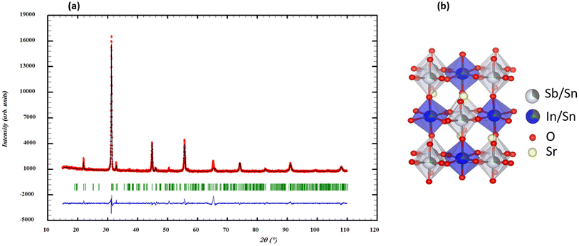
The stability of the crystal structure in Sr2(Sn0.33Sb0.33In0.33)2O6 was first evaluated by calculating the Goldschmidt tolerance factor (t) using the Shanon radius of the different elements (rSn4+ = 0.69 Å, rIn3+ = 0.80 Å, and rSb5+ = 0.60 Å).32 The calculated value of t = 0.958 suggests a possible reduction in symmetry.33 The reduced monoclinic symmetry (P21/c) results from the deformation of the ideal cubic perovskite, following a modification of the crystal structure by co-doping of Sn, In an Sb in Sr2(Sn0.33Sb0.33In0.33)2O6.33 The auto-indexing of the PXRD pattern of the sample using the DICVOL software from the FullProf suite34 reveals monoclinic symmetry with the following unit cell parameters: a = 5.450 Å, b = 5.720 Å, c = 9.700 Å and β = 123.53° as the best proposal. The search-match analysis using the ICDD PDF4+ database35 indicates that the double perovskite Sr2SbInO6 is the most suitable structural model for our compound, exhibiting monoclinic P21/c symmetry and lattice parameters consistent with those previously suggested by the DICVOL program, in agreement with the calculated t value of 0.958.34–36 During the Rietveld refinement, structural disorder within the octahedral sites was evidenced due to small variations in the radii of the cations within those sites (Fig. 1a). Consequently, a scenario was adopted for the distribution of Sb, In, and Sn cations, i.e. Sr2(In0.666Sn0.334) (Sb0.666Sn0.334)O6, considering a 1![[thin space (1/6-em)]](https://www.rsc.org/images/entities/char_2009.gif) :
:![[thin space (1/6-em)]](https://www.rsc.org/images/entities/char_2009.gif) 1 pseudo-ordering of the B cations in the Wyckoff sites 2a and 2d of P21/c (Fig. 1b). The results of the refinement in a monoclinic unit cell indicate a good agreement between calculated and observed patterns and the double perovskite structure is confirmed with good reliability factors (Table 1). The analysis of bond lengths in Table 2 shows that (Sn/Sb)–O distances, ranging from 1.94 to 1.98 Å, are more consistent with Sb5+ cation distances reported by Gagné, rather than Sb3+.37 However, our measured Sn/In–O distances are shorter, leading to BO32− octahedra. Co-substitution with Sn, In and Sb in the B sites results in distorted (Sn/Sb)O6 and (Sn/In)O6 octahedra, causing crystal deformation, structural defects and changes in electronic and conduction properties.
1 pseudo-ordering of the B cations in the Wyckoff sites 2a and 2d of P21/c (Fig. 1b). The results of the refinement in a monoclinic unit cell indicate a good agreement between calculated and observed patterns and the double perovskite structure is confirmed with good reliability factors (Table 1). The analysis of bond lengths in Table 2 shows that (Sn/Sb)–O distances, ranging from 1.94 to 1.98 Å, are more consistent with Sb5+ cation distances reported by Gagné, rather than Sb3+.37 However, our measured Sn/In–O distances are shorter, leading to BO32− octahedra. Co-substitution with Sn, In and Sb in the B sites results in distorted (Sn/Sb)O6 and (Sn/In)O6 octahedra, causing crystal deformation, structural defects and changes in electronic and conduction properties.
| Atom | Sites | x | y | z | Uiso |
|---|---|---|---|---|---|
| Sr | 4e | 0.24100 | 0.47400 | 0.24000 | 0.1051 |
| 0.334Sn/0.666Sb | 2a | 0.0 | 0.0 | 0.0 | 0.0555 |
| 0.334Sn/0.666In | 2d | 0.5 | 0.0 | 0.5 | 0.0941 |
| O1 | 4e | 0.17600 | 0.01060 | 0.23900 | 0.4618 |
| O2 | 4e | 0.31100 | 0.20110 | 0.02800 | 0.251 |
| O3 | 4e | 0.26170 | 0.73220 | 0.04000 | 0.1225 |
| Lattice parameters: a = 5.4502(3) Å, b = 5.72056(7) Å, c = 9.7006(7) Å and β = 123.53(1)°, RB(I) = 4.4886, χ2 = 2.0868 | |||||
| Distances | Exp. (Å) | Mean calc. (Å) | Relative error (%) |
|---|---|---|---|
| (Sn/In)–O1 | 2 × 2.1430(3) | 2.169 | 1.2 |
| (Sn/In)–O3 | 2 × 2.0393(1) | 2.145 | 4.1 |
| (Sn/In)–O2 | 2 × 2.0899(1) | 2.123 | 2.9 |
| (Sn/Sb)–O2 | 2 × 1.9395(2) | 2.046 | 7.1 |
| (Sn/Sb)–O1 | 2 × 1.9600(2) | 2.077 | 4.4 |
| (Sn/Sb)–O3 | 2 × 1.9800(1) | 2.068 | 4.5 |
To better understand the electronic structure of this new phase and confirm its structural properties, we decided to conduct further investigations using theoretical calculations with the GGA-PBE functional, along with all-electron Gaussian wave functions, implemented in the CRYSTAL23 software,27 as specified in the computational details section. To accurately replicate the experimental structure, we created a series of supercell models based on the most likely experimental model, the double perovskite P21/c. We also explored a triple perovskite model, also with P21/c symmetry, using the XRD data provided in Table S1.† Further details on the construction of these models and the results of structural relaxations can be found in the ESI (Table S1 and Fig. S1†). Table S1† shows that the double perovskite (O6) models exhibit greater stability compared to the triple perovskites (O9), with a small energy difference of 94 meV. We also note that the energies of all the considered double perovskite models are well below the thermal activation energy threshold of 25 meV. Although the possibility of polymorphism exists, it appears to be contrary to the potential for stabilization at high temperatures. The formation free energy calculations as a function of temperature, based on the double perovskite model and the reaction: SrSnO3 + Sr2SbInO6 → 3/2 Sr2(Sn0.33Sb0.33In0.33)2O6, clearly demonstrate that synthesis becomes feasible above 500 K (Fig. S2†). This strong correlation reinforces the validity of the experimentally proposed structural model and the statistical distribution of Sn/In and Sn/Sb across the 2d and 2a sites, emphasizing the significant configurational entropy at the B-sites. These findings provide solid evidence in support of the high-temperature stability of the new double perovskite phase.
Table S1† offers a comparative analysis of the experimental and theoretical average lattice parameters, including their relative errors. The results exhibit excellent congruence for the b, c, and β cell parameters, with discrepancies below 3.6%. However, the reproduction of the a parameter shows a larger deviation of 6%. To investigate this discrepancy, Table 2 contrasts the mean Sn/In–O and Sn/Sb–O bond lengths from the models with the experimental data. A general overestimation in the modeled distances compared to experimental predictions, possibly due to the functional employed is observed. A quite good alignment is seen for all Sn/In–O bonds, Sn/Sb–O1, and Sn/Sb–O3, with errors within 4.5%. Yet, the Sn/Sb–O2 bond length is notably overestimated (by 7%) in the calculations. This may be ascribed to the inherently challenging accurate positioning of oxygen atoms in Rietveld refinement, as oxygen's lighter atomic weight compared to elements like Sn, Sb, In, and Sr impacts the precision of their determined positions especially when defects or impurities are observed. The latter point will be further discussed below.
3.2. Crystallite size and microstrain
The Williamson–Hall method was employed to estimate the size of crystallites and lattice strain in the bulk. This method is expressed by the equation: β![[thin space (1/6-em)]](https://www.rsc.org/images/entities/char_2009.gif) cosθ = K × λ/D + 4ε
cosθ = K × λ/D + 4ε![[thin space (1/6-em)]](https://www.rsc.org/images/entities/char_2009.gif) sinθ, where β represents the full width at half maximum (FWHM) in radians, θ denotes the diffraction angle, λ stands for the X-ray wavelength, K is a shape constant (0.9), D indicates the crystallite size, and ε represents the micro-strain. In calculating the crystallite size, instrumental broadening was considered. An empirical linear equation was then applied to the experimental data. Utilizing the intercept and slope of this linear plot, the average crystallite size and micro-strain were determined in the annealed sample. The crystallite size was calculated to be 46 nm, and the lattice strain was measured at 1.15 10−3 (Fig. S3†). Interestingly, the micro-strain increased from 1.74 10−3 in SrSnO3 to 2.61 10−3 following the doping of Sn (+IV) with 5% In (+III)38 and subsequently decreased to 1.15 10−3 upon co-doping with In (+III) and Sb (+V) in Sr2(Sn0.33Sb0.33In0.33)2O6. These variations in strain values arise from differences in the ionic radii of the elements involved. Furthermore, an analysis of the scanning electron microscope (SEM) image (Fig. 2a) reveals the presence of a wide distribution of grains. This is due to agglomeration, which is the result of high sintering temperatures. The relative particle size histogram of the Sr2(Sn0.33Sb0.33In0.33)2O6 sample annealed at 1300 °C is displayed in Fig. 2a. To obtain statistics on grain sizes, Image J software was employed,39 and measurements were taken for at least 30 grains with size varying from 50 to 120 nm. The average grain size within the sample was estimated to be approximately 70 nm, a value somewhat higher than that determined by XRD analysis (46 nm). This discrepancy is attributed to the fact that the former reflects the size of aggregates, while the latter pertains to the size of coherent domains within the particles.40 By applying the relationship N = rSEM/rX-ray, we calculate the number of coherent diffraction domains within a particle. The results indicate that, on average, a particle comprises no more than 1.52 coherent diffraction domains. Table S2† presenting the EDX analysis results, reveals that the chemical composition of the compound closely aligns with the expected atomic percentages (Fig. 2b). The presence of carbon during the experimental analysis is likely due to the propensity of stannates to develop carbonates on their surfaces.41
sinθ, where β represents the full width at half maximum (FWHM) in radians, θ denotes the diffraction angle, λ stands for the X-ray wavelength, K is a shape constant (0.9), D indicates the crystallite size, and ε represents the micro-strain. In calculating the crystallite size, instrumental broadening was considered. An empirical linear equation was then applied to the experimental data. Utilizing the intercept and slope of this linear plot, the average crystallite size and micro-strain were determined in the annealed sample. The crystallite size was calculated to be 46 nm, and the lattice strain was measured at 1.15 10−3 (Fig. S3†). Interestingly, the micro-strain increased from 1.74 10−3 in SrSnO3 to 2.61 10−3 following the doping of Sn (+IV) with 5% In (+III)38 and subsequently decreased to 1.15 10−3 upon co-doping with In (+III) and Sb (+V) in Sr2(Sn0.33Sb0.33In0.33)2O6. These variations in strain values arise from differences in the ionic radii of the elements involved. Furthermore, an analysis of the scanning electron microscope (SEM) image (Fig. 2a) reveals the presence of a wide distribution of grains. This is due to agglomeration, which is the result of high sintering temperatures. The relative particle size histogram of the Sr2(Sn0.33Sb0.33In0.33)2O6 sample annealed at 1300 °C is displayed in Fig. 2a. To obtain statistics on grain sizes, Image J software was employed,39 and measurements were taken for at least 30 grains with size varying from 50 to 120 nm. The average grain size within the sample was estimated to be approximately 70 nm, a value somewhat higher than that determined by XRD analysis (46 nm). This discrepancy is attributed to the fact that the former reflects the size of aggregates, while the latter pertains to the size of coherent domains within the particles.40 By applying the relationship N = rSEM/rX-ray, we calculate the number of coherent diffraction domains within a particle. The results indicate that, on average, a particle comprises no more than 1.52 coherent diffraction domains. Table S2† presenting the EDX analysis results, reveals that the chemical composition of the compound closely aligns with the expected atomic percentages (Fig. 2b). The presence of carbon during the experimental analysis is likely due to the propensity of stannates to develop carbonates on their surfaces.41
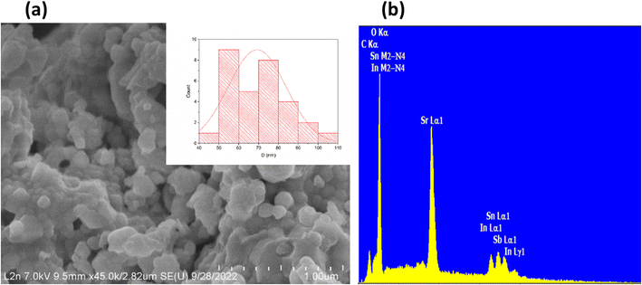 | ||
| Fig. 2 (a) SEM image (b) EDS spectrum of the Sr2(Sn0.33Sb0.33In0.33)2O6 perovskite, In insert particle size histogram (b) EDX spectra. | ||
3.3. FTIR and Raman spectroscopies
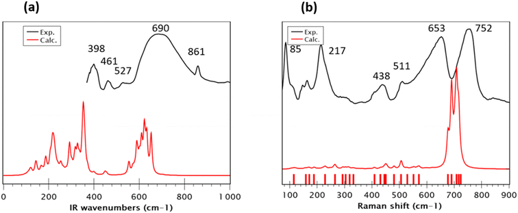
The FT-Infrared spectrum of Sr2(Sn0.33Sb0.33In0.33)2O6 was recorded at room temperature, covering the wavenumber range of 400–4000 cm−1. The modeling of the vibrational spectra (IR and Raman) of the new phase Sr2(Sn0.33Sb0.33In0.33)2O6, indicates that all its internal normal modes are located below 800 cm−1. For better clarity and to facilitate an effective comparison between theory and experiment, we limited the frequencies range in Fig. 3a. In the 550–750 cm−1 region of experimental spectrum, a broad absorption band is predominantly assigned to the antisymmetric stretching modes of the various BO32− octahedra (SnO32−, InO32− and SbO32−) in agreement with previously published findings.16,42,43 Moreover, both spectra exhibit similarities with those reported in the literature for SrSnO3.44 Experimental peaks at around ∼450 and ∼400 cm−1 reasonably correspond to the theoretical calculations at ∼450 and 325 cm−1, respectively. These normal modes are related to the bending of the O–B–O bonds. Interestingly, the calculated wavenumbers show a redshift compared to the experimentally observed frequencies, diverging from the usual overestimation typically seen when employing a harmonic potential. This discrepancy can be initially attributed to the previously noted overall overestimation of the B–O bond distances and, secondly, to the fact that the vibrational calculations were performed only at the Brillouin zone center, neglecting the dispersion effects near this point, even though supercell calculations somewhat account for disorder. The disordered metallic nature of the compound and the nanoscale crystallite size suggest significant dispersion impacting the broadness of the peaks. Furthermore, not accounting for the longitudinal-optical (LO) and transverse-optical (TO) splitting, which results from long-range coulombic interactions in the calculations, might contribute to these underestimated frequencies. Other perovskite variants like BaTiO3 and SrTiO3 often exhibit this phenomenon, which could account for the observed differences in our study.45 The experimental IR spectrum shows vibrations at 527, 859, 1070, 1468 and 1772 cm−1 (Fig. S4†), are likely due to the formation of carbonate groups during the calcination of SrCO3, as previously reported by Hong et al.46 The Raman spectral analysis of the Sr2(Sn0.33Sb0.33In0.33)2O6 compound (excitation wavelength 633 nm), depicted in Fig. 3b, provides critical insights into the perovskite's local structure.47 However, accurately assigning all vibrational modes in bulk samples remains a complex task. The Raman spectrum, recorded at room temperature alongside the calculated spectrum, reveals significant findings. In the high wavenumber region (>500 cm−1), two broad experimental bands at approximately 653 and 752 cm−1 correspond to theoretical modes at 717, 708, 703, 690, and 677 cm−1. This region is correlated with the breathing modes of the BO6 octahedra. The higher wavenumber modes (>700 cm−1) are primarily associated with the stretching of B–O bonds within the BO6 octahedra, particularly a main mix of Sn–O and In–O bonds. Modes in the range of 700–650 cm−1 are assigned to the stretching of Sb–O and Sn–O bonds. These modes are illustrated in Fig. S5.† The sequence of symmetric stretching modes appears to be more influenced by differences in effective mass than by bond length. Nevertheless, the comparison of this Raman spectrum with that of SrSnO3, as reported in the literature, which exhibits weak intensities in this region, suggests that the strong polarizability variations observed for this new phase are due to In–O and Sb–O bonds rather than Sn–O bonds.41,44 The mid-range frequencies (500–400 cm−1) combine stretching and bending motions, aligning with findings in related research.48 In the lower wavenumber region (<300 cm−1), the Raman spectrum displays long-range structural modes, with two prominent peaks at 217 and 85 cm−1, which are absent in the calculated spectrum. These low-frequency modes, as pronounced as the higher-frequency ones, bear resemblance to those seen in double rock salt perovskites.49,50 According to M. G. Masud et al.,51 these bands are indicative of the characteristic band patterns of the partially disordered monoclinic double perovskite structure. The experimental observation of these intense soft modes contrasts with their relatively muted presence in theoretical predictions. This discrepancy can be explained by the high polarizability calculated for Sb–O and In–O bonds, amplifying the intensity of harder modes and overshadowing the softer ones. The attribution of these modes to the presence of disorder is consistent with the fact that the Raman spectrum of a perfectly ordered model (model 8, Fig. S5†) also lacks these modes. It should also be noted that this model only exhibits just two intense hard modes, further confirming the synthesis of a disordered O6 model. Additionally, the nanometric particle size (40–70 nm), differing from the perfect crystal model in calculations, might introduce unaccounted surface effects, suggesting the need for a larger computational model for accurate depiction a task that is currently prohibitively expensive and challenging. Finally, the nanoscale particle size, in tandem with the presence of defects and metallic disorder, restricts phonon propagation, leading to broader Raman spectral bands. This is evidenced by an increased FWHM of these bands, similar to the phenomena observed in IR investigations. This analysis highlights the complex interplay between particle size, structural disorder and defect and their impact on the interpretations of the vibrational properties.3.4. UV-visible diffuse reflectance spectroscopy
The Kubelka–Munk function, denoted as F(R) and calculated from the diffuse reflectance data, is expressed as F(R) = (1 − R)2/2R ≈ K/S, where R represents the diffuse reflectance, and S and K stand for the scattering and absorption coefficients, respectively. The determination of the optical band gap (Eg) of Sr2(Sn0.33Sb0.33In0.33)2O6 was carried out using the Tauc model: (F(R) × hν)p = A(hν − Eg), with Eg representing the band gap energy, A being a constant, and the exponent p specifying the type of transition, which is 2 for a direct transition and 1/2 for an indirect transition. The band structure, as delineated in PBE (Fig. 4a), reveals a direct energy gap of 1.8 eV, consistent with the semiconductor characteristics of this phase. Additionally, according to the band structure, an indirect gap transitioning from X → Γ and occurs at 2.0 eV, approximately 200 meV higher. The density of state projection curves indicate electronic transitions predominantly from O2−(2p) to the unoccupied states of metals In, Sn, and Sb (Fig. 4b). These metals contribute comparably at the bottom of the conduction band. It is also observed that the M–O bonds exhibit a degree of covalence, evidenced by the presence of metal states in the valence band, along with a significant influence of indium states mingling with the oxygen band (Fig. 4b).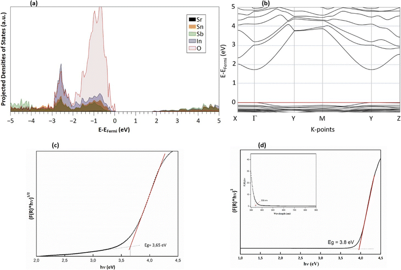 | ||
| Fig. 4 (a) Calculated band structure, (b) projected densities of states (PDOS), (c) Tauc plot for the indirect band gap and (d) direct band gap estimation from experimental reflectance data. | ||
The band gap energy (Eg) of Sr2(Sn0.33Sb0.33In0.33)2O6 is obtained through the extrapolation of the linear section of the [F(R) × hν]p plot. This analysis yields an optical band gap of 3.65 for indirect transition (Fig. 4c) and 3.8 eV for direct transition, which aligns with the Eopt value that calculated using the absorption edge's wavelength (Fig. 4d).52 The discrepancy between modeled and measured band gap is primarily due to the PBE-GGA functional, which is known to underestimate the measured optical gaps due to its poor treatment of exchange and correlation interactions.44,53 Nevertheless, regardless of the absolute value of the gap, and as noted earlier, the direct and indirect gaps in DFT are relatively close, with a difference of only ∼200 meV. This proximity may explain why UV measurements can be fitted to both direct and indirect gaps, with an observed difference of approximately 300 meV. Although DFT may underestimate the absolute value of the band gap, it accurately describes the relationship between the two types of gaps, offering valuable insights into the material's electronic structure. In light of these results, one can conclude that this property makes it a promising candidate for technological applications, given its classification as a wide-gap non-magnetic insulator.
3.5. Complex impedance analysis
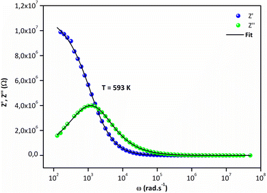
Fig. 5a and (b) report the frequency dependence of real Z′ and imaginary Z′′ impedance plots at various temperatures. It is observed in Fig. 5a that Z′ diminishes with enhancing temperature at lower frequencies, indicating an increase in the alternating current (AC) conductivity and the NTCR behavior.54 At higher frequencies (f > 104 kHz), the values of Z′ merge for all temperatures. Z′ is temperature-independent, which signifies the release of space charges in the material.55 The dependence of the imaginary impedance (Z′′) as the function of frequency for different temperatures well illustrates the charge transport mechanism and the relaxation mode in Sr2(Sn0.33Sb0.33In0.33)2O6 at different temperatures (Fig. 5b). The relaxation process appears to be influenced by immobile charge carriers at low temperatures and defects/vacancies at high temperatures. As the temperature increases, a shift of the relaxation peak occurs towards higher frequencies indicating a thermally dependent relaxation mechanism. Furthermore, the magnitude of this peak decreases consequently, suggesting a decrease in grain resistance with temperature. The width of the relaxation peak in Z′′ indicates the possibility of a distribution of relaxation times (Fig. 6).56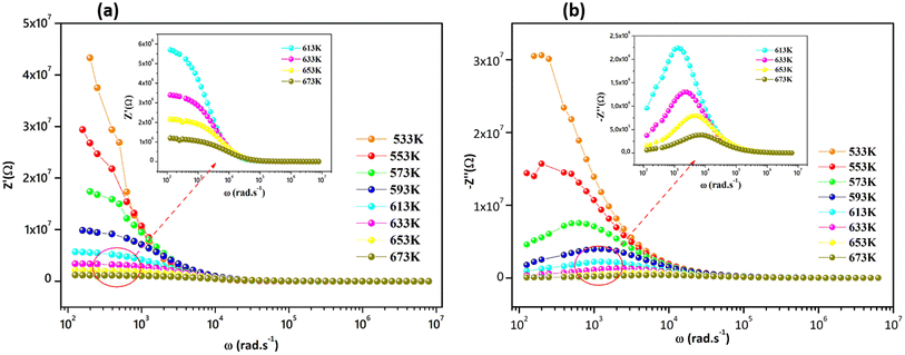 | ||
| Fig. 5 (a) Variation of real part, and (b) variation of imaginary part of impedance with angular frequency at several temperatures. | ||
Fig. 7 displays the Cole–Cole plots (Z′′ vs. Z′) at various temperatures. A semicircular arc with a center below the Z′ axis is displayed in every plot. The temperature-dependent poly-dispersive character of dielectric relaxation in non-Debye behavior in Sr2(Sn0.33Sb0.33In0.33)2O6 is confirmed by the tilt parameter α in the Cole–Cole diagram, which quantifies the distribution of relaxation durations, being non-zero. The majority of relaxors are complex perovskite structures with two or more ions in the A- and B-sub-lattices having complete or partial abnormalities.57 The material contribution coming from a parallel combination of grain capacitance (Cg), constant phase element (CPE1), and resistance (R) to grain can be responsible for high-frequency semicircular arcs. Values (R, Cg, Q, and α) obtained from an experimental fit of the data are displayed in Table S3.† Fig. 7 depicts the corresponding electrical circuit. The insert's graphical depiction demonstrates how resistance R drops as temperature rises, this behavior is characteristic with negative temperature coefficient of resistance (NTCR) compounds widely used as thermistors, i.e. temperature sensors in industrial and medical domains because of their high-temperature sensitivity, durability, and cheap.58,59
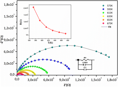 | ||
| Fig. 7 Nyquist plot of Sr2(Sn0.33Sb0.33In0.33)2O6 at different temperatures and equivalent circuit of fitting data for the system. The resistance plot as a function of temperature in inset. | ||
3.6. AC conductivity study
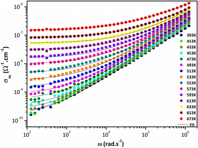
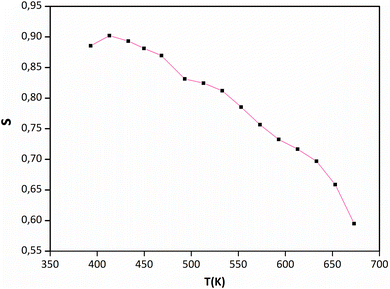
Fig. 8 shows temperature and frequency variations of the sample's conductivity. AC conductivity corresponds to the frequency dispersion zone, which is shifts to higher frequencies and at higher temperature, corresponds to the DC conductivity.56 As the temperature increases, the DC conductivity value increases, indicating that the sample exhibits semiconductive behavior (Fig. 8).Jonscher's universal power law explained by σac(ω) = σdc + AωS is a useful model for describing the conduction process in dielectric materials, especially in terms of their alternating current conductivity. A is a constant influenced by temperature, ω represents angular frequency, “s” signifies the level of interaction among mobile charge carriers and their environment, and σdc refers to direct current conductivity. Fig. 9 portrays the connection between the temperature and the frequency exponent “s”. Within the temperature range of 400 to 473 K, the exponent remains consistently around 0.9. This pattern is indicative of conduction through tunneling without the need of thermal activation. The value of “s” remains stable during this period and then gradually decreases before experiencing a more pronounced decline. This reduction occurs in two phases: a subtle one between 473 and 593 K, followed by a more substantial drop between 593 and 673 °C. This suggests that in this material, the grain conduction phenomenon aligns with the correlated barrier hopping (CBH) behavior.60
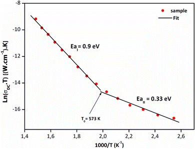
The DC conductivity of the sample was related to temperature by the transformed equation: Lnσdc = Lnσ0 + [−Ea/(1000/T)]. Fig. 10 indicates an Arrhenius-type conduction in the temperature range 393–673 K. As shown in the Sr2(Sn0.33Sb0.33In0.33)2O6, the temperature dependency indicates two conduction mechanisms that are active in the sample. The activation energy is 0.33 eV at low temperature and 0.9 eV at high temperature. As above mentioned in the electrical study section, the dielectric loss factor reaches its maximum at this same critical temperature when the transition from one section to the next is noticed. Such a low activation energy value results from the connection between the polarons breaking and migrating freely as the temperature rises more. A shift in the charge carrier from a single to a double polaron, or from a small to a large one can account for the change in the slope at 573 K.
3.7. Modulus analysis
Fig. 11, displays how the angular frequency affects the real part of the electrical modulus (M′) and the imaginary part (M′′) at various temperatures. At lower temperatures, M′(ω) follows a less dispersed pattern, almost appearing linear.61 However, as the temperature increases, M′(ω) starts to display a dispersive behavior, where the value of M′ increases and reaches a maximum saturation point at different temperatures (Fig. 11a and b). When looking at lower frequencies, the low values of M′ indicate the absence of electrode and/or ionic polarization effects and suggest the migration of polarons over longer distances due to the slow reversal of the electrical field. From 593 K onwards, the behavior of M′′ displays a broad peak. The shape of the M′′(ω) curves implies a relaxation process with a shift towards higher frequencies with increasing temperature, indicating the thermally activated nature of the relaxation time.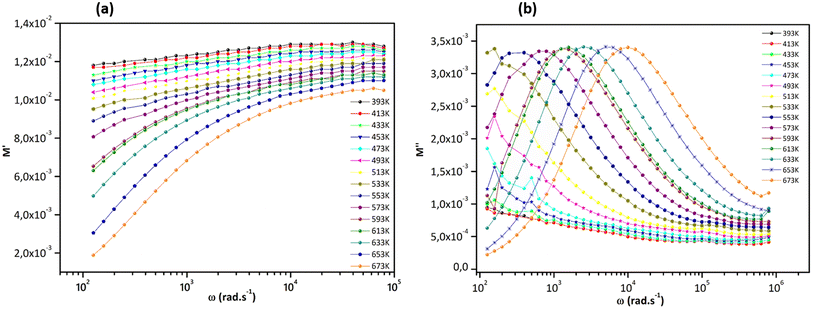 | ||
| Fig. 11 (a) Dependence of M′ and (b) M′′ of Sr2(Sn0.33Sb0.33In0.33)2O6 versus frequency at different temperatures. | ||
4. Conclusion
A transparent semiconductor perovskite oxide, Sr2(Sn0.33Sb0.33In0.33)2O6, was synthesized via solid-state reaction and subjected to comprehensive experimental and theoretical analyses to assess its structural, microstructural, optical, vibrational, electronic, and dielectric properties. XRD and EDX results confirmed the excellent crystalline quality and accurate elemental composition of the prepared sample. DFT–PBE calculations, through extensive structural, thermodynamic, and vibrational studies, validated the synthesis and structural refinement of this new phase, classifying it as a double perovskite crystallizing in the P21/c space group. Experimental UV-visible measurements demonstrated high optical transparency across a broad spectral range, with an indirect bandgap of 3.65 eV, supported by theoretical calculations.According to DOS curves, electronic transitions predominantly occur from O2− (2p) to the unoccupied states of In, Sn, and Sb, indicating the material's potential for optoelectronic applications. Further insight into the conduction mechanism was gained by analysing the frequency-dependent behaviour of σac for grain response, using Jonscher's universal power law at different temperatures. This analysis revealed that correlated barrier hopping is the predominant conduction mechanism. The temperature dependence of DC conductivity indicated two distinct conduction mechanisms, with activation energies of 0.33 eV and 0.9 eV below and above T = 573 K, respectively. Finally, electric modulus analysis confirmed the presence of dielectric relaxation. The observed decrease in resistance with increasing temperature aligns with the overall findings, suggesting that this material could be a promising candidate for high-temperature thermistor applications, relying on the NTCR (Negative Temperature Coefficient of Resistance) effect.
Data availability
The data that support the findings of this study are available on request from the corresponding author, Besma BELGACEM upon reasonable request.Author contributions
Besma Belgacem: carried out material preparation, collection and data analysis and paper draft. Nabil Nasri: carried out the preparation of the material, and data optical analysis. Mouna Ben Yahia: drafted the theoretical section, participated in discussions, results interpretation, and manuscript revision. Abderrazek Ouslati: participated in impedance measurements, results' discussion and manuscript revision. Rached Ben Hassen: was responsible for the methodology, data curation, writing, visualization, validation and supervision. All authors have read and approved the final manuscript.Conflicts of interest
The authors declare that they have no known competing financial interests or personal relationships that could have appeared to influence the work reported in this paper.Acknowledgements
Financial support from the Ministry of Higher Education and Scientific Research of Tunisia is gratefully acknowledged. The authors gratefully acknowledge the ICDD for financial support (Grant number: 09–04). The authors thank Dr Akram Alhussein, Université de Technologie de Troyes, Pole Technologique Sud Champagne, France for scanning electron microscope (SEM) measurements, energy dispersive X-ray (EDX) measurements. The authors thank Pr. Hammadi Khemekhem, University of Sfax, Faculty of Science of Sfax for the Raman measurements. The authors appreciate Ms. Hajer REBAI for linguistic editing and proofreading of the manuscript.References
- A. R. F. A. Teixeira, A. de Meireles Neris, E. Longo, J. R. de Carvalho Filho, A. Hakki and D. Macphee, et al., SrSnO3 perovskite obtained by the modified Pechini method—Insights about its photocatalytic activity, J. Photochem. Photobiol., A, 2019, 369, 181–188 CrossRef CAS.
- L. Chantelle, A. L. Menezes de Oliveira, B. J. Kennedy, J. Maul, M. R. S. da Silva and T. M. Duarte, et al., Probing the Site-Selective Doping in SrSnO3: Eu Oxides and Its Impact on the Crystal and Electronic Structures Using Synchrotron Radiation and DFT Simulations, Inorg. Chem., 2020, 59(11), 7666–7680 CrossRef CAS PubMed.
- B. Hadjarab, A. Bouguelia and M. Trari, Synthesis, physical and photo electrochemical characterization of La-doped SrSnO3, J. Phys. Chem. Solids, 2007, 68(8), 1491–1499 CrossRef CAS.
- H. He, Z. Yang, Y. Xu, A. T. Smith, G. Yang and L. Sun, Perovskite oxides as transparent semiconductors: a review, Nano Convergence, 2020, 7(1), 32 CrossRef CAS.
- S. Barouni, A. Brahmia, H. Chaker, M. M. Maslov, A. Alhussein and R. B. Hassen, First-principles prediction of half metallic-ferromagnetism in La0.25Sr0.75Sn0.4In0.25Ru0.35O3 and enhanced experimental electrical and magnetic behaviours, Phys. Chem. Chem. Phys., 2024, 26(26), 18102–18112 RSC.
- Q. Liu, J. Dai, X. Zhang, G. Zhu, Z. Liu and G. Ding, Perovskite-type transparent and conductive oxide films: Sb- and Nd-doped SrSnO3, Thin Solid Films, 2011, 519(18), 6059–6063 CrossRef CAS.
- Q. Liu, F. Jin, G. Gao and W. Wang, Ta doped SrSnO3 epitaxial films as transparent conductive oxide, J. Alloys Compd., 2017, 717, 62–68 CrossRef CAS.
- J. Kim, H. Yun, J. Seo, J. H. Kim, J. H. Kim and K. A. Mkhoyan, et al., Deep-UV Transparent Conducting Oxide La-Doped SrSnO3 with a High Figure of Merit, ACS Appl. Electron. Mater., 2022, 26(7), 3623–3631 CrossRef PubMed.
- M. Kumar Mahapatra, P. Singh, D. Kumar and O. Parkash, Synthesis, crystal structure, microstructure and electrical behaviour of systems Sr1−x Lax SnO3 and SrSn1−x Nix O3 (X ≤ 0·10), Adv. Appl. Ceram., 2006, 105(6), 280–284 CrossRef.
- M. A. Sattar, M. Benkraouda and N. Amrane, First-principles investigation on the structural, electronic, vibrational and magnetic properties of the Co-substituted orthorhombic SrSnO3, Phys. B, 2020, 590, 412216 CrossRef CAS.
- B. Raveau, The Perovskite History More than 60 Years of Research from the Discovery of Ferroelectricity to Colossal Magnetoresistance via High TC Superconductivity, Solid State Chem., 2007, 35, 171–173 CrossRef CAS.
- A. L. Ben, B. Belgacem, J. S. Filhol, M. L. Doublet, M. B. Yahia and R. Ben Hassen, New p-type Al-substituted SrSnO3 perovskites for TCO applications?, Chem. Commun., 2020, 56(17), 2566–2569 RSC.
- K. I. Kobayashi, T. Kimura, H. Sawada, K. Terakura and Y. Tokura, Room-temperature magnetoresistance in an oxide material with an ordered double-perovskite structure, Nature, 1998, 395(6703), 677–680 CrossRef CAS.
- M. A. Amin, G. Nazir, Q. Mahmood, J. Alzahrani, N. A. Kattan and A. Mera, et al., Study of double perovskites X2InSbO6 (X = Sr, Ba) for renewable energy; alternative of organic-inorganic perovskites, J. Mater. Res. Technol., 2022, 18, 4403–4412 CrossRef CAS.
- A. Zouaghi, B. Belgacem, A. Alhussein, A. Brahmia and R. Ben Hassen, Study of the structural, optical, and electrical characteristics of Sr2Sn1.6In0.2Cu0.2O6−δ mixed ionic-electronic conductor, J. Solid State Chem., 2023, 328, 124303 CrossRef CAS.
- B. Belgacem, M. M. Maslov, S. Kaya, I. H. Ali and R. Ben Hassen, Crystal chemistry, DFT calculation and optical properties of the double perovskite stannate Sr2Sn0.8In0.8W0.4O6, J. Mol. Struct., 2022, 1259, 132716 CrossRef CAS.
- L. Li, X. Li, W. Xia, Y. Wang, F. Ling and S. Jiang, et al., Investigation on the optical sensing behaviors in single Eu3+-activated Sr2InSbO6 phosphors under green light excitation, J. Alloys Compd., 2022, 906, 164322 CrossRef CAS.
- Y. Xie, X. Geng, J. Guo, W. Shi, Q. Lv and J. Kong, et al., Luminescence of a novel double-perovskite Sr2InSbO6: Eu3+ orange-red-emitting phosphor for white LEDs and visualization of latent fingerprints, Mater. Res. Bull., 2022, 146, 111574 CrossRef CAS.
- M. Zhao, S. Liu, F. Zhao, H. Cai, Z. Song and Q. Liu, Cr3+-doped double perovskite antimonate, efficient and tunable phosphors from NIR-I to NIR-II, Inorg. Chem. Front., 2022, 9, 4602–4607 RSC.
- D. Liu, G. Li, P. Dang, Q. Zhang, Y. Wei and L. Qiu, et al., Highly efficient Fe3+-doped A2BB′O6 (A = Sr2+, Ca2+; B, B′ = In3+, Sb5+, Sn4+) broadband near-infrared-emitting phosphors for spectroscopic analysis, Light: Sci. Appl., 2022, 27(1), 112 CrossRef.
- M. Y. Sofi and D. C. Gupta, Scrutinized the inherent spin half-metallicity and thermoelectric response of f-electron-based RbMO3 (M = Np, Pu) perovskites: a computational assessment, Sci. Rep., 2022, 12, 19476 CrossRef CAS PubMed.
- M. Y. Sofi, M. S. Khan and J. Ali, et al., Exploring the lead-free halide Cs2MGaBr6 (M = Li, Na) double perovskites for sustainable energy applications, Sci. Rep., 2024, 14, 5520 CrossRef CAS PubMed.
- M. Y. Sofi, M. S. Khan and J. Ali, et al., Unlocking the role of 3d electrons on ferromagnetism and spin-dependent transport properties in K2GeNiX6 (X = Br, I) for spintronics and thermoelectric applications, J. Phys. Chem. Solids, 2024, 112022 CrossRef CAS.
- P. Hohenberg and W. Kohn, Inhomogeneous Electron Gas, Phys. Rev., 1964, 136(3B), B864–B871 CrossRef.
- W. Kohn and L. J. Sham, Self-Consistent Equations Including Exchange and Correlation Effects, Phys. Rev., 1965, 140(4A), A1133–A1138 CrossRef.
- J. P. Perdew, K. Burke and M. Ernzerhof, Generalized Gradient Approximation Made Simple, Phys. Rev. Lett., 1996, 28(18), 3865–3868 CrossRef PubMed.
- A. Erba, J. K. Desmarais, S. Casassa, B. Civalleri, L. Donà and I. J. Bush, et al., CRYSTAL23: A Program for Computational Solid State Physics and Chemistry, J. Chem. Theory Comput., 2023, 24(20), 6891–6932 CrossRef.
- J. Grant Hill, Int. J. Quantum Chem., 2013, 113, 21–34 CrossRef.
- M. Ferrero, M. Rérat, R. Orlando and R. Dovesi, The calculation of static polarizabilities of 1-3D periodic compounds. the implementation in the crystal code, J. Comput. Chem., 2008, 29(9), 1450–1459 CrossRef CAS.
- M. Ferrero, M. Rérat, R. Orlando and R. Dovesi, Coupled perturbed Hartree–Fock for periodic systems: the role of symmetry and related computational aspects, J. Chem. Phys., 2008, 7(1), 014110 CrossRef.
- M. Ferrero, M. Rérat, B. Kirtman and R. Dovesi, Calculation of first and second static hyperpolarizabilities of one- to three-dimensional periodic compounds. Implementation in the CRYSTAL code, J. Chem. Phys., 2008, 28(24), 244110 CrossRef PubMed.
- R. D. Shannon, Revised effective ionic radii and systematic studies of interatomic distances in halides and chalcogenides, Acta Crystallogr., Sect. A: Cryst. Phys., Diffr., Theor. Gen. Crystallogr., 1976, 32(5), 751–767 CrossRef.
- B. E. Day, N. D. Bley, H. R. Jones, R. M. McCullough, H. W. Eng and S. H. Porter, et al., Structures of ordered tungsten- or molybdenum-containing quaternary perovskite oxides, J. Solid State Chem., 2012, 185, 107–116 CrossRef CAS.
- J. Rodriguez-Carvajal. FULLPROF: a program for Rietveld refinement and pattern matching analysis, in Satellite Meeting on Powder Diffraction of the XV Congress of the IUCr, Toulouse, France, 1990 Search PubMed.
- S. N. Kabekkodu, J. Faber and T. Fawcett, New Powder Diffraction File (PDF-4) in relational database format: advantages and data-mining capabilities, Acta Crystallogr., Sect. B: Struct. Sci., Cryst. Eng. Mater., 2002, 58(Pt 3 Pt 1), 333–337 CrossRef PubMed.
- W. T. Fu and D. J. W. IJdo, X-ray and neutron powder diffraction study of the monoclinic perovskites Sr2MSbO6 (M = In, Y), Solid State Commun., 2005, 134(3), 177–181 CrossRef CAS.
- O. C. Gagné and F. C. Hawthorne, Bond-length distributions for ions bonded to oxygen: metalloids and post-transition metals, Acta Crystallogr., Sect. B: Struct. Sci., Cryst. Eng. Mater., 2018, 1(1), 63–78 CrossRef.
- T. Mohan, S. Kuppusamy and R. J. V. Michael, Tuning of Structural and Magnetic Properties of SrSnO3 Nanorods in Fabrication of Blocking Layers for Enhanced Performance of Dye-Sensitized Solar Cells, ACS Omega, 2022, 7(22), 18531–18541 CrossRef CAS PubMed.
- C. A. Schneider, W. S. Rasband and K. W. Eliceiri, NIH Image to ImageJ: 25 years of image analysis, Nat. Methods, 2012, 9(7), 671–675 CrossRef CAS PubMed.
- M. Sukumar, L. John Kennedy, J. Judith Vijaya, B. Al-Najar and M. Bououdina, Facile microwave assisted combustion synthesis, structural, optical and magnetic properties of La2−xSrxCuO4 (0 ≤ x ≤ 0.5) perovskite nanostructures, J. Magn. Magn. Mater., 2018, 465, 48–57 CrossRef CAS.
- M. C. F. Alves, M. R. Nascimento, S. J. G. Lima, P. S. Pizani, J. W. M. Espinosa and E. Longo, et al., Influence of synthesis conditions on carbonate entrapment in perovskite SrSnO3, Mater. Lett., 2009, 63(1), 118–120 CrossRef CAS.
- S. Ouni, S. Nouri, H. Khemakhem and R. Ben Hassen, Phase transitions, dielectric properties, and vibrational study of stannates perovskites Sr1−xErxSnO3−δ, Mater. Res. Bull., 2014, 51, 136–140 CrossRef CAS.
- C. Bharti and T. P. Sinha, Dielectric properties of rare earth double perovskite oxide Sr2CeSbO6, Solid State Sci., 2010, 4, 498 CrossRef.
- E. Moreira, J. M. Henriques, D. L. Azevedo, E. W. S. Caetano, V. N. Freire and E. L. Albuquerque, Structural, optoelectronic, infrared and Raman spectra of orthorhombic SrSnO3 from DFT calculations, J. Solid State Chem., 2011, 1(4), 921–928 CrossRef.
- L. L. Rusevich, G. Zvejnieks, E. A. Kotomin, M. M. Kržmanc, A. Meden and Š. Kunej, et al., Theoretical and Experimental Study of (Ba, Sr)TiO3 Perovskite Solid Solutions and BaTiO3/SrTiO3 Heterostructures, J. Phys. Chem. C, 2019, 31(4), 2031–2036 CrossRef.
- J. Hong, S. J. Heo and P. Singh, Water mediated growth of oriented single crystalline SrCO3 nanorod arrays on strontium compounds, Sci. Rep., 2021, 9(1), 3368 CrossRef PubMed.
- A. P. Ayala, I. Guedes, E. N. Silva, M. S. Augsburger, C. del, M. Viola and J. C. Pedregosa, Raman investigation of A2CoBO6 (A = Sr and Ca, B = Te and W) double perovskites, J. Appl. Phys., 2007, 15(12), 101 Search PubMed.
- V. L. Vilesh and G. Subodh, Crystal structure and dielectric properties of BaANaTeO6 (A = Bi, La) double perovskites, Ceram. Int., 2017, 15(15), 12718–12723 CrossRef.
- S. A. Prosandeev, U. Waghmare, I. Levin and J. Maslar, First-order Raman spectra of First-order Raman spectra of AB′1/2B′′1/2O3 double perovskites, Phys. Rev. B, 2005, 71(21), 214307 CrossRef.
- A. Dias, G. Subodh, M. T. Sebastian, M. M. Lage and R. L. Moreira, Vibrational Studies and Microwave Dielectric Properties of A-Site-Substituted Tellurium-Based Double Perovskites, Chem. Mater., 2008, 8(13), 4347–4355 CrossRef.
- M. G. Masud, H. Sakata, A. K. Biswal, P. N. Vishwakarma and B. K. Chaudhuri, Structural, ac conductivity scaling and magnetodielectric behaviour of a partially disordered insulating ferromagnetic double perovskite Eu2NiMnO6, J. Phys. D: Appl. Phys., 2015, 48(37), 375504 CrossRef.
- M. Z. M. Halizan, Z. Mohamed and A. K. Yahya, Understanding the structural, optical, and dielectric characteristics of SrLaLiTe1−xMnxO6 perovskites, Sci. Rep., 2021, 7(1), 9744 CrossRef PubMed.
- P. Borlido, et al., Exchange-correlation functionals for band gaps of solids: benchmark, reparametrization and machine learning, npj Comput. Mater., 2020, 6, 96 CrossRef CAS.
- R. Das and R. N. P. Choudhary, Dielectric relaxation and magneto-electric characteristics of lead-free double perovskite: Sm2NiMnO6, J. Adv. Ceram., 2019, 1(2), 174–185 CrossRef.
- O. Bidault, P. Goux, M. Kchikech, M. Belkaoumi and M. Maglione, Space-charge relaxation in perovskites, Phys. Rev. B, 1994, 15(12), 7868–7873 CrossRef.
- D. K. Mahato, A. Dutta and T. P. Sinha, relaxation and ac conductivity of double perovskite oxide Ho2ZnZrO6 Dielectric, Phys. B, 2011, 1(13), 2703–2708 CrossRef.
- A. K. Singh, S. K. Barik, R. N. P. Choudhary and P. K. Mahapatra, Ac conductivity and relaxation mechanism in Ba0.9Sr0.1TiO3, J. Alloys Compd., 2009, 24(1), 39–42 CrossRef.
- A. Feteira, Negative Temperature Coefficient Resistance (NTCR) Ceramic Thermistors: An Industrial Perspective, J. Am. Ceram. Soc., 2009, 92(5), 967–983 CrossRef CAS.
- B. K. Das, T. Das, K. Parashar, S. K. S. Parashar, R. Kumar and H. K. Choudhary, et al., Investigation of structural, morphological and NTCR behaviour of Cu-doped ZnO nanoceramics synthesized by high energy ball milling, Mater. Chem. Phys., 2019, 1, 419–429 CrossRef.
- R. Mukherjee, S. Saha, A. Dutta and T. P. Sinha, Dielectric and Raman spectroscopic studies of A2ErSbO6 (A = Ba, Sr and Ca), J. Alloys Compd., 2015, 5, 222–229 CrossRef.
- I. M. Hodge, M. D. Ingram and A. R. West, Impedance and modulus spectroscopy of polycrystalline solid electrolytes, J. Electroanal. Chem. Interfacial Electrochem., 1976, 74, 125–143 CrossRef CAS.
Footnote |
| † Electronic supplementary information (ESI) available. See DOI: https://doi.org/10.1039/d4ra05308g |
| This journal is © The Royal Society of Chemistry 2024 |

