DOI:
10.1039/D4RA05784H
(Paper)
RSC Adv., 2024,
14, 33751-33763
Fabrication of heterostructure multilayer devices through the optimization of Bi-metal sulfides for high-performance quantum dot-sensitized solar cells
Received
9th August 2024
, Accepted 7th October 2024
First published on 24th October 2024
Abstract
In this work, a titanium dioxide and lead sulfide (TiO2/PbS) nano-size heterostructure with tin sulfide was fabricated and coated via a two-step direct deposition process. Its microstructure, morphology, elemental composition, optical absorption, and photochemical activity were investigated. Linear sweep voltammetry and cyclic voltammetry curves substantiated its catalytic activity, indicating quantum dot effects of a well-developed space charge domain on the surface of the hybrid structure. These give rise to electron–hole recombination suppression and a high charge mobility rate. Moreover, direct stabilization was identified in current density, corresponding to the hybrid structures limiting the diffusion current process. Higher JSC values observed were substantiated by the role of quantum dot-size effects and enhanced crystalline structures, leading to a reduction in series resistance and an improved conversion efficiency of 10.05%. Overall, theoretical analyses and empirical findings indicated that the seamless migration of photoexcited electrons across the interfaces of SnS and PbS is linked to quantum dot effect synergy. This is facilitated by the space charge region, which serves as a conduit for efficient electron transfer between the respective materials.
Introduction
The need for clean energy sources to mitigate the impact of global climate change has made clean energy conversion devices such as solar photovoltaic (PV) cells a highly sought-after solution.1–3 Third-generation solar cells such as dye-sensitized solar cells (DSSCs) have emerged with tremendous prospects because of their easy fabrication, low cost, realistic power conversion efficiencies, environmental friendliness, and ease of sandwich build-up.3–6 To improve the conversion efficiencies of DSSCs in the past two decades, studies have been carried out with stable and efficient modern dyes, fast electron transfer, excellent photon scattering ability, and a new high-surface-area photoanode electrode.7–9 Organic sensitizers have shown pathways for highly efficient electron transfer, which is important for DSSCs for donating and accepting electrons, along with their good chemical, photochemical, and long-term stability.10 To further enhance the efficiency of this technique, great attention has been paid to conventional liquid electrolytes with over 14% power conversion efficiency (PCE).11 To achieve the theoretical values of 44% in practical applications of DSSCs, semiconductor quantum dot (QD) engineering is of great importance in increasing the PCE of quantum dot-sensitized solar cells (QDSSCs). Tin sulfide (SnS) is another interesting material whose I–V measurements with several metals form a Schottky and ohmic contact in Al–SnS–In and Ag–SnS–In systems.3,12 SnS is chemically stable, nontoxic, naturally abundant, cheap, and easy to fabricate, making it suitable for QDSSC applications.13–15 Moreover, its high absorption coefficient and optical band gap (<2 eV) with a p-type nature give rise to better charge migration, which is crucial for QDSSC devices.16 Moreover, according to density functional theory calculations, SnS has emerged as a highly useful material in QDSSCs and hydrogen production.3,17
Previous studies have shown that higher efficiencies can be achieved by combining QDs with other materials.18,19 Nanostructure materials such as Sb2S3, PbS, CdSe, PbSe, and CdS have been used as absorbers in QDSSCs. Among these semiconductors, lead sulfide (PbS) QDs have a tunable band gap of 0.41 eV with a high absorption coefficient and could be explored as co-absorbers with other metal sulfides such as SnS to enhance the PCE of QDSSCs.18 This is because the theoretical efficiency, multiple excitons, and quantized discrete band structures that are above the Shockley–Queisser limit are in favour of PbS absorbers.20 The low performance of PbS absorbers in QDSSCs as compared with other metal sulfide QD materials21,22 paves the way for more studies on the development and exploration of PbS with other semiconductors. The passivation of the PbS layer directly above the SnS-absorber surface of the TiO2 electrode can reduce the photoinjected recombination of electrons with the polysulfide electrolyte and improve the PCE of QDSSCs.19 This PCE can be achieved by combining PbS and SnS via step-wise modification of band-edge levels.23
Several established deposition techniques such as thermal evaporation,24 atomic layer deposition,25 electrochemical deposition,26 chemical vapor deposition,27 sputtering,28 chemical bath deposition,29 spray pyrolysis,30 and E-beam evaporation31 have been reported for the coating of SnS and PbS semiconductors onto the surface of TiO2 electrode substrates. All the above-mentioned approaches are not cost-effective because they suffer from slow deposition rates or vacuum-based technology. Presently, most attention is focused on the fabrication of nanostructure materials through optimization to form uniform sizes and shapes since their physicochemical and optoelectronic properties are strongly influenced by the optimization. Therefore, the formation of controlled metal sulfide nanostructures with good optoelectronic properties will benefit both the PCE QDSSCs and their commercialization.31 The single-source precursor (SSP) approach is one of the most attractive, cost-friendly, and large-scale production, which is accurate and easy to control, with additional benefits over metal sulfide nanostructured fabrication. Herein, we report on the indirect loading of PbS and SnS solution-process-controlled synthesis of semiconductor metal sulfides nanostructured using SSPs on the surface of TiO2 glass substrates in QDSSCs.
Experimental
Materials and methods
All chemical reagents are of high-purity grade, and were used as received from Sigma Aldrich. Ligands such as N-butyldithiocarbamate and N-dodecyldithiocarbamate were synthesized according to the procedure earlier reported in ref. 32. The following chemicals were purchased: methanol, oleic acid, tin(II) chloride dihydrate (Cl2Sn·2H2O (https://www.ereztech.com/product/stannous-chloride-dihydrate-10025-69-1/)), oleylamine (ODE), tri-n-octylphosphine oxide (TOPO), ammonium, carbon disulfides (CS2), diethyl ester, butylamine, and dodecylamine. Bis(N-diisopropyl-N-octyldithiocarbamato) (OCT) Pb(II) complexes were obtained from Merck, which has been reported in our previous study.22 Testing kits containing fluorine-doped tin oxide (FTO) platinum electrode (drilled) (size: 20 × 20 mm; active area: 6 × 6 mm), TiO2 FTO electrode (opaque) (size: 20 × 20 mm; active area: 6 × 6 mm), Iodolyte HI-30 polysulfide electrolyte, gaskets, masks, and hot seal were purchased from Solaronix. Water, PbS and SnS nanoparticles were obtained from dithiocarbamate molecular precursors.
[Dodecyldtc] yield: 11.6789 g (69.80%) 1H NMR (DMSO) δ 3.23 (s, 2H–NH), 0.82 (t, 3H–CH3), 1.53–1.56 (s, 2H–CH2), 1.25–1.38 (s, 1H-SH). 13C NMR (DMSO) δ 22.6–26.3 (–CH2), 198 (–CS2), 14.4 (–CH3), 45.2 (–C–NH). Selected IR (cm−1) 1412 v(C–N), 1218 v(C–S), 3454 v(N–H), 2936 v(CH3). UV-vis (CH3OH solution, nm): 236. [Butyldtc] yield: 5.3103 g (93.33%) 1H NMR (DMSO) δ 3.24–3.33 (s, 2H–NH),0.87 (t, 3H–CH3), 1.65–2.51 (s, 2H–CH2), 1.28 (s, 1H-SH). 13C NMR (DMSO) δ 19.7–29.5 (–CH2), 198.5 (–CS2), 13.6 (–CH3), 44.9 (–C–NH). Selected IR (cm−1) 1485 v(C–N), 1097 v(C–S), 3276 v(N–H), 2908 v(CH3). UV-vis (CH3OH solution, nm): 369.
Synthesis of bis(N-butyl-N-dodecyldithiocarbamato)Sn(II) complexes [Dodec-buthyldtc] (1)
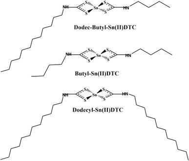
The complexes were synthesized following the procedure previously reported in ref. 33 with slight modification, as shown in Scheme 1. N-Butyldithiocarbamate and N-dodecyldithiocarbamate ligands (0.4158 g, 2.5 mmol and 0.6964 g, 2.5 mmol) were each dissolved separately in 15 mL of distilled water. Sncl2·2H2O salts (0.5641 g, 2.5 mmol) were then mixed in a ratio of 1/1/1 together with continuous stirring for 2 h. The mixtures gave rise to yellow precipitates, which were filtered and thoroughly rinsed with cold methanol and dried. Formulated as [Sn(Dodec-butyldtc)]: (C18H38N2S4Sn) yield: 3.7091 g (46.23%) 1H NMR (DMSO) δ 3.25–3.68 (s, 2H–NH), 0.85–0.92 (t, 3H–CH3), 1.55–1.64 (s, 2H–CH2), 1.25–1.38 (s, 1H-SH). 13C NMR (DMSO) δ 19.6–31.8 (–CH2), 200 (–CS2), 13.6–14.4 (–CH3), 39.2 (–C–NH). Selected IR (cm−1) 1515 v(C–N), 944 v(C–S), 3408 v(N–H), 580 v(M–S), 2851 v(CH2), 2918 v(CH3). UV-vis (CH3OH solution, nm): 280. Same steps were followed for single ligands: N-butyldithiocarbamate and N-dodecyldithiocarbamate with Sncl2·2H2O salts in ratio 2/1 and formulated as [Sn(Dodecyldtc)] and [Sn(Butyldtc)]. [Sn(Dodecyldtc)] (2) (C26H50N2S4Sn) yield: 3.5284 g (44.12%) 1H NMR (DMSO) δ 3.65–3.68 (s, 2H–NH),0.87–0.92 (t, 3H–CH3), 2.51–2.76 (m, 2H–CH2), 1.28–1.65 (s, 1H-SH). 13C NMR (DMSO) δ 19.7–31.7 (–CH2), 201 (–CS2), 13.6–14.2 (–CH3), 40 (–C–NH). Selected IR (cm−1) 1517 v(C–N), 936 v(C–S), 3306 v(N–H), 541 v(M−S), 2851 v(CH2), 2919 v(CH3). UV-vis (CH3OH solution, nm): 293. [Sn(Butyldtc)] (3) (C10H20N2S4Sn) yield: 2.0176 g (33.16%) 1H NMR (DMSO) δ 3.23–3.65 (s, 2H–NH),0.84–0.92 (t, 3H–CH3), 1.53–1.56 (s, 2H–CH2), 1.24–1.25 (s, 1H-SH). 13C NMR (DMSO) δ 22.6–31.8 (–CH2), 200 (–CS2), 14.4 (–CH3), 40 (–C–NH). Selected IR (cm−1) 1503 v(C–N), 1232 v(C–S), 3173 v(N–H), 406–611 v(M–S), 2843 v(CH2), 2927 v(CH3). UV-vis (CH3OH solution, nm): 280.
 |
| | Scheme 1 Structures of Sn(Dodec-butyldtc), Sn(Dodecyldtc) and Sn(Butyldtc) complexes. | |
Formation of tin sulfide SnS nanoparticles
The synthesis of SnS was done with slight modifications in line with the procedure already reported in the literature.32,33 First, 0.2 g of [Dodec-butyldtc] (1) was dispersed in 4 mL of oleylamine and TOPO in a three-necked bottom flask (250 mL). The resulting mixture was degassed for 10 min at about 20–30 °C, heated up to 250 °C and then maintained for 1 h in an inert atmosphere. Afterwards, the resulting solution was obtained by naturally cooling to 70 °C followed by the addition of 30 mL of methanol for the precipitation of the SnS nanoparticles. The obtained precipitates were washed severally with methanol and centrifuged to obtain the final end product as SnS nanoparticles, which is labelled as SnS1. Similar steps were taken for [Dodecyldtc] (2) and [Butyldtc] (3), labelled as SnS2 and SnS3. The bis(N-diisopropyl-N-octyldithiocarbamato) Pb(II) complex was used to synthesize PbS as reported previously.22
Fabrication of QDSCS
The TiO2 electrode was soaked in 0.010 g PbS dissolved in 10 mL of distilled water for 24 hours, rinsed with distilled water, and then soaked in 0.010 g SnS in 10 mL of distilled water for 24 hours. The sensitized FTO-TiO2/PbS/SnS films were used as photoanodes, with a FTO-Pt film as the counter electrode. The Iodolyte HI-30 electrolyte solution was injected between the photoanode and counter electrode through a siphonic effect. The QDSSC device was assembled as TiO2/PbS/SnS/HI-30/Pt with an active area of 6 × 6 mm for the three devices. The assembled devices were sealed under a hot press and labelled as P/S#1, PS#2, and PS#3. To the best of our knowledge, both materials synthesized from these molecular precursors have not been reported as co-absorbents in QDSCs. These parameters were used to calculate the conversion efficiency (%) of the prepared devices using eqn (1)–(4):
The efficiency of the cells developed in this work was estimated using eqn (1)–(5):5
| |
 | (1) |
| |
 | (2) |
| |
 | (3) |
| |
 | (4) |
| | |
FFideal = Pmax/JLidealVOCideal
| (5) |
Pmax is the maximum power density as:
P(
V) =
VxP(
V) curve.
Physical characterizations
X-ray diffraction was performed within a rotation anode high-power X-ray diffractometer (XRD) (Bruker D8 Advance) with Cu-Kα radiation (k = 1.5406 Å) at 40 kV and 40 mA. Surface morphology and the chemical constituents of the fabricated DSSC cells were analyzed by field emission scanning electron microscopy and X-ray energy-dispersive spectroscopy using FESEM, JEOL, JSM-6700F, 5 kV with a Nanotrace EDX detector (Thermo Electron) and transmission electron microscopy (TEM, JEOL JEM-2010) at 200 kV. Functional group identification was achieved by Fourier transform infrared (FTIR) spectroscopy using a PerkinElmer Spectrum 1. The optical properties of the cells were measured using a UV-visible and PL spectrometer by Perkin Elmer-Lamda 45. We measured the surface's roughness at a scan rate of 0.8 Hz using an atomic force microscope (JPK NanoWizard II AFM, JPK). Keithley 2400 with Source Meter (AM) 1.5G (1000 Wm−2) was used to measure the IV properties of the as-prepared devices. A Gamry 10101E electrochemical workstation equipped with a three-electrode device was employed to evaluate the electrocatalytic performance of the three samples. The electrochemical impedance spectra (EIS) were analyzed while operating at a frequency range of 1 Hz–107 Hz at 10 mV. Cyclic voltammetry (CV) and linear sweep voltammetry (LSV) analyses were performed at scan rates of 100 and 10 mV s−1. Chronoamperometry (CA) was evaluated to study the effect of passivation on the stability of the cells.
Results and discussion
AFM and SEM for SnS quantum dot photon absorbers
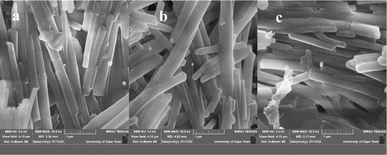
Fig. 1a–f display the AFM images of 2-D and 3-D for the three samples. The obtained values for the surface roughness are 324 nm, 408 nm and 454 nm for SnS1, SnS2 and SnS3 respectively. The increases in the surface roughness can be linked to the quantum-sized effects.34 The low surface roughness is due to the increase in size distribution. Moreover, the optical properties and conversion efficiency of QDSCs rest on the low surface roughness. Fig. 2a–c reveal the morphology of the samples where SnS nano-rods with smooth surfaces are densely packed together with a good crystal feature for all the samples. SEM micrographs follow a similar trait as with the AFM results obtained in this study.35,36 Co-absorbance of PbS and SnS nanorods blend into an electron transporting layer like TiO2 is important for solar cell applications and allows for fast electron transport at the electrolyte interface.
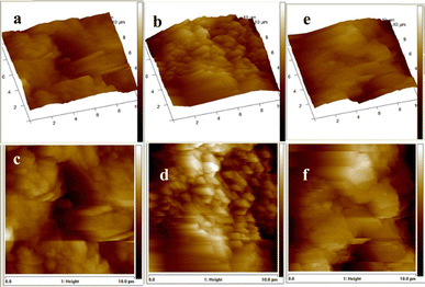 |
| | Fig. 1 Three- and two-dimensional AFM images of SnS1 (a and c), SnS2 (b and d) and SnS3 (e and f) nanoparticles. | |
 |
| | Fig. 2 SEM images of SnS1 (a), SnS2 (b) and SnS3 (c) nanoparticles. | |
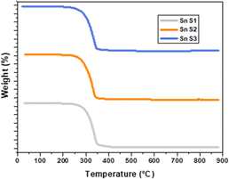
The thermal stability of SnS was identified by thermogravimetric (TGA) analysis, as shown in Fig. 3. The stability of the SnS QDs was found at 354–362 °C, with complete loss of organic species from the structure of the molecular precursor, as reported in our previous work.4 The high thermal stability of SnS makes it a potential material for the effective optimization of various optoelectronic properties, which pave the way for their applications and improved conversion efficiency obtained in the present study.
 |
| | Fig. 3 TGA analysis of SnS1, SnS2 and SnS3 nanoparticles. | |
XRD, Raman and FTIR spectra of P/S#1, P/S#2, and P/S#3
The structure of the prepared devices was characterized using an XRD instrument, as illustrated in Fig. 4a. The Crystal Impact software was used for the identification and quantification of phase indexes and the elemental weights of the assembled electrodes as shown in Table 1. The XRD peaks show the preferential orientation of the modified cells, which corresponds with JCPDS card no. 96-152-7227 for orthorhombic SnS. This is oriented to the (110), (131), (002) and (112) directions for SnS. The XRD peaks for PbS agree with the (200), (210), (310), (311), and (314) orientations with JCPDS card no. 96-901-4779 for orthorhombic PbS. These agree with the literature report in ref. 37 and 38. To further assess the crystalline quality, phase, and dopant information of the FTO electrodes, Raman spectroscopy measurements were employed for the P/S#-1, P/S#-2, and P/S#-3 modified cells, as seen in Fig. 4b. Raman peaks at 264 cm−1 and 420 cm−1 indicate the presence of PbS, which is consistent with the observed vibrational shifts reported previously.39 These peaks are ascribed to the phonon mode of first-order LO and the two-phonon scattering 2LO mode.38 A sharp lattice vibration peak at 158 cm−1 and small vibrations at 209 cm−1 are indexed to the SnS phase of Ag and B3g vibration modes.40,41 The presence of a known mode relies on incidence and scattering radiation directions parallel to any of the three axis (a, b, c), scattered photons, and the electrical polarization of the incidence.41,42 The functional groups of the modified devices as P/S#1, P/S#2, and P/S#3 FTIR spectra are shown in Fig. 4c.
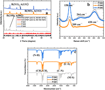 |
| | Fig. 4 XRD patterns (a), Raman spectra (b) and FTIR spectra (c) of P/S#1, P/S#2 and P/S#3 modified devices. | |
Table 1 XRD parameters for P/S#1, P/S#2, and P/S#3 devices with orthorhombic (B) PbS and orthorhombic (A) SnS phases
| Samples |
2θ (deg.) |
FWHM (deg.) |
Miller indices (hkl) |
Crystallite size (nm) |
Amounts calculated using the reference intensity ratio |
| Phase index amount (%) |
Element amount (weight%) |
| P/S#1 |
20.76 |
0.1050 |
B (200) |
80.37 |
SnS 34.4, PbS 65.6 |
Pb |
Sn |
S |
| 22.68 |
0.1050 |
A (110) |
80.63 |
56.8 |
27.1 |
16.1 |
| 25.78 |
0.2100 |
B (210), A (002) |
40.55 |
| 33.42 |
0.1575 |
B (301) |
55.03 |
| 37.67 |
0.2625 |
B (311), A (131) |
33.41 |
| 51.42 |
0.2100 |
B (303), A (112) |
43.87 |
| |
|
|
|
Average 55.64 |
|
|
|
|
| P/S#2 |
26.15 |
0.2625 |
B (210), A (002) |
32.45 |
SnS 44.7, PbS 55.3 |
47.9 |
35.2 |
16.9 |
| 37.30 |
0.2625 |
B (311), A (131) |
33.37 |
| 51.42 |
0.2100 |
B (303), A (112) |
43.87 |
| |
|
|
|
Average 36.56 |
|
|
|
|
| P/S#3 |
26.64 |
0.2625 |
B (002), A (002) |
32.50 |
SnS 41.6, PbS 58.4 |
50.6 |
32.7 |
16.7 |
| 37.83 |
0.2625 |
B (311), A (131) |
33.43 |
| 51.61 |
0.2100 |
B (303), A (112) |
43.91 |
| |
|
|
|
Average 36.61 |
|
|
|
|
In the three devices, the ν(C–N) bands were detected at 1470, 1536, and 1633 cm−1, while the band at 964 cm−1 corresponds to ν(C–S). The strong peaks at 2918 and 2851 cm−1 for P/S#1, P/S#2, and P/S#3 are ascribed to the asymmetric CH3 and CH2 correlated with the capping agent of hexadecylamine. The ν(N–H) bands observed at 3257 cm−1 are assigned to the hexadecylamine vibrations.43 The ν(M–S) peaks at 730, 578, and 413 cm−1 were assigned to the Sn–S and Pb–S of the metal and sulfur ions. The FTIR studies indicate the successful loading of SnS and PbS on TiO2, which is confirmed by the presence of titanium, oxygen, and carbon in the EDS spectra.4,20,44
HRTEM images of P/S#1, P/S#2, and P/S#3
The interfacial activities of the TiO2/PbS/SnS/HI-30/Pt-modified electrodes were studied by high-resolution transmission electron microscopy. The devices were examined by HRTEM, as seen in Fig. 5a–l. The HRTEM images presented in Fig. 5a, d and g display hexagonal shapes for P/S#1, P/S#2, and P/S#3 devices, which consist of the deposition of PbS and SnS on the TiO2. The HRTEM images of P/S#1, P/S#2, and P/S#3 devices indicate a high crystallinity heterostructure of TiO2/PbS/SnS. The lattice spacing and their crystalline plane for the three devices are (303) and 0.32 nm for P/S#1, (002), (301) and 0.33 nm for P/S#2, and (002), (301), (314) and 0.33 nm for P/S#3, to the orthorhombic PbS and SnS (JCPDS data 96-901-4779 and 96-152-7227). The selected area electron diffraction (SAED) pattern corresponds to the PbS and SnS (SAED) pattern in the inserted Fig. 5d, h and l shows the apparent ring diffraction pattern comes from the cubic PbS and hexagonal SnS crystalline nature. The average particle sizes are 4.03 nm, 5.18 nm, and 6.97 nm. The average particle size distribution of SnS QDs was found within 2.22–17.11 nm, while PbS QDs reveal a grain size average of 1.82–5.95 nm.4,22 The size distribution shows that the average particle size is within the quantum dot region.45
 |
| | Fig. 5 HRTEM image (a, d, and g), lattice spacing (b, e, and h) and SAED pattern (c, f, and i) of P/S#1, P/S#2 and P/S#3 modified devices. | |
SEM, AFM and EDS images of P/S#1, P/S#2, and P/S#3
Fig. 6d–l show the SEM, AFM and EDS images of the P/S#1 device, displaying a polyhedral morphology.46 The microstructure of the TiO2 films changed after the deposition of the binary structure of PbS/SnS, as seen in Fig. 6b, for the P/S#2 device. The porosity of the P/S#3 cell decreased with the addition of PbS and SnS. SnS covered the surface of the PbS cell and filled in the pores generated by TiO2 particle packing.47 The elemental composition of P/S#1, P/S#2, and P/S#3 modified devices is studied by the EDS images illustrated in Fig. 6m–o. The uniform distribution of elements in P/S#1 and P/S#2 devices was confirmed in comparison to the P/S#3 device. Atomic force microscopic (AFM) images of the multilayer devices are displayed in Fig. 6a–c. A detailed analysis of the surface profile of the three modified cells in terms of root mean square (RMS) and average roughness (Ra) was obtained. The smooth topography has RMS roughness values of 31.2 nm, 29.6 nm, and 29.9 nm, while the Ra values are around 23.3–24.5 nm for P/S#1, P/S#2, and P/S#3, respectively. This is an indicator of the role of both PbS and SnS quantum dot size effects of the modified cells, which account for their high current density and electron transfer speed, supported by the EIS and the I–V results.
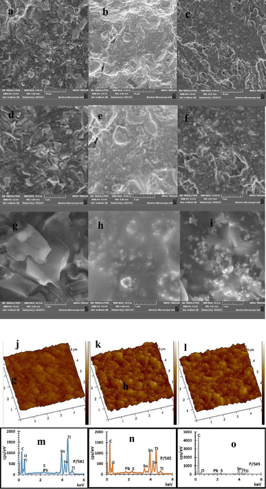 |
| | Fig. 6 AFM images (a–c), SEM images (d–l) and EDS spectra (m–o) of P/S#1, P/S#2 and P/S#3 modified devices. | |
UV-vis and Tauc plot spectra of P/S#1, P/S#2, and P/S#3
The optical properties of P/S#1, P/S#2, and P/S#3 are presented in Fig. 7a by the UV-vis absorption spectrum. P/S#3 reveals a high intensity with an absorption edge over the entire range. This can be linked to the relatively narrow band gap of PbS and SnS. It is worth noting that P/S#2 has a similar absorption edge with less intensity compared to the P/S#1 cell device. Moreover, both P/S#2 and P/S#3 cell devices display absorption covering the entire visible region. The relation of (ahv)2 vs. hv could be obtained by calculating the UV-vis data, as shown in Fig. 6b. The empirical Tauc formula is as follows:where hv stands for the energy of the incident photon and the absorption coefficient, where A and n are constants. The Eg value of the three samples could be valued from the (ahv)2 hv curves by the extrapolating method. Eg of P/S#3 at 2.75 eV and P/S#3 has the values at 2.0 eV and 1.0 eV as first and last order, while that of P/S#1 at 2.5 eV, confirming the heterostructure combination of TiO2/PbS/SnS, which are closely related to the previous studies by ref. 48–50. The spectral response falls in the visible regions for the blue shift, which agrees with the HRTEM quantum dot size distribution; this area is beneficial for the enhancement of the photochemical response under visible light.51,52 Moreover, these results are supported by the J–V results of this study. To further assert the optical properties of the produced cells, PL analysis was performed at an excitation wavelength of 350 nm, as shown in Fig. 7c and d. This is an important technique for understanding the recombination of electron–hole photogenerated in P/S#1, P/S#2, and P/S#3 devices. Emissions are detected in the blue region at 410–460 nm for three samples confirming their quantum-sized effects. These emissions correspond to defects and emission bands; radiation decays from the conduction band to the valence band. A decrease in P/S#2 and P/S#3 intensity was associated with a slower recombination rate and increased charge separation, which correlate with the EIS observation. This occurrence also suggests that there is multiple exciton generation from the absorber (PbS and SnS), which may generate more than one electron–hole pair for each absorbed photon with energy at least twice that of the absorber band gap. The high intensity observed in P/S#1 indicates that electrons are not excited more efficiently from the VB to the CB. This inference implies that the cells have lower photocatalytic activity and charge separation compared to P/S#2 and P/S#3 which is supported by the I–V results in this study.
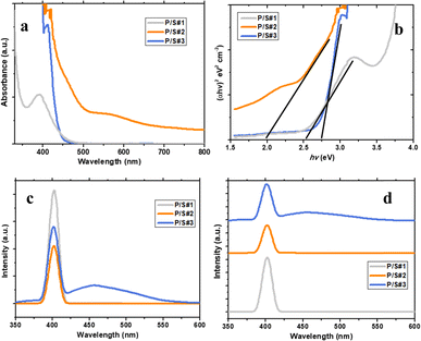 |
| | Fig. 7 UV-vis absorption spectra (a), Tauc plot (b), PL spectra (c) and PL spectra superimposed (d) of P/S#1, P/S#2 and P/S#3 modified devices. | |
EIS and Bode plot analysis of P/S#1, P/S#2, and P/S#3
To understand the electron activity at the interfaces of P/S#1, P/S#2, and P/S#3, the EIS analysis was performed, as seen in Fig. 8a. For all devices (compositions), the diameter of the semicircular impedance spectrum (high-frequency time-constant region) is considerably comparative to the electron-transfer resistance at the electrode–electrolyte interface, revealing the kinetics of charge transfer from the redox reaction at the electrode–electrolyte interface. The Nyquist plots for the 3 devices and the equivalent circuit model used in fitting the parameters are shown in Fig. 8a–d and Table 2. The models used in describing the Nyquist and Bode plots are similar to those reported in the literature.53,54
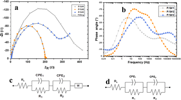 |
| | Fig. 8 EIS Nyquist plot (a), Bode plot (b) and equivalent model circuit (c) for P/S#1, P/S#3 and (d) P/S#2 modified devices. | |
Table 2 EIS fitted parameters for P/S#1, P/S#2 and P/S#3 devicesa
| Parameters |
P/S#1 |
P/S#2 |
P/S#3 |
| LSV and CV curves of P/S#1, P/S#2, and P/S#3. |
| Rs (Ω) |
2.745 |
1.667 |
1.501 |
| R1 (Ω) |
56.640 |
16.308 |
12.317 |
| R2 (Ω) |
375.489 |
200.514 |
310.659 |
| σ (Ω/s1/2) |
— |
— |
0.0015 |
The overall impedance, ZT, of the Nyquist plots of P/S#1 and P/S#2 in Fig. 8a is given by eqn (7), while that of P/S#3 is given by eqn (8).
| | |
ZT = Rs + R1‖ZCPE1 + R2‖ZCPE2
| (7) |
| | |
ZT = Rs + R1‖ZCPE1 + R2‖ZCPE2 + Zw
| (8) |
where
Rs is the series resistance of the cell and is evaluated from the real impedance axis shift of the Nyquist plot from the origin,
ZCPE1 and
ZCPE2 describe the impedance to mobile charge carriers from the different bulk transport layers of the specimen. From
eqn (8) Zw, represents the slow diffusion process observed on P/S#3 as an incomplete arc starting at an approximate angle of 45°.
55 This region of the Nyquist plot is commonly referred to as Warburg region. The Warburg element's impedance was calculated as follows:
| |
 | (9) |
where
σ is the Warburg coefficient defined as follows:
| |
 | (10) |
where
D represents the diffusion coefficient, and
R,
T and
F are the ideal gas constant, absolute temperature, and Faraday constant respectively. Subscripts “
O” and “
R” represent the oxidation and reduction species. “
C” and “
D” are the concentration and diffusivities of the species, while “
n” is the number of electrons transferred.
The EIS response of the P/S#1 and P/S#3 devices, as shown in Fig. 8a, supplies information about the bi-metal layer electrode and the carrier selective layer in terms of their charge transport.55 The modified hybrid device of P/S#2 reveals an arc with a smaller radius, illustrating a higher transport efficiency, which is in agreement with the disparity of shunt resistance (Rsh) and the series resistance (Rs) lower value as an indicator of better transport performance. P/S#2 devices show a heterojunction hybrid structure of PbS and SnS QD distributed layers of TiO2/PbS/SnS/HI-30, which is favorable for carrier transport.56 This implies that bimetal with quantum dots size is additive with the hybrid anode, which reduces non-radiative recombination more efficiently. Therefore, it improves current density with a better effect on electron transport in the conduction band of the hybrid anode. A Bode phase plot is a characteristic tool with the ability to indicate the predominant electrical behavior of a device at a given frequency range. It provides easier visualization of the different electron diffusion processes (time-constants). Fig. 8b shows the Bode phase plots of the three devices. The Bode plot of P/S#1 first knee observed and P/S#3 more evident are linked to the capacitive–resistive transition.57 The plots show lower capacitive characteristics than that of P/S#2 caused by a more resistive PbS/electrolyte interface as well as the high porosity of the SnS. This suggests that the co-absorbent of PbS and SnS improves charge transfer while inhibiting charge recombination. The increase in JSC, which can be observed in Table 4 J–V parameter, supports the P/S#2 and P/S#3 devices. This is further confirmed by the AFM and LSV results. The Bode plot for the P/S#2 device indicates a highly capacitive device acting as an efficient cooperative bi-metal material.57
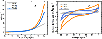
Fig. 9a and b show the Linear Sweep Voltammetry (LSV) curves of P/S#1, P/S#2, and P/S#3 modified devices at a scan rate of 10 mV s−1. The PbS-coupled SnS binary heterostructure current density for P/S#3 devices is higher than that of P/S#1 and P/S#2 devices within the measured potential range. The P/S#1 and P/S#2 low current density could be linked to a large band gap, resulting in poor response in charge transfer ability, which can be correlated with the Tauc plot result in Fig. 7b. The improved P/S#3 hybrid structure agrees with the band gap narrowing ability of chalcogenides SnS and PbS, as seen in the Tauc plot. This combination benefits from being able to reduce the band gap, leading to the entire absorption of the solar cell spectrum and synergistic interaction between both metal sulphides, thus creating better paths or conduits for effective interfacial charge transfer. This also implies that the quantum dot size effect plays a vital role in the formation of heterostructure metal sulfides and the higher current density obtained by P/S#2 and P/S#3 modified devices in comparison to P/S#1. Moreover, a higher surface area promotes more active sites, increases the transport rate of photoinduced charge carriers, and notably increases the efficiency of the catalyst, which accounts for the observed enhancement by P/S#2 and P/S#3 devices. These LSV results elucidated the influence of lower band gaps on the P/S#2 and P/S#3 modified devices, which is favorable for efficient and better mobility of charge carriers and photogenerated charge carrier separation for improved conversion output.58 The electrochemical properties were taken using the potential window and scan rate as stated above for the LSV to analyse the cyclic voltammetry (CV) curves of P/S#1, P/S#2, and P/S#3 modified devices. Fig. 9b confirms the catalytic behaviors of the three cells. P/S#3 and P/S#2 devices show a better current density response as compared to the P/S#1 device, implying a well-developed space charge region at the surface of the binary hybrid structure. These give rise to electron–hole recombination suppression and a high charge mobility rate. Moreover, the easy flow of photogenerated electrons through SnS and PbS quantum dot superior synergy and the space charge region produced channels for the electronic transfer of electrons between them, which led to improved conversion efficiency. Therefore, the electrocatalytic and photocatalytic performance of the modified devices is linked to the high active surface area and quantum size of the binary heterostructure.58
 |
| | Fig. 9 LSV curves (a) and CV curve (b) of P/S#1, P/S#2 and P/S#3 modified devices. | |
CA and I–V analysis of P/S#1, P/S#2, and P/S#3
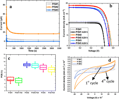
Fig. 10a and Table 3 display the chronoamperograms of P/S#1, P/S#2, and P/S#3-modified devices. The three samples show the gradual increase in current density with time until reaching a maximum (Imax, tmax), represented using the Cottrell eqn (11).| |
 | (11) |
where i(t) is the current, n is the number of electrons transferred, F is Faraday's constant, A is the electrode surface area,  is the diffusion coefficient,
  is the initial concentration, and t is the time. The rise in the current portion relates to a new phase of development through the increasing number of nuclei, while the final is caused by the flow of diffusion ions to the surface of the working electrode to stabilize the change in potential. The growing nuclei of the binary hybrid structures form successive overlapping and diffusion regions around themselves under mass transfer, leading to a planar surface corresponding to tmax and the later decay in current density as a function of time. Instant decay is observed in P/S#3 modified devices, while direct stabilization is identified in the current density values of P/S#1 modified devices, corresponding to the binary hybrid structures limiting the diffusion current process.59 Moreover, the Imax for the P/S#2 cells is longer than that of the P/S#1 device, which could be justified by the size distribution of quantum dot variation and the growth kinetics of the binary hybrid structures.60 An additional procedure to identify the impact of binary structure on the photovoltaic properties of P/S#1, P/S#2, and P/S#3 modified devices by taking their J–V measurement is seen in Fig. 10b. The solar cell parameters JSC, VOC, FF, and η are shown in Fig. 10b and Table 4. The increase in JSC observed in P/S#2 and P/S#3 devices is due to their small quantum dot-sized and better crystallinity, leading to a reduction in series resistance in the modified cells. The decrease in VOC observed in P/S#1 is caused by Eg reduction in SnS and shunt resistance in the modified device. According to this result, the electrocatalytic ability of Iodolyte HI-30 polysulfide electrolyte ions and the related device performances might be directly influenced by the elemental proportion of bimetal on the TiO2/PbS/SnS electrodes. This is largely anchored on the molecular precursor variation of PbS and SnS paving the way for the effective optimization of optoelectronic properties. The high JSC and the P/S#2 and P/S#3 devices' electrochemical performance correlate with the bimetal phase and elemental ratio, which is consistent with other studies61–64 with improved electrocatalytic characteristics. Better electrocatalytic activity and favorable surface morphology interactions with the Iodolyte HI-30 polysulfide electrolyte ions resulted in greater JSC for P/S#2 and P/S#3.65–67 The high efficiency of 9.99–8.95% reported in the present study is significantly higher than that reported in previous research studies that used co-sensitization, including Li et al. (8.72%),68 Xu et al. (8.28%),69 and Yang and Zhong (7.24%),70 as seen in Table 5.
 |
| | Fig. 10 Chronoamperograms (a), I–V curve (b), PCE (c) and multi-cycle CV test (d) of P/S#1, P/S#2 and P/S#3 modified devices. | |
Table 3 Maximum parameters (Imax, tmax) for P/S#1, P/S#2 and P/S#3 devices
| Parameters |
P/S#1 |
P/S#2 |
P/S#3 |
| Imax (mA cm−2) |
2.7 |
18 |
0.9 |
| tmax (s) |
311 |
411 |
0.2 |
Table 4 I–V parameters for P/S#1, P/S#2 and P/S#3 devices
| Samples |
VOC (V) |
JSC (mA cm−2) |
FF |
η (%) |
Pmax (W) |
| P/S#1 |
0.64 ± 00 |
11.4 ± 01 |
0.81 ± 01 |
5.90 ± 01 |
5.97 |
| P/S#1 F 24 h |
0.64 ± 01 |
10.8 ± 01 |
0.82 ± 02 |
5.67 ± 02 |
5.67 |
| P/S#2 |
0.77 ± 00 |
19 ± 02 |
0.68 ± 01 |
9.95 ± 01 |
10.05 |
| P/S#2 F 24 h |
0.73 ± 02 |
19 ± 02 |
0.72 ± 03 |
9.99 ± 01 |
10.03 |
| P/S#3 |
0.76 ± 01 |
18 ± 01 |
0.69 ± 00 |
9.44 ± 02 |
9.45 |
| P/S#3 F 24 h |
0.72 ± 03 |
18 ± 02 |
0.69 ± 01 |
8.95 ± 01 |
8.86 |
Table 5 Previously reported I–V parameters in the literature on co-sensitizationa
| Samples |
VOC (V) |
JSC (mA cm−2) |
FF |
η (%) |
Ref. |
| TW = this work. |
| ZnO/NR@/ZnO/IO/CdS/CdSe |
0.66 |
38.60 |
0.44 |
11.24 |
71 |
| TiO2/ZCISe |
0.59 |
26.43 |
0.56 |
8.72 |
68 |
| TiO2/CdS/CdSe |
0.62 |
32.29 |
0.40 |
8.28 |
69 |
| TiO2/CdS/CdSe NS |
0.58 |
15.07 |
0.51 |
4.42 |
72 |
| TiO2/CuInS2 |
0.68 |
11.33 |
0.41 |
3.13 |
73 |
| TiO2/CdS/CdSe |
0.572 |
15.8 |
0.59 |
5.28 |
74 |
| TiO2/CdTe/CdSexS1−x |
0.62 |
16.58 |
0.69 |
7.24 |
70 |
| TiO2/CdS/CdSe/ZnSe |
0.58 |
20.11 |
0.55 |
6.39 |
75 |
| TiO2/CdS/CdSe |
0.66 |
14.39 |
0.60 |
5.70 |
76 |
| TiO2/CdTe/CdS/CdS |
0.61 |
20.19 |
0.51 |
6.32 |
77 |
| TiO2/CdS/CdSe |
0.60 |
14.98 |
0.54 |
4.85 |
78 |
| TiO2/CdSe/CdS |
0.42 |
13.46 |
0.41 |
2.31 |
79 |
| TiO2/CdS/CdSe |
0.59 |
14.23 |
0.55 |
4.62 |
80 |
| P/S#1 |
0.64 ± 00 |
11.4 ± 01 |
0.81 ± 01 |
5.90 ± 01 |
TW |
| P/S#1 F 24 h |
0.64 ± 01 |
10.8 ± 01 |
0.82 ± 02 |
5.67 ± 02 |
TW |
| P/S#2 |
0.77 ± 00 |
19 ± 02 |
0.68 ± 01 |
9.95 ± 01 |
TW |
| P/S#2 F 24 h |
0.73 ± 02 |
19 ± 02 |
0.72 ± 03 |
9.99 ± 01 |
TW |
| P/S#3 |
0.76 ± 01 |
18 ± 01 |
0.69 ± 00 |
9.44 ± 02 |
TW |
| P/S#3 F 24 h |
0.72 ± 03 |
18 ± 02 |
0.69 ± 01 |
8.95 ± 01 |
TW |
Eqn (12) compares the incident photon-to-current conversion efficiency (IPCE) measurement values for the best-performing devices that were collected between 350 and 800 nm.64
| |
 | (12) |
where
I stands for the incident light power at
λ, and
JSC is the measured short circuit current in the device. The P/S#2 device's IPCE value, which was 57% at 410 nm, was higher than that of the P/S#3 device, which was 54% at 410 nm, and the P/S#1 device, which produced an IPCE value of 34% at 410 nm. Because of better light absorption and less recombination, the increased IPCE value for P/S#2 shows an effective contribution of absorbed photons to the photocurrent density.
A stability assessment of the three prepared modified electrodes was done to assess their stability. After 24 hours, the three fabricated devices' PCE η trends in each cell were studied following the procedure reported in the literature,62 as seen in Fig. 10c. According to these results, P/S#2 provides QDSSC devices with better stability than P/S#1 and P/S#3 after 24 hours. The PCE η of the P/S#1 4.01% (5.90%) device showed drops that after 24 hours reached 3.51% (5.67%) of their initial performance, whereas the P/S#3 7.19% (9.44%) device showed consistent drops that resulted in 6.40% (8.95%) decrease. On the other hand, the P/S#2 8.40% (9.95%) device showed superior stability with a reduction of 8.10% (9.99%) from its initial performance, and the JSC values remained unchanged over 24 hours. The strong corrosion–resistant property of the bimetallic sulfide, which may limit the corrosion interaction between the HI-30 polysulfide electrolytes and Pt counter electrode, may be directly responsible for the P/S#2 device's excellent stability improvement.61,62 This further confirms that measuring the chronoamperogram current as a function of time leads to a direct stabilization of JSC from the first seconds for P/S#1, and a burn-in reduction during the first 400 s for P/S#2 before the current stabilizes. The stability performance of the electrode materials in the polysulfide redox couple is often assessed using the multi-cycle CV test.61 The surface alterations of the P/S#1, P/S#2, and P/S#3 electrodes following the multi-CV treatment are shown in Fig. 10d. Four cycles of the multi-cycle CV curves were performed at a scanning rate of 10 mV s−1. Following the first cycle and the final cycling treatment, there is no discernible change between the three samples, suggesting that they demonstrated exceptional stability in the polysulfide electrolyte system.
Conclusions
In this work, a nano-size hybrid structure has been successfully synthesized and loaded using a two-step deposition technique. The photoelectrochemical performance was evaluated using various characterization techniques. P/S#2 and P/S#3 modified cells exhibit improved photoelectrochemical performance and photocatalytic activity compared to the P/S#1 device. Moreover, the P/S#2 cell possesses the highest JSC value and the best stability. The excellent properties are attributed to the easy flow of photogenerated electrons through SnS and PbS quantum dot synergy, and the space charge region produces channels for the electronic transfer of electrons between them. More importantly, this study delivers a high-conversion nano-size heterostructure for QDSSCs.
Data availability
The data supporting the findings of this study are available from the corresponding author upon reasonable request.
Author contributions
Conceptualization, methodology, validation, formal analysis, investigation, resources, data curation, writing (original draft preparation), writing (review and editing), monitoring, and funding acquisition. All authors have read and agreed to the manuscript.
Conflicts of interest
The authors declare that the research was conducted in the absence of any commercial or financial relationships that could be construed as a potential conflict of interest.
Acknowledgements
Research supported by: National Energy Research Program PV Spoke of the Department of Science and Innovation * [GUN 137944] National Research Foundation (10.13039/501100001321) * [GUN 118947] Govan Mbeki Research and Development Center (GMRDC) of the University of Fort Hare.
References
- P. S. Chandrasekhar, P. K. Parashar, S. K. Swami, V. Dutta and V. K. Komarala, Enhancement of Y123 dye-sensitized solar cell performance using plasmonic gold nanorods, Phys. Chem. Chem. Phys., 2018, 20, 9651–9658 RSC.
- H. Choi, C. Nahm, J. Kim, C. Kim, S. Kang, T. Hwang and B. Park, Toward highly efficient quantum-dot-and dye-sensitized solar cells, Curr. Appl. Phys., 2013, 13, 2–13 CrossRef.
- T. Mohammad, F. Alam, A. Sadhanala, H. M. Upadhyaya and V. Dutta, Tin Sulfide (SnS) Films Deposited by an Electric Field-Assisted Continuous Spray Pyrolysis Technique with Application as Counter Electrodes in Dye-Sensitized Solar Cells, ACS Omega, 2022, 7, 39690–39696 CrossRef CAS PubMed.
- M. A. Agoro and E. L. Meyer, The formation of SnS nanorods orthorhombic phases grown from different molecular precursors, Results Chem., 2023, 5, 100690 CrossRef CAS.
- M. A. Agoro and E. L. Meyer, Influence of a One-Pot Approach on a Prepared CuS Macro/Nanostructure from Various Molecular Precursors, Inorganic, 2023, 11, 266 CrossRef CAS.
- M. A. Agoro and E. L. Meyer, FeS/FeS2 nanoscale structures synthesized in one step from Fe(ll) dithiocarbamate complexes as a single source precursor, Front. Chem., 2022, 10, 1035594 CrossRef CAS PubMed.
- Q. Zhang, K. Park, J. Xi, D. Myers and G. Cao, Recent Progress in Dye-Sensitized Solar Cells Using Nanocrystallite Aggregates, Adv. Energy Mater., 2011, 1, 988–1001 CrossRef CAS.
- X. H. Lu, Y. Z. Zheng, S. Q. Bi, Y. Wang, X. Tao, L. Dai and J. F. Chen, Multidimensional ZnO Architecture for Dye-Sensitized Solar Cells with High-Efficiency up to 7.35%, Adv. Energy Mater., 2014, 4, 130180 Search PubMed.
- Q. Miao, L. Wu, J. Cui, M. Huang and T. Ma, A New Type of Dye-Sensitized Solar Cell with a Multilayered Photoanode Prepared by a Film-Transfer Technique, Adv. Mater., 2011, 23, 2764–2768 CrossRef CAS PubMed.
- J. M. Ji, H. Zhou and H. K. Kim, Rational design criteria for D–π–A structured organic and porphyrin sensitizers for highly efficient dye-sensitized solar cells, J. Mater. Chem. A, 2018, 6, 14518–14545 RSC.
- K. Kakiage, Y. Aoyama, T. Yano, K. Oya, J. I. Fujisawa and M. Hanaya, Highly-efficient dye-sensitized solar cells with collaborative sensitization by silyl-anchor and carboxy-anchor dyes, Chem. Commun., 2015, 51, 15894–15897 RSC.
- C. Yang, L. Sun, R. E. Brandt, S. B. Kim, X. Zhao, J. Feng, T. Buonassisi and R. G. Gordon, Measurement of contact resistivity at metal–tin sulfide (SnS) interfaces, J. Appl. Phys., 2017, 122(4), 045303 CrossRef.
- F. Jamali-Sheini, M. Cheraghizade and R. Yousefi, SnS nanosheet films deposited via thermal evaporation: the effects of buffer layers on photovoltaic performance, Sol. Energy Mater. Sol. Cells, 2016, 15, 49–56 CrossRef.
- H. Teymourinia, M. Salavati-Niasari, O. Amiri and M. Farangi, Facile synthesis of graphene quantum dots from corn powder and their application as down conversion effect in quantum dot-dye-sensitized solar cell, J. Mol. Liq., 2018, 251, 267–272 CrossRef CAS.
- D. Ni, Y. Chen, X. Yang, C. Liu and K. Cai, Microwave-assisted synthesis method for rapid synthesis of tin selenide electrode material for supercapacitors, J. Alloys Compd., 2018, 737, 623–629 CrossRef CAS.
- Y. Shiga, N. Umezawa, N. Srinivasan, S. Koyasu, E. Sakai and M. Miyauchi, A metal sulfide photocatalyst composed of ubiquitous elements for solar hydrogen production, Chem. Commun., 2016, 52, 7470–7473 RSC.
- P. K. Santra and P. V. Kamat, Mn-doped quantum dot sensitized solar cells: a strategy to boost efficiency over 5%, JACS Au, 2012, 134, 2508–2511 CrossRef CAS PubMed.
- D. Punnoose, S. S. Rao, S. K. Kim and H. J. Kim, Exploring the effect of manganese in lead sulfide quantum dot sensitized solar cell to enhance the photovoltaic performance, RSC Adv., 2015, 5, 33136–33145 RSC.
- J. Z. Mbese, E. L. Meyer and M. A. Agoro, Electrocatalytic properties of PbS nanocrystals structured from (bis(N-1,4-phenyl-N-(4-morpholine)dithiocarbamato Pb(II) complexes)) as photosensitizer for quantum-dots-sensitized solar cells, Mater. Lett., 2020, 271, 127770 CrossRef CAS.
- J. B. Sambur, T. Novet and B. A. Parkinson, Multiple exciton collection in a sensitized photovoltaic system, Science, 2010, 330, 63–66 CrossRef CAS PubMed.
- M. A. Agoro, J. Z. Mbese and E. L. Meyer, Inorganic Pb(II)–P and Pb(II)–S Complexes as Photosensitizers from Primary and Secondary Amines in Dyes-Sensitized Solar Cells, ACS Omega, 2021, 6, 23700–23709 CrossRef CAS PubMed.
- M. A. Agoro, J. Z. Mbese and E. L. Meyer, Electrochemistry of Inorganic OCT-PbS/HDA and OCT-PbS Photosensitizers Thermalized from Bis(N-diisopropyl-N-octyldithiocarbamato)Pb(II) Molecular Precursors, Molecules, 2020, 25, 1919 CrossRef CAS PubMed.
- C. J. Raj, S. N. Karthick, S. Park, K. V. Hemalatha, S. K. Kim, K. Prabakar and H. J. Kim, Improved photovoltaic performance of CdSe/CdS/PbS quantum dot sensitized ZnO nanorod array solar cell, J. Power Sources, 2014, 248, 439–446 CrossRef.
- I. H. Baek, J. J. Pyeon, Y. G. Song, T. M. Chung, H. R. Kim, S. H. Baek, J. S. Kim, C. Y. Kang, J. W. Choi, C. S. Hwang and J. H. Han, Synthesis of SnS thin films by atomic layer deposition at low temperatures, Chem. Mater., 2017, 29, 8100–8110 CrossRef CAS.
- H. Kafashan, M. Azizieh and Z. Balak, Electrochemical synthesis of nanostructured Se-doped SnS: effect of Se-dopant on surface characterizations, Appl. Surf. Sci., 2017, 410, 186–195 CrossRef CAS.
- P. Kevin, D. J. Lewis, J. Raftery, M. A. Malik and P. O'Brien, Thin films of tin(II) sulphide (SnS) by aerosol-assisted chemical vapour deposition (AACVD) using tin(II) dithiocarbamates as single-source precursors, J. Cryst. Growth, 2015, 415, 93–99 CrossRef CAS.
- T. S. Reddy and M. S. Kumar, Co-evaporated SnS thin films for visible light photodetector applications, RSC Adv., 2016, 6, 95680–95692 RSC.
- S. H. Chaki, M. D. Chaudhary and M. P. Deshpande, SnS thin films deposited by chemical bath deposition, dip coating and SILAR techniques, J. Semicond., 2016, 37, 053001 CrossRef.
- M. Patel and A. Ray, Magnetron sputtered Cu doped SnS thin films for improved photoelectrochemical and heterojunction solar cells, RSC Adv., 2014, 4, 39343–39350 RSC.
- S. Gedi, V. R. M. Reddy, J. Kang and C. W. Jeon, Impact of High Temperature and Short Period Annealing on SnS Films Deposited by E-Beam Evaporation, Appl. Surf. Sci., 2017, 402, 463–468 CrossRef CAS.
- D. Vikraman, S. Thiagarajan, K. Karuppasamy, A. Sanmugam, J. H. Choi, K. Prasanna, T. Maiyalagan, M. Thaiyan and H. S. Kim, Shape- and Size-Tunable Synthesis of Tin Sulfide Thin Films for Energy Applications by Electrodeposition, Appl. Surf. Sci., 2019, 479, 167–176 CrossRef CAS.
- M. A. Agoro, E. L. Meyer, J. Z. Mbese, X. Fuku and C. C. Ahia, Aliphatic mixed ligands Sn(II) complexes as photon absorbers in quantum dots sensitized solar cell, J. Solid State Chem., 2022, 308, 122890 CrossRef CAS.
- E. L. Meyer, J. Z. Mbese, M. A. Agoro and R. Taziwa, Optical and structural-chemistry of SnS nanocrystals prepared by thermal decomposition of bis(N-di-isopropyl-N-octyl dithiocarbamato) tin(II) complex for promising materials in solar cell applications, Opt. Quantum Electron., 2020, 52, 1–11 CrossRef.
- S. Sebastian, I. Kulandaisamy, S. Valanarasu, I. S. Yahia, H. S. Kim and D. Vikraman, Microstructural and electrical properties evaluation of lead doped tin sulfide thin films, J. Sol-Gel Sci. Technol., 2020, 93, 52–61 CrossRef CAS.
- Y. C. Liang, T. W. Lung and N. C. Xu, Photoexcited properties of tin sulfide nanosheet-decorated ZnO nanorod heterostructures, Nanoscale Res. Lett., 2017, 12, 1–8 CrossRef CAS PubMed.
- H. Ding, Y. Wu, Y. Xia, T. Yang, Z. Hu, Q. Chen and G. Yue, Tubular nanocarbon/SnS nanosheets/amorphous carbon composites with enhanced sodium ion storage performance, J. Mater. Sci., 2022, 57, 6308–6319 CrossRef CAS.
- M. Sotodeian and M. Marandi, Fabrication of quantum dot-sensitized solar cells with multilayer TiO2/PbS(X)/CdS/CdSe/ZnS/SiO2 photoanode and optimization of the PbS nanocrystalline layer, J. Mater. Sci.: Mater. Electron., 2021, 32, 10123–10139 CrossRef CAS.
- A. M. S. Arulanantham, S. Valanarasu, K. Jeyadheepan and A. Kathalingam, Effect of carrier gas pressure on structural, optical and photovoltaic properties of tin sulphide thin films prepared by nebulizer spray pyrolysis method, Bull. Mater. Sci., 2019, 42, 1–13 CrossRef CAS.
- K. D. A. Kumar, S. Valanarasu, A. Kathalingam and K. Jeyadheepan, Nd3+ Doping effect on the optical and electrical properties of SnO2 thin films prepared by nebulizer spray pyrolysis for opto-electronic application, Mater. Res. Bull., 2018, 101, 264–271 CrossRef.
- D. Vikraman, S. Thiagarajan, K. Karuppasamy, A. Sanmugam, J. H. Choi, K. Prasanna, T. Maiyalagan, M. Thaiyan and H. S. Kim, Shape-and size-tunable synthesis of tin sulfide thin films for energy applications by electrodeposition, Appl. Surf. Sci., 2019, 479, 167–176 CrossRef CAS.
- S. Sebastian, I. Kulandaisamy, S. Valanarasu, I. S. Yahia, H. S. Kim and D. Vikraman, Microstructural and electrical properties evaluation of lead doped tin sulfide thin films, J. Sol-Gel Sci. Technol., 2020, 93, 52–61 CrossRef CAS.
- K. Paulraj, S. Ramaswamy, I. S. Yahia, A. M. Alshehri, H. H. Somaily, H. S. Kim and A. Kathalingam, Praseodymium doped PbS thin films for optoelectronic applications prepared by nebulizer spray pyrolysis, Appl. Phys. A, 2020, 126, 1–10 CrossRef.
- A. E. Oluwalana and P. A. Ajibade, Structural, optical and photocatalytic studies of hexadecylamine-capped lead sulfide nanoparticles, Int. J. Ind. Chem., 2020, 11, 249–260 CrossRef CAS.
- P. A. Ajibade, T. B. Mbuyazi and A. E. Oluwalana, Lead sulphide nanoparticles as photocatalyst for the degradation of methylene blue: Effects of pH, time, adsorption kinetics and recyclability studies, J. Inorg. Organomet. Polym. Mater., 2021, 31, 2197–2208 CrossRef CAS.
- T. S. Bhat, S. S. Mali, A. D. Sheikh, S. D. Korade, K. K. C. K. PawarHong, J. H. Kim and P. S. Patil, TiO2/PbS/ZnS heterostructure for panchromatic quantum dot sensitized solar cells synthesized by wet chemical route, Opt. Mater., 2017, 73, 781–792 CrossRef CAS.
- Y. Cai, C. Wu, X. Wang and W. Kong, April. Bi-metal Sulfides Embedded in MOF-derived N-doped Carbon Polyhedral Nanocages for High-performance Lithium-ion Batteries, J. Phys.: Conf. Ser., 2023, 2473, 012001 CrossRef CAS.
- W. Guo, Y. Shen, M. Wu, L. Wang, L. Wang and T. Ma, SnS-Quantum Dot Solar Cells Using Novel TiC Counter Electrode and Organic Redox Couples, Chem.–Eur. J., 2012, 18, 7862–7868 CrossRef CAS PubMed.
- L. Yang, H. Jiang, W. Wang, D. Chu, J. Yang, M. Zhang, J. Lv, B. Wang, G. He and Z. Sun, Enhanced photoelectronic properties of single crystal TiO2 nanosheet array films by selective deposition of CdS nanoparticles on their {101} facets, CrystEngComm, 2016, 18, 496–503 RSC.
- H. A. Eivari, S. A. Ghasemi, H. Tahmasbi, S. Rostami, S. Faraji, R. Rasoulkhani, S. Goedecker and M. Amsler, Two-dimensional hexagonal sheet of TiO2, Chem. Mater., 2017, 29, 8594–8603 CrossRef CAS.
- L. A. Burton, T. J. Whittles, D. Hesp, W. M. Linhart, J. M. Skelton, B. Hou, R. F. Webster, G. O'Dowd, C. Reece, D. Cherns and D. J. Fermin, Electronic and optical properties of single crystal SnS2: an earth-abundant disulfide photocatalyst, J. Mater. Chem. A, 2016, 4, 1312–1318 RSC.
- J. Gao, X. Sun, L. Zheng, G. He, Y. Wang, Y. Li, Y. Liu, J. Deng, M. Liu and J. Hu, 2D Z-scheme TiO2/SnS2 heterojunctions with enhanced visible-light photocatalytic performance for refractory contaminants and mechanistic insights, New J. Chem., 2021, 45, 16131–16142 RSC.
- P. Makuła, M. Pacia and W. Macyk, How to correctly determine the band gap energy of modified semiconductor photocatalysts based on UV-Vis spectra, J. Phys. Chem. Lett., 2018, 9, 6814–6817 CrossRef PubMed.
- O. I. Olayiwola and P. S. Barendse, October. Dynamic equivalent circuit modelling of polycrystalline silicon photovoltaic cells, IEEE (ECCE), 2017, 2310–2317 Search PubMed.
- O. I. Olayiwola and P. S. Barendse, Photovoltaic cell/module equivalent electric circuit modeling using impedance spectroscopy, IEEE Trans. Ind. Electron., 2019, 56, 1690–1701 Search PubMed.
- C. Ding, Y. Zhang, F. Liu, N. Nakazawa, Q. Huang, S. Hayase, Y. Ogomi, T. Toyoda, R. Wang and Q. Shen, Recombination suppression in PbS quantum dot heterojunction solar cells by energy-level alignment in the quantum dot active layers, ACS Appl. Mater. Interfaces, 2017, 10, 26142–26152 CrossRef PubMed.
- J. Han, S. Luo, X. Yin, Y. Zhou, H. Nan, J. Li, X. Li, D. Oron, H. Shen and H. Lin, Hybrid PbS Quantum-Dot-in-Perovskite for High-Efficiency Perovskite Solar Cell, Small, 2018, 14, 1801016 CrossRef PubMed.
- J. Tian, T. Shen, X. Liu, C. Fei, L. Lv and G. Cao, Enhanced performance of PbS-quantum-dot-sensitized solar cells via optimizing precursor solution and electrolytes, Sci. Rep., 2016, 6, 23094 CrossRef CAS PubMed.
- A. Kanwal, S. Sajjad, S. A. K. Leghari, G. A. Mersal and M. M. Ibrahim, Photo-induced charge separation Z-scheme mechanism in ternary bismuth sulfide coupled SnS/Al2O3 nanostructure, New J. Chem., 2022, 46, 18271–18284 RSC.
- N. Ahmad, S. Sultana, S. M. Faisal, A. Ahmed, S. Sabir and M. Z. Khan, Zinc oxide-decorated polypyrrole/chitosan bionanocomposites with enhanced photocatalytic, antibacterial and anticancer performance, RSC Adv., 2019, 9, 41135–41150 RSC.
- A. Boubakri, Y. Koumya, A. Rajira, A. Almaggoussi, A. Abounadi and N. Achargui, Triethanolamine concentration effect on electrodeposited SnS thin films properties, J. Solid State Chem., 2023, 27, 1061–1074 CAS.
- Y. S. Cheng, Y. T. Wu, S. Aulia, C. C. Chang, M. Rinawati, T. Y. Lee, J. Y. Chang, N. L. W. Septiani, B. Yuliarto and M. H. Yeh, Robust cobalt manganese sulfide thin film as an electrocatalytic layer for quantum dot-sensitized solar cells with the polysulfide electrolyte, ACS Sustain. Chem. Eng., 2023, 11, 6903–6913 CrossRef CAS.
- A. Senina, A. Prudnikau, A. Wrzesińska-Lashkova, Y. Vaynzof and F. Paulus, Cation exchange synthesis of AgBiS 2 quantum dots for highly efficient solar cells, Nanoscale, 2024, 16, 9325–9334 RSC.
- H. Chen, L. Zhu, H. Liu and W. Li, Efficient iron sulfide counter electrode for quantum dots-sensitized solar cells, J. Power Sources, 2014, 245, 406–410 CrossRef CAS.
- D. Esparza, I. Zarazúa, T. López-Luke, R. Carriles, A. Torres-Castro and E. De la Rosa, Photovoltaic properties of Bi2S3 and CdS quantum dot sensitized TiO2 solar cells, Electrochim. Acta, 2015, 80, 486–492 CrossRef.
- V. E. González-Flores, R. N. Mohan, R. Ballinas-Morales, M. T. S. Nair and P. K. Nair, Thin film solar cells of chemically deposited SnS of cubic and orthorhombic structures, Thin Solid Films, 2019, 672, 62–65 CrossRef.
- S. Horoz, O. Sahin and A. Ekinci, Synthesis of Fe alloyed PbS thin films and investigation of their photovoltaic properties, J. Mater. Sci.: Mater. Electron., 2018, 29, 13442–13448 CrossRef CAS.
- L. A. Rodríguez-Guadarrama, J. Escorcia-García, I. L. Alonso-Lemus and J. Campos-Álvarez, Synthesis of π-SnS thin films through chemical bath deposition: effects of pH, deposition time, and annealing temperature, J. Mater. Sci.: Mater. Electron., 2021, 32, 7464–7480 CrossRef.
- L. Li, Y. Cao, R. Fan, P. Sun, M. Yu, Y. Zhang, W. Zhang and L. Li, Effect of Ga ion doping in the ZnS passivation layer for high-efficiency quantum dot-sensitized solar cells, J. Alloys Compd., 2022, 899, 162910 CrossRef.
- P. Xu, X. Chang, R. Liu, L. Wang, X. Li, X. Zhang, X. Yang, D. Wang and W. Lü, Boosting power conversion efficiency of quantum dot-sensitized solar cells by integrating concentrating photovoltaic concept with double photoanodes, Nanoscale Res. Lett., 2020, 15, 1–10 CrossRef PubMed.
- J. Yang and X. Zhong, CdTe based quantum dot sensitized solar cells with efficiency exceeding 7% fabricated from quantum dots prepared in aqueous media, J. Phys. Chem. A, 2016, 4, 16553–16561 CAS.
- Y. Liu, Z. Wang, L. Li, S. Gao, D. Zheng, X. Yu, Q. Wu, Q. Yang, D. Zhu, W. Yang and Y. Xiong, Highly efficient quantum-dot-sensitized solar cells with composite semiconductor of ZnO nanorod and oxide inverse opal in photoanode, Electrochim. Acta, 2022, 412, 140145 CrossRef CAS.
- K. Y. Huang, Y. H. Luo, H. M. Cheng, J. Tang and J. H. Huang, Performance Enhancement of CdS/CdSe Quantum Dot-Sensitized Solar Cells with (001)-Oriented Anatase TiO2 Nanosheets Photoanode, Nanoscale Res. Lett., 2019, 14, 1–8 CrossRef CAS PubMed.
- B. Fu, C. Deng and L. Yang, Efficiency enhancement of solid-state CuInS2 quantum dot-sensitized solar cells by improving the charge recombination, Nanoscale Res. Lett., 2019, 14, 198 CrossRef PubMed.
- Q. Wu, H. Zhao, F. Huang, J. Hou, H. Cao, Z. Liu, S. Peng and G. Cao, Impacts of reduced graphene oxide in CdS/CdSe quantum dots co-sensitized solar cells, J. Phys. Chem. C, 2017, 121, 18430–18438 CrossRef CAS.
- F. Huang, Q. Zhang, B. Xu, J. Hou, Y. Wang, R. C. Massé, S. Peng, J. Liu and G. Cao, A comparison of ZnS and ZnSe passivation layers on CdS/CdSe co-sensitized quantum dot solar cells, J. Phys. Chem. A, 2016, 4, 14773–14780 CAS.
- J. Jiang, K. Wang, Q. Liu and J. Zhai, Optimizing CdS intermediate layer of CdS/CdSe quantum dot-sensitized solar cells to increase light harvesting ability and improve charge separation efficiency, RSC Adv., 2016, 6, 99564–99569 RSC.
- A. Sahasrabudhe and S. Bhattacharyya, Dual sensitization strategy for high-performance core/shell/quasi-shell quantum dot solar cells, Chem. Mater., 2015, 27, 4848–4859 CrossRef CAS.
- R. Zhou, H. Niu, Q. Zhang, E. Uchaker, Z. Guo, L. Wan, S. Miao, J. Xu and G. Cao, Influence of deposition strategies on CdSe quantum dot-sensitized solar cells: a comparison between successive ionic layer adsorption and reaction and chemical bath deposition, J. Mater. Chem. A, 2015, 3, 12539–12549 RSC.
- L. Yu, Z. Li, Y. Liu, F. Cheng and S. Sun, Synthesis of hierarchical TiO2 flower-rod and application in CdSe/CdS co-sensitized solar cell, J. Power Sources, 2014, 270, 42–52 CrossRef CAS.
- J. Tian, R. Gao, Q. Zhang, S. Zhang, Y. Li, J. Lan, X. Qu and G. Cao, Enhanced performance of CdS/CdSe quantum dot cosensitized solar cells via homogeneous distribution of quantum dots in TiO2 film, J. Phys. Chem. C, 2012, 116, 18655–18662 CrossRef CAS.
|
| This journal is © The Royal Society of Chemistry 2024 |
Click here to see how this site uses Cookies. View our privacy policy here.  Open Access Article
 *ab,
Edson L. Meyera and
Olufemi I. Olayiwolac


 is the diffusion coefficient,
  is the initial concentration, and t is the time. The rise in the current portion relates to a new phase of development through the increasing number of nuclei, while the final is caused by the flow of diffusion ions to the surface of the working electrode to stabilize the change in potential. The growing nuclei of the binary hybrid structures form successive overlapping and diffusion regions around themselves under mass transfer, leading to a planar surface corresponding to tmax and the later decay in current density as a function of time. Instant decay is observed in P/S#3 modified devices, while direct stabilization is identified in the current density values of P/S#1 modified devices, corresponding to the binary hybrid structures limiting the diffusion current process.59 Moreover, the Imax for the P/S#2 cells is longer than that of the P/S#1 device, which could be justified by the size distribution of quantum dot variation and the growth kinetics of the binary hybrid structures.60 An additional procedure to identify the impact of binary structure on the photovoltaic properties of P/S#1, P/S#2, and P/S#3 modified devices by taking their J–V measurement is seen in Fig. 10b. The solar cell parameters JSC, VOC, FF, and η are shown in Fig. 10b and Table 4. The increase in JSC observed in P/S#2 and P/S#3 devices is due to their small quantum dot-sized and better crystallinity, leading to a reduction in series resistance in the modified cells. The decrease in VOC observed in P/S#1 is caused by Eg reduction in SnS and shunt resistance in the modified device. According to this result, the electrocatalytic ability of Iodolyte HI-30 polysulfide electrolyte ions and the related device performances might be directly influenced by the elemental proportion of bimetal on the TiO2/PbS/SnS electrodes. This is largely anchored on the molecular precursor variation of PbS and SnS paving the way for the effective optimization of optoelectronic properties. The high JSC and the P/S#2 and P/S#3 devices' electrochemical performance correlate with the bimetal phase and elemental ratio, which is consistent with other studies61–64 with improved electrocatalytic characteristics. Better electrocatalytic activity and favorable surface morphology interactions with the Iodolyte HI-30 polysulfide electrolyte ions resulted in greater JSC for P/S#2 and P/S#3.65–67 The high efficiency of 9.99–8.95% reported in the present study is significantly higher than that reported in previous research studies that used co-sensitization, including Li et al. (8.72%),68 Xu et al. (8.28%),69 and Yang and Zhong (7.24%),70 as seen in Table 5.
