 Open Access Article
Numerical evaluation of bi-facial ZnO/MoTe2 photovoltaic solar cells with N-doped Cu2O as the BSF layer for enhancing VOC via device simulation†
Arifuzzaman Rajib *a,
Tapos Chandra Saha
 a,
Md. Mustafizur Rahman
 a,
Hridoy Sarker
 a,
Ruddro Dhali
 a,
Md. Sabbir Hossain Sumona and
Atowar Rahman*b
aDepartment of Electrical and Electronic Engineering, Bangabandhu Sheikh Mujibur Rahman Science and Technology University, Gopalganj, 8100, Bangladesh. E-mail: rajib.apee.38@gmail.com; rajib.eee@bsmrstu.edu.bd
bDepartment of Electrical and Electronic Engineering, University of Rajshahi, Rajshahi, 6205, Bangladesh. E-mail: atowar@ru.ac.bd
First published on 19th December 2024
Abstract
Molybdenum telluride (MoTe2) shows great promise as a solar absorber material for photovoltaic (PV) cells owing to its wide absorption range, adjustable bandgap, and lack of dangling bonds at the surface. In this research, a basic device structure comprising Pt/MoTe2/ZnO/ITO/Al was developed, and its potential was assessed using the SCAPS-1D software. The preliminary device exhibited a photovoltaic efficiency of 23.87%. The integration of a 100 nm thick nitrogen-doped copper oxide (N-doped Cu2O) layer as a hole transport/BSF layer improved the device performance of the MoTe2/ZnO photovoltaic solar cell (PVSC), increasing the open circuit voltage (VOC) from 0.68 V to 1.00 V and, consequently, its efficiency from 23.87% to 34.45%. Recombination and C–V analyses were conducted across various regions of the device with and without the BSF layer. The results of these analyses revealed that this improvement in the device performance mainly stemmed from a decrease in recombination losses at the absorber/BSF interface and an increase in the built-in potential of the device, resulting in improved VOC and photovoltaic efficiency. Additionally, the performance of the device in a bifacial mode was studied. The calculated bifacial factor (BF) values suggested that there were negligible additional losses affecting some parameters when the solar cell was under backside illumination and emphasized the potential for improved energy harvest in bifacial solar cells without significant drawbacks.
1. Introduction
Energy from non-renewable energy sources increases the temperature of the earth by the emission of SO2, CO2, and CH4 gases.1 The use of renewable resources, such as sunlight and wind, must be increased in order to bring down fossil fuel consumption. The relentless pursuit of sustainable energy sources has propelled significant advancements in the field of solar energy. Different technologies have been applied to utilize solar energy, but photovoltaic (PV) cells have received considerable attention from researchers due to their cost-effectiveness and availability.2–5 Nowadays, silicon-based solar cells dominate about 95% of the worldwide solar market. However, silicon (Si) possesses an indirect type bandgap, and its optical absorption is not as suitable as those of direct bandgap semiconductor materials. Industrial production of silicon wafers requires temperatures of about 1400 °C, and thick wafers are often used for commercial purposes, which increases costs and the amount of materials used.6–8 TFSCs have achieved notable progress in recent years, leading to the enhancement of cell performance and cost-effectiveness. TFSCs use a much thinner layer of semiconductor material in comparison with conventional silicon solar cells, making them cost-effective, lighter, and more flexible. The 2nd generation TFSCs are based on CdTe, CIGS, and lead chalcogenide PbX (X = S, Se). These are all direct bandgap semiconductors and have received considerable attention because of their exceptional performance in PV applications.9–12 High production costs, i.e., expensive materials and manufacturing processes associated with these technologies, primarily limit the commercialization of the 2nd generation TFSCs. Additionally, efficiency, reliability, and toxicity issues have hindered their widespread adoption in the market. These technologies have not yet achieved the same level of efficacy and long-term reliability as silicon-based solar cells, making them less attractive to commercial developers and investors.To overcome these challenges, researchers have turned to earth-abundant, inexpensive, and eco-friendly materials like transition metal dichalcogenides (TMDCs) as the main absorber layer in solar cells. These materials exhibit excellent optical, mechanical, thermal, and electrochemical properties.13–16 TMDCs have a three-layer chalcogenide-transition metal-chalcogenide microstructure, in which very weak van der Waals forces form bonds between the layers. Therefore, doping can be easily achieved in order to tune their electrical and optical properties.17 Among the TMDCs, MoTe2 has garnered considerable attention as a promising absorber material for thin-film solar cells because it exhibits a p-type behavior with exceptional optoelectronic properties.18 In addition, it shows a bandgap in the range of 1 to 1.2 eV, superior optical absorption of ∼105 cm−1, and excellent carrier mobility.19 Very recently, the photovoltaic solar cell with perovskite as an absorber layer has been in focus due to its high band gap, high efficiency, and excellent stability.20–22
However, MoTe2 has not been explored well as an active layer for PV cells. In a recent study, a device structure of Cu2O/MoTe2/CdS showed a PV performance of 32.38% power conversion efficiency (PCE).19 However, toxic materials, such as cadmium, were used as window layers.19 In another study, a MoTe2/n-MoSe2 PV cell structure showed a cell performance of 26.97% PCE, which further improved to 28.75% PCE using a heavily doped N-doped Cu2O BSF layer.23 However, it is worth noting that the BSF layer is inefficient as most of the sunlight photons are absorbed by the MoSe2 window layer due to its very high absorption coefficient of ∼106 cm−1 and moderate bandgap Eg of ∼1.25 eV.24–27 Therefore, very few photons are reflected by the BSF layer. TFSCs can be fabricated using various methods, each with distinct advantages and applications, including sputtering, CVD, PVD, ALD, PLD, and epitaxial growth. Epitaxy, which achieves high crystallographic alignment between the deposited film and substrate lattice, employs techniques such as MBE, epitaxial CVD, and atomic layer epitaxy (ALE). Data in Table 1 indicates that the lattice mismatch at the ZnO/MoTe2 interface is 8.25%, while it is 19.43% at the MoTe2/N-doped Cu2O interface. This information aids in selecting an appropriate epitaxial growth technique for fabricating the proposed device structure with optimal crystallographic alignment among the layers.
These results suggest that PVSCs with MoTe2 as an absorber layer have great potential to produce non-toxic, low-cost, and high-performance PVSCs. However, the choice of the window layer is crucial. However, ZnO is a promising material as a window layer for its widespread use in Cu2O, c-Si, GaAs, and perovskite-based solar cells.31–34 From this point of view, electrically conductive and optically transparent material with a wide bandgap like ZnO is promising as a window layer for MoTe2-based PVSC.35–37 Here, an initial device structure of Pt/MoTe2/ZnO/ITO/Al has been constructed and extensively studied using the SCAPS-1D simulator. The research aims to identify the ideal device conditions for Pt/MoTe2/ZnO/ITO/Al photovoltaic solar cells (PVSCs). The device's performance has been analyzed via numerical simulations, considering variations in carrier concentration, thickness, and bulk defects of different constituent layers.
One of the major issues is the recombination of minority carriers at the back side, which limits the performance of MoTe2-based SCs.38 One way to minimize backside recombination and improve the performance is to passivate the backside of the device. In this simulation, N-doped Cu2O is incorporated into the initial device featuring the configuration of Pt/N-doped Cu2O/MoTe2/ZnO/ITO/Al to reduce the recombination of minority carriers and to enhance the collection of photo-generated holes at the back electrode. This is because the N-doped Cu2O shows high acceptor density and confirms better valence band energy alignment with MoTe2. The key performance parameters of the optimized PVSCs with different back metal work functions, different series and parallel resistances, and different operating temperatures are studied. To understand the potential of the device, the effect of incorporating ZnO as ETL and N-doped Cu2O as a BSF layer into the proposed device on the built-in potential at different junctions and the recombination rate at different interfaces is also studied. Finally, with an aim to further improve PV performance, one possible approach has been proposed and Pt/N-doped Cu2O/MoTe2/ZnO/ITO/Al PVSCs were tested as bifacial PVSCs.
2. Device design and numerical simulation
This study proposes a bi-facial ZnO/MoTe2 device with an N-doped Cu2O as a BSF layer, aiming to achieve an enhanced VOC through device simulation. This innovative design leverages the unique properties of the selected materials to maximize device performance. The numerical simulations of the proposed Pt/N-doped Cu2O/MoTe2/ZnO/ITO/Al PVSCs were performed by using SCAPS-1D software taking 1 sun (100 mW cm−2), AM 1.5 G standard spectrum, and temperature of the device to be 300 K.39 The step-by-step simulation approach during the SCAPS-1D software operation is presented in Fig. 1. To run the simulation, the scaps3200.exe file is executed, and the entire problem, including all the parameters of the solar cell, is defined. The working point-temperature, frequency, and illumination spectra are specified and remains constant during the entire simulation. The calculation is initiated, and upon completion, the desired data is collected from the specified sections. The SCAPS-1D software mainly solves three pilot equations in semiconductors called the drift–diffusion equation for holes and electrons, Poisson's equation, and free carrier's continuity equations.40,41 The governing equations are shown below:
 | (1) |
 | (2) |
 | (3) |
 | (4) |
 | (5) |
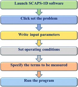 | ||
| Fig. 1 Schematic of the working approach of the SCAPS-1D simulator.23 | ||
The first three pilot equations are solved using the Newton–Raphson differentiation methods and Gummel-type iteration to calculate the quasi-Fermi levels and electrostatic potential of free carriers throughout the semiconductor. The electric field, carrier concentration, and other device potential parameters are then determined. Accurate selection of parameters for each layer of the PVSCs is crucial as the accuracy of the performance parameters depends on them. All physical parameters used in this simulation for each layer of the suggested Pt/N-doped Cu2O/MoTe2/ZnO/ITO/Al PVSCs are listed in Table 2. The data derived from the optical properties of MoTe2, ZnO, N-doped Cu2O, and ITO layers are taken from the existing literature for this simulation.17,42–45
| Parameters | ITO46 | ZnO35 | MoTe2![[thin space (1/6-em)]](https://www.rsc.org/images/entities/char_2009.gif) 23 23 |
N-doped Cu2O17 |
|---|---|---|---|---|
| Thickness, (μm) | 0.050 | 0.100 | 1.250 | 0.100 |
| Band-gap, Eg (eV) | 3.60 | 3.20 | 1.10 | 2.60 |
| Electron affinity, χ (eV) | 4.50 | 4.00 | 4.20 | 3.20 |
| Dielectric constant, εr | 8.90 | 9.00 | 13.0 | 6.60 |
| Effective DOS at conduction band density, Nc (cm−3) | 2.20 × 10¹⁸ | 4.00 × 10¹⁸ | 4.00 × 10¹⁶ | 2.50 × 10²⁰ |
| Effective DOS at valence band density, Nv (cm−3) | 1.80 × 10¹⁹ | 2.00 × 10¹⁹ | 3.00 × 10¹⁸ | 2.50 × 10²⁰ |
| Electron thermal velocity, (cm s−1) | 1.00 × 10⁷ | 1.00 × 10⁷ | 1.00 × 10⁷ | 1.00 × 10⁷ |
| Hole thermal velocity, (cm s−1) | 1.00 × 10⁷ | 1.00 × 10⁷ | 1.00 × 10⁷ | 1.00 × 10⁷ |
| Electron carrier mobility, μn (cm2 V−1 S−1) | 50.00 | 100.0 | 110.0 | 0.10 |
| Hole carrier mobility, μp (cm2 V−1 S−1) | 10.00 | 25.00 | 426.0 | 10.00 |
| Donor concentration, ND (cm−3) | 1.00 × 10²¹ | 1.00 × 10¹⁶ | 0.00 | 0.00 |
| Acceptor concentration, NA (cm−3) | 1.00 × 10⁷ | 0.00 | 1.00 × 10¹⁵ | 1.00 × 10¹⁹ |
| Defect density, Nt (cm−3) | 1.00 × 10¹⁴ | 1.00 × 10¹⁴ | 1.00 × 10¹³ | 1.00 × 10¹⁵ |
| Parameters | MoTe2/ZnO | N-doped Cu2O/MoTe2 |
|---|---|---|
| Types of defect | Neutral | Neutral |
| Capture cross section of electrons (cm2) | 1.00 × 10¹⁹ | 1.00 × 10¹⁹ |
| Capture cross section of holes (cm2) | 1.00 × 10¹⁹ | 1.00 × 10¹⁹ |
| Energetic distribution | 0.60 | 0.60 |
The device structure, as illustrated in Fig. 2(a), includes zinc oxide (ZnO) as a window layer, N-doped copper oxide (N-doped Cu2O) as a BSF layer, an ITO layer, and aluminum (Al) and platinum (Pt) as the front and back metal electrodes, respectively. The energy band structure of the proposed Pt/N-doped Cu2O/MoTe2/ZnO/ITO/Al PVSCs is portrayed in Fig. 2(b).
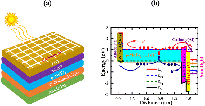 | ||
| Fig. 2 Design of the Pt/N-doped Cu2O/MoTe2/ZnO/ITO/Al PVSC (a) schematic blocks and (b) simulated energy band diagram. | ||
3. Results and discussion
3.1 Performance optimization of the MoTe2-based solar cell
 | (6) |
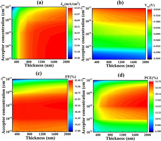
In Fig. 3(b), it is shown that increasing the doping concentration in a 1500 nm thick MoTe2 layer from 1013 cm−3 to 1017 cm−3 results in the VOC rising from 0.4 V to 0.794 V. This rise could be attributed to the shift in the quasi-Fermi energy level of holes as the acceptor concentration (NA) increases, or due to the heightened potential at the ZnO/MoTe2 junction, which is a consequence of a more robust depletion layer at higher doping densities, thereby improving charge separation and cell efficiency.17
In Fig. 3(c), the FF is observed to increase with the MoTe2 layer thickness at 1500 nm and the acceptor level rising from 1013 cm−3 to 1015 cm−3, climbing from 68.39% to 82.33%. This enhancement is linked to the reduced series resistance of the MoTe2 layer as the doping density increases.50 Nevertheless, a further increment in doping concentration from 1015 cm−3 to 1017 cm−3 causes a sharp decline in the FF value from 82.33% to 41.62%, indicating that too high a doping concentration may destabilize the system, leading to a rise in resistance and a fall in FF.
The influence of VOC, JSC, and FF on the PCE of the ZnO/MoTe2 device is depicted in the contour diagram of Fig. 3(d). According to Fig. 3(d), at a doping concentration of 1015 cm−3, there is an exponential increase in performance up to a thickness of 1500 nm, after which it plateaus. The observed result stems from the enhancement of photocurrent as the thickness increases; however, recombination may also increase in a thicker absorber layer due to the longer carrier transit time. Furthermore, Fig. 3(d) illustrates that the combined effects of VOC, JSC, and FF enhance the PCE up to a doping density of 1015 cm−3, beyond which the PCE begins to decline. The peak PCE of 24.75% was achieved with a MoTe2 layer thickness and doping concentration of 1500 nm and 1015 cm−3, respectively.
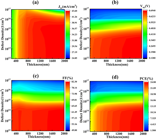
The defect density within the MoTe2 layer is a critical parameter that significantly impacts the device's performance. Fig. 4 presents contour plots of essential PV parameters against the thickness and defect density of the MoTe2 layer. As shown in Fig. 4(a), the JSC increases with thickness until a certain defect density of 1016 cm−3 is reached, beyond which it significantly decreases. Fig. 4(b)–(d) demonstrate that VOC and FF maintain PCE stability with thickness and up to a defect density of 1014 cm−3. However, larger defects cause a systematic decline in PCE across all thicknesses. Notably, at a MoTe2 layer thickness of 1500 nm, the VOC drops from 0.69 V to 0.52 V, and the FF decreases from 81.90% to 50.11% as the defect density increases from 1014 cm−3 to 1017 cm−3. This performance degradation results in a substantial efficiency drop, from 24.44% to 2.33%, as the defect density increases from 1014 cm−3 to 1017 cm−3, owing to Shockley–Read–Hall (SRH) recombination and the resulting rise in reverse saturation current.51,52 Thus, a thickness of 1250 nm, a carrier concentration of 1015 cm−3, and a defect density of 1014 cm−3 are identified as the optimal parameters for the MoTe2 absorber layer for the proposed device structure.
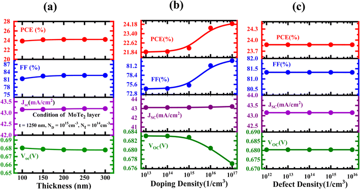 | ||
| Fig. 5 Variation of MoTe2/ZnO-based PVSC performance on the (a) thickness, (b) donor concentration, and (c) bulk defect density of the ZnO window layer. | ||
Fig. 5(b) demonstrates the change in VOC, JSC, FF, and PCE based on the doping concentration of the ZnO window layer, ranging from 1013 to 1017 cm−3. It is evident from Fig. 5(b) that the donor density does not affect JSC, while a slight decrement in VOC from 0.683 to 0.677 V is observed as the doping density increases. This originates from the coulomb traps due to high donor concentrations, which decrease electron mobility.53 Moreover, the FF significantly increases from 73 to 84% with the enhanced conductivity of the ZnO window layer due to the increase in doping density.54 The combined effect of VOC, JSC, and FF leads to an increase in PCE up to a particular doping density of 1016 cm−3, which then tends to saturate.
The impact of a rise in defects of the ZnO layer ranging from 1012 to 1016 cm−3 is illustrated in Fig. 5(c). As shown in Fig. 5(c), the performance parameters remain relatively unchanged across this range of defect densities in the ZnO layer. This suggests that the performance of the MoTe2/ZnO-based PVSC is not significantly affected by bulk defects in the ZnO layer. Consequently, a ZnO layer with a thickness of 100 nm, carrier concentration of 1016 cm−3, and bulk defect density of 1014 cm−3 is deemed optimal. Conversely, for the MoTe2 layer, a defect density of 1013 cm−3, doping concentration of 1015 cm−3, and thickness of 1250 nm are identified as the optimal performance conditions for further use.
3.2 MoTe2/ZnO-based PVSC performance dependent on the N-doped Cu2O as a back surface field (BSF) layer
Recombination at the device's rear side significantly hampers the PV performance of solar cells.17 The Back Surface Field (BSF) layer plays a vital role in solar cell design by enhancing the VOC and overall device performance. This section explores the significance of the BSF layer, detailing its function and impact on solar cell characteristics. The BSF layer's primary role is to minimize electron–hole pair recombination at the back contact, a process that leads to energy loss and reduced efficiency. Typically, the BSF layer is formed by doping the semiconductor material with a specific dopant. In p-type semiconductors like MoTe2, a heavily doped layer acts as the BSF, creating an electric field at the interface that repels minority carriers, leading to a higher VOC.A BSF with a high carrier density (p+) is implemented at the back side of the device to reduce surface recombination and enhance performance. N-doped Cu2O is employed as the BSF layer to capitalize on its potential. The energy band structure of the Al/ITO/ZnO/MoTe2/N-doped Cu2O/Pt PVSC under sunlight illumination is depicted in Fig. 2, and the properties of the N-doped Cu2O layer are detailed in Table 2. A minimal conduction band offset (CBO) of approximately 0.06 eV is observed at the conduction band edge between the MoTe2 and ZnO layers, while a significant CBO of about 1.5 eV is present between the absorber and BSF layers. Consequently, electrons generated by sunlight in the conduction band are reflected by the large CBO at the N-doped Cu2O band edge, facilitating smooth transport across the ZnO/MoTe2 interface due to the small CBO, leading to efficient collection of photo-electrons at the front electrode. Conversely, holes generated in the valence band of the absorber layer are impeded by the ZnO layer and reflected back due to a valence band offset (VBO) of approximately 2.04 eV between ZnO/MoTe2, allowing for their efficient extraction by the N-doped Cu2O layer and transport to the back-electrode, as the VBO between the MoTe2 and N-doped Cu2O layer is insignificantly low.
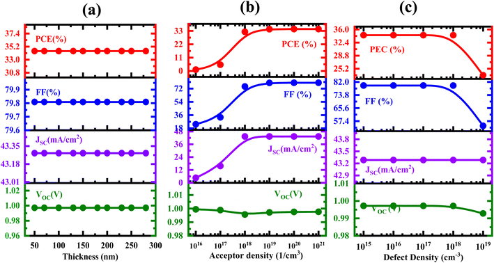 | ||
| Fig. 6 Dependency of MoTe2/ZnO-based PVSC performance on the (a) thickness, (b) donor concentration, and (c) bulk defect density of the N-doped Cu2O BSF layer. | ||
Fig. 6(b) illustrates the change in key performance parameters of the MoTe2/ZnO PVSC with the carrier density of the N-doped Cu2O BSF layer ranging from 1016 cm−3 to 1021 cm−3. Except for VOC, all the key parameters gradually increased with an increase in the carrier density from 1016 cm−3 to 1018 cm−3, above which the values remained constant in the current density range of 1018 cm−3 to 1021 cm−3. These results suggest that the sufficient electric field due to the BSF layer at the N-doped Cu2O/MoTe2 interface might be attained after a certain carrier concentration of 1018 cm−3.
The effect of increasing the defect density of the N-doped Cu2O BSF layer on the key performance parameters is shown in Fig. 6(c). As shown in Fig. 6(c), the performance parameters remain relatively unchanged up to the defect density of 1018 cm−3 in the N-doped Cu2O BSF layer. For a large amount of defect density of 1019 cm−3, the VOC and FF, resulting in PCE, sharply declined from 34.45% to 23.87% due to Shockley–Read–Hall (SRH) recombination. Consequently, an N-doped Cu2O BSF layer with a thickness of 100 nm, carrier concentration of 1019 cm−3, and bulk defect density of 1015 cm−3 is considered optimal.
 | (7) |
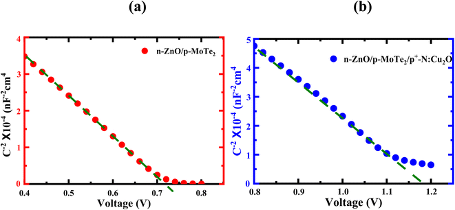 | ||
| Fig. 7 C–V analysis to evaluate the built-in potential of (a) ZnO/MoTe2 and (b) ZnO/MoTe2/N-doped Cu2O heterostructures. | ||
The linear section in Fig. 7(a), after fitting and extrapolation, reveals that the built-in potential (φbi) for the ZnO/MoTe2 device is approximately 0.72 V. However, the built-in potential for the ZnO/MoTe2/N-doped Cu2O device is determined to be 1.18 V. It is suggested that the cumulative effect of the ZnO/MoTe2 junction and MoTe2/N-doped Cu2O interface is responsible for improving the device's built-in potential, thereby aiding in the efficient separation of photo-induced carriers. The enhanced electric field created by the BSF layer promotes the drift of minority carriers towards the front contact, where they can contribute to the photocurrent. This results in a slightly improved JSC in the device. Additionally, due to the higher CB edge of the N-doped Cu2O compared to the MoTe2 edge, electrons generated in the absorber layer are repelled at the BSF layer's CB edge. This repulsion mitigates surface recombination at the rare interface, leading to a significantly higher VOC of the ZnO/MoTe2/N-doped Cu2O device. In other words, introducing a properly designed Back Surface Field (BSF) layer on the backside of the device generates an additional electric field at the BSF/Absorber (p+/p) interface.60 This electric field causes the reflection of minority carriers (electrons) approaching the BSF/Absorber (p+/p) interface. As a result, the recombination velocity, which refers to the number of carrier recombination per unit area and time, will decrease due to the presence of the electric field produced by the BSF layer. This reduction in recombination leads to an improvement in the open-circuit voltage (VOC) of the device.
 | (8) |
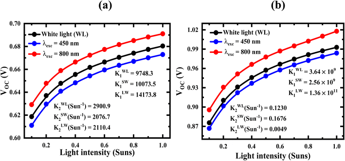
An intensity-dependent VOC analysis under monochromatic short and long wavelengths has been conducted to extract the recombination coefficient at the absorber/BSF interface (Ri,b0) and the surface recombination velocity (SRV) of electrons at the absorber/BSF interface. The study uses two monochromatic wavelengths, 450 nm and 800 nm, to illuminate the designed SCs for qualitative and quantitative assessments of recombination at the back interface without and with the BSF layer. Fig. 8 shows the VOC graphs dependent on light intensity (Ga) without and with the BSF layer. The K1 and K2 values, obtained from fitting the intensity-dependent VOC curves in Fig. 8 using eqn (8), are used to calculate the recombination coefficients Rd0, Ri,b0, and hence the recombination rates Rd, Ri,b as well as the surface recombination velocity of electrons at the back interface, which are presented in Table 3. Details of calculations of the recombination coefficient and surface recombination velocity are discussed in ES1.†
Table 3 reveals that the recombination coefficient and rate in the depletion region and at the back interface, along with the SRV at the back interface for ZnO/MoTe2, are notably poor. However, by integrating an N-doped Cu2O layer (100 nm) with ZnO/MoTe2, forming a ZnO/MoTe2/N-doped Cu2O structure, a significant reduction in the recombination coefficient in the depletion region and at the back interface, from 1.1 × 108 cm−2 s−1 to 7.1 × 106 cm−2 s−1 and 1.6 × 103 cm−2 s−1 to 1.3 × 10⁻³, respectively, is observed. Consequently, the recombination rate in the depletion region and at the back interface is suppressed from 2.77 × 1016 cm−2 s−1 to 1.75 × 10¹⁵ and 3.98 × 1011 cm−2 s−1 to 3.35 × 10⁵, respectively. Additionally, the SRV at the back interface is decreased from 200 cm s−1 to 1.69 × 10⁻³ cm s−1 by adding the N-doped Cu2O BSF layer. These findings imply that the electric field at the MoTe2/N-doped Cu2O interface enhances hole transport at the valence band from the MoTe2 absorber layer to the back contact via the N-doped Cu2O-BSF layer, mitigating the flow of minority carriers (electrons) towards the MoTe2/N-doped Cu2O junction at the conduction band, thus reducing the carrier recombination rate at the device's rear side, suppressing the dark current (J0). It is confirmed from eqn (6) that the open circuit voltage of the MoTe2-based PVSC in the presence of N-doped Cu2O is improved due to the suppression of the dark current.
| Condition | KSW1 | KLW1 | KWL1 | KSW2 | KLW2 | KWL2 | Rd0 (cm−2 s−1) | Ri,b0 (cm−2 s−1) | Rd (cm−2 s−1) | Ri,b (cm−2 s−1) | Sbe (cm s−1) |
|---|---|---|---|---|---|---|---|---|---|---|---|
| Without N-doped Cu2O-BSF layer | 10![[thin space (1/6-em)]](https://www.rsc.org/images/entities/char_2009.gif) 073 073 |
14![[thin space (1/6-em)]](https://www.rsc.org/images/entities/char_2009.gif) 173.8 173.8 |
9748.3 | 2076.7 | 2110.4 | 2901 | 1.1 × 10⁸ | 1.6 × 10³ | 2.77 × 10¹⁶ | 3.98 × 10¹¹ | 200 |
| with N-doped Cu2O-BSF layer | 2.56 × 10⁹ | 1.36 × 10¹¹ | 3.64 × 10⁹ | 0.1676 | 0.0049 | 0.123 | 7.1 × 10⁶ | 1.3 × 10⁻³ | 1.75 × 10¹⁵ | 3.35 × 10⁵ | 1.69 × 10⁻³ |
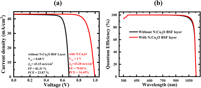 | ||
| Fig. 9 (a) Light-dependent output characteristic and (b) quantum efficiency curves for the proposed MoTe2/ZnO PVSC in the presence and absence of an N-doped Cu2O-BSF layer. | ||
Fig. 9(b) compares the quantum efficiency (QE) curves for both structures in the presence and absence of the N-doped Cu2O BSF layer. Simulations spanning a wavelength range of 300 nm to 1200 nm under AM1.5 solar illumination indicate similar QE curves for both cases. It is evident that the MoTe2/ZnO PVSC, in the presence and absence of the N-doped Cu2O BSF layer, exhibits nearly identical QE curves, indicating the N-doped Cu2O BSF layer does not contribute to photon absorption. However, it aids in enhancing the built-in potential by the additional N-doped Cu2O/MoTe2 junction, reducing recombination losses at the back side of the device to increase the VOC, leading to improved photovoltaic efficiency (Fig. 8).
3.3 Effect of metal work function at the back contact and operation temperature on the N-doped Cu2O/MoTe2/ZnO PVSC
In Fig. 10(a), the graph shows the normalized PV response for the back-contact metal work function ranging from 5.1 eV to 5.7 eV. This is to understand the behavior at the interface of the back-contact/BSF layer, whether it is ohmic or rectifying. The carrier concentration, thickness, and bulk defect of each layer have been kept at the optimized values obtained previously from the simulation. From Fig. 10(a), it can be observed that all the PV parameters except for JSC linearly increase with the increasing anode's work function up to a certain value of 5.32 eV. Beyond this value, further improvement in the metal work function of the back electrode shows diminishing returns. It is also noted in Fig. 10(a) that a Schottky-type rectifying behavior is observed at the N-doped Cu2O/anode interface for work functions less than 5.32 eV. This leads to the recombination of carriers at the back-contact/BSF interface, resulting in reduced VOC, FF, and consequently, photovoltaic efficiency, as shown in Fig. 10(a). It is well known that the energy barrier (φB) between the back surface anode metal and N-doped Cu2O-BSF layer can be evaluated by:
 | (9) |
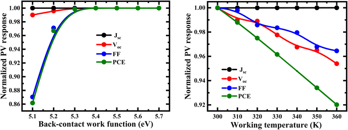 | ||
| Fig. 10 Key performance parameter responses of the N-doped Cu2O/MoTe2/ZnO PVSC in relation to (a) work function of the back-contact metal and (b) operating temperature. | ||
Conventionally, solar cells are typically designed to operate within a temperature range of 288 to 323 K when placed in the open air.67 The operating temperature is a critical factor as it greatly affects the PV response of the cells.68 Fig. 10(b) displays the effect of operating temperature on the optimized N-doped Cu2O/MoTe2/ZnO PVSC. It is noticed from Fig. 10(b) that a linear decrement of the VOC and FF leads to a decrease in PCE as the working temperature increases. This observation suggests that at higher temperatures, electrons acquire sufficient energy to recombine with holes before leaving the depletion zone.69 The temperature coefficient CT (% K−1) of PCE is a key parameter for PV devices to assess their stability, indicating how elevated operating temperatures impact the device's PCE, and can be expressed under standard test conditions (STC: 298 K) as follows:60
 | (10) |
 is extracted from the slope by fitting the PCE curve in Fig. 10(b). Now, using eqn (10), the temperature coefficient of PCE of the cell is evaluated to be −0.133% K−1, which is less than that of traditional Si (−0.5% K−1) and CIGS (−0.443% K−1) solar cells.23,70
3.4 Bifacial nature of the ZnO/MoTe2/N-doped Cu2O solar cell
The bifacial device is a strong candidate for improving energy harvesting capabilities per unit area to replace mono-facial solar cells without increasing cost and manufacturing complexity. Two independent simulations for back and front side illuminations of 1 sun are considered. The term bifacial factor (BF) is carried out to understand the asymmetric photoelectric behavior of bifacial devices. The relative feedback of each side can be realized by the BF, which is estimated by the following equation.
 | (11) |
Fig. 11 shows the J–V curves of an optimized N-doped Cu2O/MoTe2/ZnO solar cell under both front and back illumination at 1 sun. The PV performance slightly declines with back illumination at 1 sun, suggesting minor absorption losses at the device's rear surface. The bifacial factor (BF) for VOC and FF is calculated to be 99.49% and 99.89%, respectively, indicating negligible additional losses impacting VOC and FF under backside illumination. The BF for JSC is approximately 98.4%, reflecting a slight reduction in JSC due to absorption losses at the solar cell's back surface. Lastly, a BF for PCE of 97.6% is reported, corroborating earlier studies.17,71
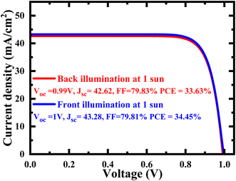 | ||
| Fig. 11 J–V curves of the optimized N-doped Cu2O/MoTe2/ZnO PVSC under back-illumination at 1 sun and front illumination at 1 sun for a bifacial PVSC. | ||
4. Conclusion and recommendations
Despite the inherent advantages of MoTe2, developing high-efficiency MoTe2-based solar cells faces a crucial challenge: achieving a high open-circuit voltage (VOC). The VOC is a key performance parameter that directly influences the overall efficiency of a solar cell. A high VOC is essential for maximizing the power output and achieving competitive efficiencies. This study examines the obstacles related to attaining a high VOC in MoTe2 thin film solar cells. It examines the pivotal role of the Back Surface Field (BSF) layer in enhancing VOC and introduces a novel bi-facial ZnO/MoTe2 solar cell with an N-doped Cu2O BSF layer. Our methodology relies on extensive device simulations utilizing the SCAPS-1D software to offer insights into the electrical properties and performance of the proposed device architecture. This study numerically investigated the potential of a bi-facial ZnO/MoTe2 solar cell with an N-doped Cu2O BSF layer for achieving high VOC. The incorporation of the N-doped Cu2O BSF layer effectively suppressed carrier recombination at the back contact, leading to a significant enhancement in VOC. The proposed device structure demonstrated a considerable increase in VOC compared to conventional designs, potentially enabling higher power conversion efficiency. The simulation results highlighted the importance of optimizing the thickness and doping concentration of the BSF layer to maximize its effectiveness. This research provides valuable insights into the design and optimization of MoTe2-based solar cells. Future research efforts should focus on:Experimental validation: conducting experimental fabrication and characterization of the proposed device structure to validate the simulation results.
Optimization of BSF layer: investigating different materials and deposition techniques for the BSF layer to further enhance its performance.
Integration with other technologies: exploring the integration of the bi-facial design with other advanced technologies, such as tandem solar cells or flexible substrates.
By addressing these recommendations, the development of high-performance MoTe2 solar cells with improved JSC and power conversion efficiency can be significantly accelerated, contributing to the advancement of renewable energy technologies.
Data availability
The data that support the findings of this study are available from the corresponding authors upon reasonable request.Conflicts of interest
The authors declare that there is no conflicts of interest in this work.Acknowledgements
This study was supported in part by the research centre, Bangabandhu Sheikh Mujibur Rahman Science and Technology University (BSMRSTU), Bangladesh.References
- M. T. Rizi, M. H. S. Abadi and M. Ghaneii, Two dimensional modeling of Cu2O heterojunction solar cells based-on β-Ga2O3 buffer, Optik, 2018, 155, 121–132 CrossRef.
- Z. Shi and A. H. Jayatissa, One-pot hydrothermal synthesis and fabrication of kesterite Cu2ZnSn(S,Se)4 thin films, Prog. Nat. Sci.:Mater. Int., 2017, 27, 550–555 CrossRef CAS.
- S. A. Vanalakar, P. S. Patil and J. H. Kim, Recent advances in synthesis of Cu2FeSnS4 materials for solar cell applications: a review, Sol. Energy Mater. Sol. Cells, 2018, 182, 204–219 CrossRef CAS.
- J. Li, D. Wang, X. Li, Y. Zeng and Y. Zhang, Cation substitution in earth-abundant kesterite photovoltaic materials, Adv. Sci., 2018, 5, 1700744 CrossRef PubMed.
- O. A. M. Abdelraouf and N. K. Allam, Nanostructuring for enhanced absorption and carrier collection in CZTS-based solar cells: coupled optical and electrical modeling, Opt. Mater., 2016, 54, 84–88 CrossRef CAS.
- R. W. Fessenden, J. Sobhanadri and V. Subramanian, Minority carrier lifetime in thin films of Zn,P, using microwave and optical transient measurements, Thin Solid Films, 1995, 266, 176–181 CrossRef CAS.
- G. Sai Gautam, T. P. Senftle and E. A. Carter, Understanding the effects of Cd and Ag doping in Cu2 ZnSnS4 solar cells, Chem. Mater., 2018, 30, 4543–4555 CrossRef CAS.
- K. Branker, M. J. M. Pathak and J. M. Pearce, A review of solar photovoltaic levelized cost of electricity, Renewable Sustainable Energy Rev., 2011, 15, 4470–4482 CrossRef.
- W. Ma, J. M. Luther, H. Zheng, Y. Wu and A. P. Alivisatos, Photovoltaic Devices Employing Ternary PbSxSe1-x Nanocrystals, Nano Lett., 2009, 9, 1699–1703 CrossRef CAS PubMed.
- W. Ma, S. L. Swisher, T. Ewers, J. Engel, V. E. Ferry, H. A. Atwater and A. P. Alivisatos, Photovoltaic Performance of Ultrasmall PbSe Quantum Dots, ACS Nano, 2011, 5, 8140–8147 CrossRef CAS PubMed.
- S. McDonald, G. Konstantatos, S. Zhang, P. Cyr, E. Klem, L. Levina and E. Sargent, Solution-Processed PbS Quantum Dot Infrared Photodetectors and Photovoltaics, Nat. Mater., 2005, 4, 138–144 CrossRef CAS PubMed.
- Z. Ning, D. Zhitomirsky, V. Adinolfi, B. Sutherland, J. Xu, O. Voznyy, P. Maraghechi, X. Lan, S. Hoogland, Y. Ren and E. H. Sargent, Graded Doping for Enhanced Colloidal Quantum Dot Photovoltaics, Adv. Mater., 2013, 25, 1719–1723 CrossRef CAS PubMed.
- W. Zhao, R. M. Ribeiro, M. Toh, A. Carvalho, C. Kloc, A. H. C. Neto and G. Eda, Origin of Indirect Optical Transitions in Few-Layer MoS2, WS2, and WSe2, Nano Lett., 2013, 13, 5627–5634 CrossRef CAS PubMed.
- S. Dominguez-Meister, A. Justo and J. Sanchez-Lopez, Synthesis and tribological properties of WSex films prepared by magnetron sputtering, Mater. Chem. Phys., 2013, 142, 186–194 CrossRef CAS.
- C. Chiritescu, D. G. Cahill, N. Nguyen, D. Johnson, A. Bodapati, P. Keblinski and P. Zschack, Ultralow Thermal Conductivity in Disordered, Layered WSe2 Crystals, Science, 2007, 315, 351–353 CrossRef CAS PubMed.
- S. T. Finn and J. E. Macdonald, Contact and Support Considerations in the Hydrogen Evolution Reaction Activity of Petaled MoS2 Electrodes, ACS Appl. Mater. Interfaces, 2016, 8, 25185–25192 CrossRef CAS PubMed.
- M. A. Rahman, Performance analysis of WSe2-based bifacial solar cells with different electron transport and hole transport materials by SCAPS-1D, Heliyon, 2022, 8, e09800 CrossRef PubMed.
- J. Liu, Y. Wang, X. Xiao, K. Zhang, N. Guo, Y. Jia, S. Zhou, Y. Wu, Q. Li and L. Xiao, Conversion of Multi-layered MoTe2 Transistor Between P-Type and N-Type and Their Use in Inverter, Nanoscale Res. Lett., 2018, 13(291), 1–9 Search PubMed.
- N. Rahman, M. D. Haque, M. F. Rahman, M. M. Islam, M. A. N. Juthi, A. R. Roy, M. A. Akter and M. F. Islam, Assessing the performance of MoTe2 based solar cell with Cu2O hole transport layer through device simulation, Discover Mater., 2023, 3(25), 1–7 Search PubMed.
- C. Gong, H. Li, H. Wang, C. Zhang, Q. Zhuang, A. Wang, Z. Xu, W. Cai, R. Li, X. Li and Z. Zang, Silver coordination-induced n-doping of PCBM for stable and efficient inverted perovskite solar cells, Nat. Commun., 2024, 15, 4922 CrossRef CAS PubMed.
- K. Wang, Z. Xu, Z. Guo, H. Wang, S. M. H. Qaid, K. Yang and Z. Zang, Phosphonate Diacid Molecule Induced Crystallization Manipulation and Defect Passivation for High-Performance Inverted MA-Free Perovskite Solar Cells, Adv. Energy Mater., 2024, 14, 2402249 CrossRef CAS.
- C. Zhang, H. Li, C. Gong, Q. Zhuang, J. Chen and Z. Zang, Crystallization manipulation and holistic defect passivation toward stable and efficient inverted perovskite solar cells, Energy Environ. Sci., 2023, 16, 3825–3836 RSC.
- A. Rajib, M. A. A. Kafi, M. M. H. Najesh, M. R. Hasan, M. R. Miah and A. Rahman, Performance analysis of 2D-MoTe2/2D-MoSe2 -based bifacial solar cells with N-doped Cu2O as BSF Layer by SCAPS-1D, Phys. Scr., 2024, 99, 055541 CrossRef CAS.
- A. Rajib, A. Kuddus, K. Yokoyama, T. Shida, K. Ueno and H. Shirai, Mist chemical vapor deposition of Al1-xTixOy thin films and their application to a high dielectric material, J. Appl. Phys., 2022, 131, 105301 CrossRef CAS.
- A. Rajib, A. Kuddus, T. Shida, K. Ueno and H. Shirai, Mist Chemical Vapor Deposition of AlOx Thin Films Monitored by a Scanning Mobility Particle Analyzer and its Application to the Gate Insulating Layer of Field-effect Transistors, ACS Appl. Electron. Mater., 2021, 3(2), 658–667 CrossRef CAS.
- A. Kuddus, A. Rajib, K. Yokoyama, T. Shida, K. Ueno and H. Shirai, Mist Chemical Vapor Deposition of Crystalline MoS2 Atomic Layer Films for Field-Effect Transistors, Nanotechnology, 2021, 33(4), 045601 CrossRef PubMed.
- B. Sultana, A. T. M. Islam, Md. Haque, A. Kuddus, Md. Ali and F. Rahman, Numerical study of MoSe2 -based dual-heterojunction with In2Te3 BSF layer toward high-efficiency photovoltaics, Phys. Scr., 2023, 98, 095935 CrossRef CAS.
- D. Puotinen and R. E. Newnham, The crystal structure of MoTe2, Acta Crystallogr., 1961, 14, 691–692 CrossRef CAS.
- R. R. Reeber, Lattice parameters of ZnO from 4.20 to 296 0K, J. Appl. Phys., 1970, 41, 5063–5066 CrossRef CAS.
- Y. Wang, J. Ghanbaja, D. Horwat, L. Yu and J. F. Pierson, Nitrogen chemical state in N-doped Cu2O thin films, Appl. Phys. Lett., 2017, 110, 131902 CrossRef.
- I. Alam, R. Mollick and Md. A. Ashraf, Numerical simulation of Cs2AgBiBr6-based perovskite solar cell with ZnO nanorod and P3HT as the charge transport layers, Phys. B, 2021, 618, 413187 CrossRef CAS.
- S. S. A. Askari, M. Kumar and M. K. Das, Numerical study on the interface properties of a ZnO/c-Si heterojunction solar cell, Semicond. Sci. Technol., 2018, 33, 115003 CrossRef.
- N. Dinh Lam, Modelling and numerical analysis of ZnO/CuO/Cu2O heterojunction solar cell using SCAPS, Eng. Res. Express, 2020, 2, 025033 CrossRef.
- M. Manoua, T. Jannane, K. El-Hami and L. Ahmed, Investigation of n-ZnO/p-GaAs Heterojunction Solar Cell Using Two-Dimensional Numerical Simulation, Recent Adv. Photonics Optoelectron., 2023, 75, 3601–3611 CAS.
- B. Mozafari and A. Shahhoseini, Using Molybdenum Trioxide as a TCO Layer to Improve Performance of CdTe/CdS1 Thin-film Solar Cell, Signal Process. Renew. Energy, 2020, 4(3), 57–65 Search PubMed.
- D. Parajuli, K. C. Devendra, K. B. Khattri, D. R. Adhikari, R. A. Gaib and D. K. Shah, Numerical assessment of optoelectrical properties of ZnSe–CdSe solar cell-based with ZnO antireflection coating layer, Sci. Rep., 2023, 13, 12193 CrossRef CAS PubMed.
- Y. A. Wahmane, H. Mouhib, B. Ydir, A. A. Hssi, L. Atourki, A. Ihlal and K. Bouabid, Comparison study between ZnO and TiO2 in CuO based solar cell using SCAPS-1D, Mater. Today Proc., 2022, 52, 166–171 CrossRef.
- M. Gholipoor, N. Solhtalab and M. H. Mohammadi, High-performance parallel tandem MoTe2/perovskite solar cell based on reduced graphene oxide as hole transport layer, Sci. Rep., 2022, 12, 20455 CrossRef CAS PubMed.
- I. Kriegel, J. Rodriguez-Fernandez, E. Da Como, A. A. Lutich, J. M. Szeifert and J. Feldmann, Tuning the Light Absorption of Cu1.97S Nanocrystals in Supercrystal Structures, Chem. Mater., 2011, 23, 1830–1834 CrossRef CAS.
- M. Burgelman, J. Verschraegen, S. Degrave and P. Nollet, Modeling thin-film PV devices, Prog. Photovoltaics, 2004, 12(2–3), 143–153 CAS.
- M. Burgelman, P. Nollet and S. Degrave, Modelling polycrystalline semiconductor solar cells, Thin Solid Films, 2000, 361, 527–532 CrossRef.
- F. Liu, J. Zhu, J. Wei, Y. Li, M. Lv, S. Yang, B. Zhang, J. Yao and S. Dai, Numerical simulation: Toward the design of high-efficiency planar perovskite solar cells, Appl. Phys. Lett., 2014, 104, 253508 CrossRef.
- K. Wu, H. Ma, Y. Gao and J. Yang, Highly-efficient heterojunction solar cells based on two-dimensional tellurene and transition metal dichalcogenides, J. Mater. Chem. A, 2019, 7, 7430–7436 RSC.
- B. K. Mondal, S. K. Mostaque and J. Hossain, Unraveling the effects of a GeSe BSF layer on the performance of a CuInSe2 TFSCs: a computational analysis, Opt. Continuum, 2023, 2, 428–440 CrossRef CAS.
- A. Bedia, F. Z. Bedia, M. Aillerie and B. Benyoucef, Morphological and Optical Properties of ZnO Thin Films Prepared by Spray Pyrolysis on Glass Substrates at Various Temperatures for Integration in Solar Cell, Energy Procedia, 2015, 74, 529–538 CrossRef CAS.
- J. Hossain, M. Rahman, M. M. A. Moon, B. K. Mondal, M. F. Rahman and M. H. K. Rubel, Guidelines for a highly efficient CuI/n-Si heterojunction solar cell, Eng. Res. Express, 2020, 2, 045019 CrossRef.
- S. M. Sze and K. K. Ng, LEDs and lasers, Phys. Semicond. Devices, 2006, 3, 601–657 Search PubMed.
- M. D. Wanda, S. Ouédraogo, F. Tchoff, F. Zougmoré and J. M. B. Ndjaka, Numerical Investigations and Analysis of Cu2ZnSnS4 Based Solar Cells by SCAPS-1D, Int. J. Photoenergy, 2016, 1–9 CrossRef.
- B. H. Patel and S. S. Patel, Growth and electrical properties of flash evaporated AgGaTe2 thin films, Cryst. Res. Technol., 2006, 41(2), 117–122 CrossRef CAS.
- A. Rana, A. Kumar, M. W. Rahman, N. Vashistha, K. K. Garg, S. Pandey and R. K. Singh, Non-approximated series resistance evaluation by considering high ideality factor in organic solar cell, AIP Adv., 2018, 8, 125121 CrossRef.
- N. F. Mott, Metal-insulator transition, Rev. Mod. Phys., 1968, 40(4), 677 CrossRef CAS.
- S. Rai, B. K. Pandey and D. K. Dwivedi, Modeling of highly efficient and low cost CH3NH3Pb (I1-xClx)3 based perovskite solar cell by numerical simulation, Opt. Mater., 2020, 100, 109631 CrossRef CAS.
- A. Ghosh, S. S. Dipta, S. S. S. Nikor, N. Saqib and A. Saha, Performance analysis of an efficient and stable perovskite solar cell and a comparative study of incorporating metal oxide transport layers, J. Opt. Soc. Am. B, 2020, 37(7), 1966 CrossRef CAS.
- S. Ahmmed, A. Aktar, M. F. Rahman, J. Hossain and A. B. M. Ismail, A numerical simulation of high efficiency CdS/CdTe based solar cell using NiO HTL and ZnO TCO, Optik, 2020, 223, 165625 CrossRef CAS.
- S. Sze and N. Kwok, Physics of Semiconductor Devices, Wiley-Interscience, 3rd edn, 2007 Search PubMed.
- S. M. Sze, C. R. Crowell and D. Kahng, Current transport in metal-semiconductor barriers, J. Appl. Phys., 1964, 35, 2534 CrossRef.
- A. T. M. Islam, M. E. Karim, A. Rajib, Y. Nasuno, T. Ukai, S. Kurosu, M. Tokuda, Y. Fujii, Y. Nakajima, T. Hanajiri and H. Shirai, Chemical mist deposition of organic for efficient front- and back-PEDOT:PSS/crystalline Si heterojunction solar cells, Appl. Phys. Lett., 2019, 114, 193901 CrossRef.
- A. Rajib, K. M. Enamul, S. Kurosu, T. Ukai, M. Tokuda, Y. Fujii, T. Hanajiri, R. Ishikawa, K. Ueno and H. Shirai, Synthesis of AlOx thin films by atmospheric-pressure mist chemical vapor deposition for surface passivation and electrical insulator layers, J. Vac. Sci. Technol., A, 2020, 38, 033413 CrossRef CAS.
- M. J. Nayeen, B. K. Mondal, S. R. Basu and J. Hossain, Theoretical exploration of high VOC in Cu2SnS3 TFSCss towards high efficiency, Sol. Energy, 2023, 265, 112076 CrossRef CAS.
- A. Rahman M, Design and simulation of a high-performance Cd-free Cu2SnSe3 solar cells with SnS electron-blocking hole transport layer and TiO2 electron transport layer by SCAPS-1D, SN Appl. Sci., 2021, 3(2), 253 CrossRef.
- S. Paul, S. Grover, I. L. Repins, B. M. Keyes, M. A. Contreras, K. Ramanathan, R. N. Z. Zhao, F. Liao and J. V. Li, Analysis of Back-Contact Interface Recombination in Thin-Film Solar Cells, IEEE J. Photovoltaics, 2018, 8(3), 871–878 Search PubMed.
- M. A. Rahman, Numerical modeling of ultra-thin CuSbS2 heterojunction solar cell with TiO2 electron transport and CuAlO2:Mg BSF layers, Opt. Mater. Express, 2022, 12(8), 2954–2972 CrossRef CAS.
- S. Demtsu and J. Sites, Effect of back-contact barrier on thin-film CdTe solar cells, Thin Solid Films, 2006, 510(1–2), 320–324 CrossRef CAS.
- B. Ofuonye, J. Lee, M. Yan, C. Sun, J. M. Zuo and I. Adesida, Electrical and microstructural properties of thermally annealed Ni/Au and Ni/Pt/Au Schottky contacts on AlGaN/GaN heterostructures, Semicond. Sci. Technol., 2014, 29, 095005 CrossRef CAS.
- D. Zhaobin, F. Wu, Y. C. Wang and H. Jiang, Hong, Theoretical studies of the work functions of Pd-based bimetallic surfaces, J. Chem. Phys., 2015, 142, 214706 CrossRef PubMed.
- D. Etor, M. Ekele and I. Akintunde, Impact of Metal Work-Function on Current Rectification by Metal-Insulator-Metal Diodes, J. Eng. Technol., 2022, 7(2), 430–434 Search PubMed.
- S. Sze and K. K. Ng, Physics of Semiconductor Devices, John Wiley and Sons, Inc., 1981 Search PubMed.
- P. Singh and N. Ravindra, Temperature dependence of solar cell performance-an analysis, Sol. Energy Mater. Sol. Cells, 2012, 101, 36–45 CrossRef CAS.
- J. Li, H. Wang, M. Luo, J. Tang, C. Chen, W. Liu, F. Liu, Y. Sun, J. Hand and Y. Zhang, 10% Efficiency Cu2ZnSn(S,Se)4 TFSCss fabricated by magnetron sputtering with enlarged depletion region width, Sol. Energy Mater. Sol. Cells, 2016, 149, 242–249 CrossRef CAS.
- M. Fathi, M. Abderrezek, F. Djahli and M. Ayad, Study of TFSCss in high temperature condition, Energy Procedia, 2015, 74, 1410–1417 CrossRef CAS.
- A. B. Phillips, K. K. Subedi, G. K. Liyanage, F. K. Alfadhili, R. J. Ellingson and M. J. Heben, Understanding and advancing bifacial TFSCss, ACS Appl. Energy Mater., 2020, 3, 6072–6078 CrossRef CAS.
Footnote |
| † Electronic supplementary information (ESI) available: Measurement procedures for recombination coefficient and surface recombination velocity details are available upon request. See DOI: https://doi.org/10.1039/d4ra05974c |
| This journal is © The Royal Society of Chemistry 2024 |

