 Open Access Article
Creative Commons Attribution 3.0 Unported Licence
Analysis of dislocation defects in compositionally step-graded α-(AlxGa1−x)2O3 layers
Tatsuya Yasuokaa,
Hiromu Susamia,
Li Liu ab,
Giang T. Dangab and
Toshiyuki Kawaharamura*ab
aSchool of Systems Engineering, Kochi University of Technology, 185 Miyanokuchi, Tosayamada, Kami, Kochi, 782-8502, Japan
bCenter for Nanotechnology, Research Institute, Kochi University of Technology, 185 Miyanokuchi, Tosayamada, Kami, Kochi 782-8502, Japan. E-mail: kawaharamura.toshiyuki@kochi-tech.ac.jp
First published on 4th October 2024
Abstract
The ultra-wide bandgap semiconductor α-Ga2O3 can be heteroepitaxially grown on a sapphire substrate. However, due to a lattice mismatch of about 4.6% with a sapphire substrate, many dislocation defects occur in α-Ga2O3 films. To reduce the dislocation density, compositionally step-graded α-(AlxGa1−x)2O3 layers were fabricated on a c-plane sapphire substrate using mist CVD. TEM measurements revealed few dislocations in the initial layer of α-(Al0.96Ga0.04)2O3, but numerous dislocations were observed in the subsequent layer of α-(Al0.84Ga0.16)2O3. However, the step-graded α-(AlxGa1−x)2O3 layers exhibited bending of the dislocations under both compressive and tensile strains due to compositional differences of α-(AlxGa1−x)2O3, resulting in about 50% reduction of the dislocation density in the high-Ga-composition layer of α-(AlxGa1−x)2O3. The introduction of multiple 50 nm α-Ga2O3 layers into the compositionally step-graded α-(AlxGa1−x)2O3 layers resulted in a notable reduction in dislocation defects at the interface between the sandwiched α-Ga2O3 layers. It is assumed that the dislocations were bent by the strain caused by the composition change, resulting in a decrease in the number of dislocations. It is anticipated that further reduction of dislocation density will be achieved by optimizing the composition change and thicknesses of layers that provide effective strain for dislocation bending, and by stacking these layers.
1. Introduction
Gallium oxide (Ga2O3) is gaining attention as an ultra-wide bandgap semiconductor material. Ga2O3 has various crystal structures,1 and among them, the thermally most stable phase is β-Ga2O3 with a band gap of ∼4.9 eV,2,3 which can be grown from melt.4–7 Thus, homoepitaxial growth is possible,8–10 and β-Ga2O3 has been the most actively studied. On the other hand, α-Ga2O3, which has a corundum structure and is thermally metastable, has the largest band gap of 5.3 eV (ref. 11) (5.61 eV),12 among Ga2O3 polymorphs of different crystal structures and can be heteroepitaxially grown on a sapphire substrate.11,13–18 It can be mixed with other corundum-structured oxides α-(MxGa1−x)2O3 [M = Al,19–24 In,25 Fe,26 Cr,27 and Ir28] to control various properties such as band gaps and lattice constants, and is expected to be used for power devices. However, the sapphire substrate and α-Ga2O3 have about 4.60% lattice mismatch along the a-axis,29 and many dislocations are formed due to this large lattice mismatch.30,31 This high dislocation density is one of the most significant problems to be solved in α-Ga2O3 device applications. Previous studies have examined the Epitaxial Lateral Overgrowth (ELO) method32–35 and the introduction of α-(AlxGa1−x)2O3 buffer layers20,36,37 to decrease dislocation density. In this study, we have attempted to fabricate compositionally step-graded α-(AlxGa1−x)2O3 layers to reduce the dislocation density. Additionally, in a previous study, the dislocation density was reduced with the introduction of quasi-graded α-(AlxGa1−x)2O3 buffer layers, although the mechanism behind it was unclear.36 This study revealed the mechanism by analyzing dislocations in the step-graded α-(AlxGa1−x)2O3 layers.2. Experimental details
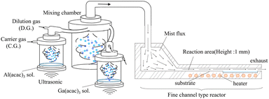
To fabricate compositionally step-graded α-(AlxGa1−x)2O3 layers, it is necessary to determine the growth rate for each α-(AlxGa1−x)2O3 composition. Therefore, several α-(AlxGa1−x)2O3 thin films with different compositions were grown and their growth rates were investigated. The growth conditions are summarized in Table 1. Gallium(III) acetylacetonate (Ga(acac)3) and aluminum(III) acetylacetonate (Al(acac)3) were used as precursors for Ga and Al, respectively. They were dissolved in a mixture of deionized water and hydrochloric acid (HCl) at concentrations of 20 mM and 40 mM, respectively. A schematic diagram of the mist CVD system used for α-(AlxGa1−x)2O3 growth in this work is shown in Fig. 1. Mist generated by the ultrasonic transducers from each solution chamber was well mixed in a dedicated mixing chamber and then supplied to a fine channel reactor. Details of this mist CVD system were described in ref. 38–42. Nitrogen was used as carrier and dilution gases, and α-(AlxGa1−x)2O3 thin films of different compositions were grown by changing the ratio of Al/Ga carrier gas flow rates. Dilution gas flows were adjusted accordingly to maintain a total flow rate of 6.0 L min−1 for each solution chamber, resulting in a total flow rate of 12 L min−1 in the reactor. α-(AlxGa1−x)2O3 thin films were grown on c-plane sapphire substrates at 450 °C.| Solution | A | B |
|---|---|---|
| a Gallium acetylacetonate, 99.99%, Sigma-Aldrich.b Aluminum acetylacetonate, 99.99%, Sigma-Aldrich.c De-ionized water, Merck Millipore.d Hydrochloric acid, 35–37%, Wako Pure Chemical Corporation. | ||
| Solute | Ga(acac)3a | Al(acac)3b |
| Concentration | 20 mM | 40 mM |
| Solvent (mixing ratio) | DI waterc![[thin space (1/6-em)]](https://www.rsc.org/images/entities/char_2009.gif) : :![[thin space (1/6-em)]](https://www.rsc.org/images/entities/char_2009.gif) HCld (199 HCld (199![[thin space (1/6-em)]](https://www.rsc.org/images/entities/char_2009.gif) : :![[thin space (1/6-em)]](https://www.rsc.org/images/entities/char_2009.gif) 1) 1) |
|
| Gas | N2 | |
| Substrate | c-Plane sapphire | |
| Growth temperature | 450 °C | |
| Growth system | 3G mist CVD | |
| Ultrasonic transducer | 2.4 MHz, 24 V–0.625 A (×3) | |
3. Results and discussion
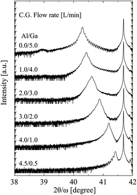
The XRD spectra are shown in Fig. 2. The peaks in the range of 40.3–41.7° correspond α-(AlxGa1−x)2O3 (0006), and the peak at around 38.9° corresponds to ε-Ga2O3 (004). The origin of the peak at 41.9° remains unidentified. The peak corresponding to α-(AlxGa1−x)2O3 (0006) shifted towards the high-angle side as the carrier gas ratio of Al increased, suggesting that the composition of α-(AlxGa1−x)2O3 could be readily controlled. The α-(AlxGa1−x)2O3 composition ratio in the film was determined by analyzing the peak positions, as Vegard's law applies to α-(AlxGa1−x)2O3.19 Additionally, the thickness of each α-(AlxGa1−x)2O3 film was determined by the fringe spacing. The summarized dependencies of composition ratios and growth rates on carrier gas ratios are shown in Fig. 3. Although the thickness of the α-(AlxGa1−x)2O3 film, which was grown using a carrier gas ratio of Al/Ga = 2.0/3.0 L min−1, could not be calculated due to unclear fringes, it was found that the growth rate can be approximated linearly with the Al/Ga carrier gas ratio under the present growth conditions.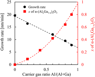 | ||
| Fig. 3 Dependences of growth rates and composition ratios x of α-(AlxGa1−x)2O3 on carrier gas ratio Al/(Al + Ga). | ||
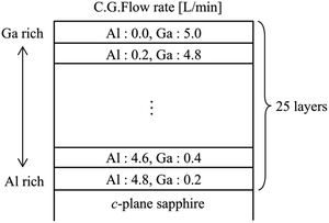
Next, Fig. 4 shows the schematic diagram of the fabricated compositionally step-graded α-(AlxGa1−x)2O3 layers. The Al carrier gas was decreased by 0.2 L min−1 from 4.8 to 0.0 L min−1, and the Ga carrier gas was increased by 0.2 L min−1 from 0.2 to 5.0 L min−1, so that the composition gradually changed from α-Al2O3 to α-Ga2O3, forming a total of 25 layers. Table 2 summarizes the carrier gas flow rates and actual film thicknesses of all layers. The thicknesses were equal to or thicker than 50 nm and the growth times were determined based on the results in Fig. 3. α-(AlxGa1−x)2O3 layers with high Al compositions were thicker than 50 nm due to the presence of compressive strains observed in the high-Al compositions, whereas other layers were 50 nm thick. To grow this structure, the Al and Ga precursor solutions used were the same as those listed in Table 1. Prior to the growth, the c-plane sapphire substrate was immersed in a 5![[thin space (1/6-em)]](https://www.rsc.org/images/entities/char_2009.gif) :
:![[thin space (1/6-em)]](https://www.rsc.org/images/entities/char_2009.gif) 2 solution of sulfuric acid and hydrogen peroxide for 10 minutes, followed by a further rinse in deionized water for at least 10 minutes.
2 solution of sulfuric acid and hydrogen peroxide for 10 minutes, followed by a further rinse in deionized water for at least 10 minutes.
| Layer | Thickness (nm) | Carrier gas flow rate | |
|---|---|---|---|
| Al (L min−1) | Ga (L min−1) | ||
| 1 | 80 | 4.8 | 0.2 |
| 2 | 75 | 4.6 | 0.4 |
| 3 | 70 | 4.4 | 0.6 |
| 4 | 65 | 4.2 | 0.8 |
| 5 | 60 | 4.0 | 1.0 |
| 6 | 58 | 3.8 | 1.2 |
| 7 | 56 | 3.6 | 1.4 |
| 8 | 54 | 3.4 | 1.6 |
| 9 | 52 | 3.2 | 1.8 |
| 10 | 50 | 3.0 | 2.0 |
![[thin space (1/6-em)]](https://www.rsc.org/images/entities/char_2009.gif) |
|||
| 50 | Decrease by 0.2 | Increase by 0.2 | |
| 25 | 50 | 0.0 | 5.0 |
Fig. 5 shows reciprocal space mapping around the (10![[1 with combining macron]](https://www.rsc.org/images/entities/char_0031_0304.gif) ,10) reflection and the dashed line in the figure connects the ideal peak positions of α-Al2O3 (qx: 0.243, qz: 0.770) and α-Ga2O3 (qx: 0.232, qz: 0.744).43 The peak near the reflection from the sapphire substrate did not follow the dashed line, indicating that high-Al-composition layers seem to have been subjected to a slight in-plane compressive strain. This suggests that a large lattice mismatch occurred between the layer under compressive strain and the relaxed layer. In contrast, in other regions, peaks were observed along the dashed line, indicating that α-(AlxGa1−x)2O3 layers were fully relaxed.
,10) reflection and the dashed line in the figure connects the ideal peak positions of α-Al2O3 (qx: 0.243, qz: 0.770) and α-Ga2O3 (qx: 0.232, qz: 0.744).43 The peak near the reflection from the sapphire substrate did not follow the dashed line, indicating that high-Al-composition layers seem to have been subjected to a slight in-plane compressive strain. This suggests that a large lattice mismatch occurred between the layer under compressive strain and the relaxed layer. In contrast, in other regions, peaks were observed along the dashed line, indicating that α-(AlxGa1−x)2O3 layers were fully relaxed.
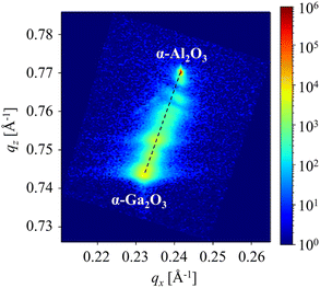 | ||
Fig. 5 Reciprocal space mapping around (10![[1 with combining macron]](https://www.rsc.org/images/entities/char_0031_0304.gif) ,10) reflections from compositionally step-graded α-(AlxGa1−x)2O3 layers. ,10) reflections from compositionally step-graded α-(AlxGa1−x)2O3 layers. | ||
Fig. 6(a) shows a cross-sectional high-angle annular dark-field scanning transmission electron microscopy (HAADF-STEM) image of the sample thinned to 100 nm thickness. The formation of the 1st to 16th, 24th, and 25th layers could be seen in the order from the sapphire substrate. In addition, voids or low-density regions were observed in the 2nd and 3rd layers. Fig. 6(b) and (c) show energy dispersive X-ray (EDX) and cross-sectional bright-field STEM (BF-STEM) images, respectively. Few dislocations were observed in the 1st layer, but the occurrence of many dislocations was observed starting from the 2nd layer. The dislocation density was estimated to be 7.5 × 1010 cm−2 in the high-Al-composition region using the Ham method.44 The EDX analysis reveals that the first and second layers were α-(Al0.96Ga0.04)2O3 and α-(Al0.84Ga0.16)2O3, with a lattice mismatch of about 0.57% along the a-axis. Although this lattice mismatch value is smaller than that between α-Al2O3 and α-Ga2O3 (about 4.60%), the dislocation density is comparable to that of α-Ga2O3 grown directly on a sapphire substrate.30 This indicates that more smoothly compositionally graded layers may be needed or that it might be hard to drastically reduce dislocation density by compositionally step-graded α-(AlxGa1−x)2O3 layers. On the other hand, it was also found that the dislocations were bent and reduced due to being dislocated out of the TEM sample or pair annihilation in the compositionally graded α-(AlxGa1−x)2O3. The dislocation density in the high-Ga-composition region was determined to be 3.6 × 1010 cm−2, which is approximately half of that in the high-Al-composition region, and is similar to the results reported by B. Kim et al.37 This indicates that the dislocation can be completely bent in the in-plane direction to eliminate the dislocations in the crystal growing on it, or even if not completely bent, the bending can induce pair annihilation, resulting in a reduction in the dislocation density. Based on the EDX results, the x of α-(AlxGa1−x)2O3 decreased gradually from the substrate interface. However, there were three areas where it increased and the dislocation bending, dislocation disappearance from the TEM specimen, or pair annihilation occurred in the vicinity of these areas [Fig. 6(b) and (c)]. This indicates that the dislocation can be bent by compositional changes, suggesting that the use of a superlattice buffer, which alternates compressive and tensile strain by changing the composition of the α-(AlxGa1−x)2O3, may be effective in reducing the dislocation density.
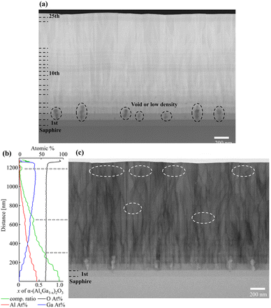 | ||
| Fig. 6 Cross-sectional (a) HAADF-STEM and (c) BF-STEM images, and (b) EDX spectra of compositionally step-graded α-(AlxGa1−x)2O3 layers. | ||
To elucidate the mechanism of dislocation reduction by strained superlattice buffer layers, structures were fabricated with α-Ga2O3 inserted in the compositionally step-graded α-(AlxGa1−x)2O3 buffer layers. Table 3 shows the fabrication conditions. The fabrication conditions for the compositionally step-graded α-(AlxGa1−x)2O3 layers were identical to those described in Table 2, except for the introduction of four α-Ga2O3 layers of 50 nm thickness within the aforementioned step-graded α-(AlxGa1−x)2O3 layers.
| Layer | Thickness (nm) | Carrier gas flow rate | |
|---|---|---|---|
| Al (L min−1) | Ga (L min−1) | ||
| 1 | 80 | 4.8 | 0.2 |
| 2 | 75 | 4.6 | 0.4 |
| 3 | 70 | 4.4 | 0.6 |
| 4 | 65 | 4.2 | 0.8 |
| 5 | 60 | 4.0 | 1.0 |
| 6 | 50 | 0.0 | 5.0 |
| 7 | 58 | 3.8 | 1.2 |
| 8 | 56 | 3.6 | 1.4 |
| 9 | 54 | 3.4 | 1.6 |
| 10 | 52 | 3.2 | 1.8 |
| 11 | 50 | 3.0 | 2.0 |
| 12 | 50 | 0.0 | 5.0 |
| 13 | 50 | 2.8 | 2.2 |
![[thin space (1/6-em)]](https://www.rsc.org/images/entities/char_2009.gif) |
|||
| 50 | Decrease by 0.2 | Increase by 0.2 | |
| 17 | 50 | 2.0 | 3.0 |
| 18 | 50 | 0.0 | 5.0 |
| 19 | 50 | 1.8 | 3.2 |
| 23 | 50 | 1.0 | 4.0 |
| 24 | 50 | 0.0 | 5.0 |
| 25 | 50 | 0.8 | 4.2 |
| 29 | 500 | 0.0 | 5.0 |
Fig. 7 illustrates the reciprocal space mapping around the (10![[1 with combining macron]](https://www.rsc.org/images/entities/char_0031_0304.gif) ,10) reflection of the sample that was fabricated in accordance with the fabrication condition in Table 3. As in Fig. 5, the ideal peak positions of α-Al2O3 and α-Ga2O3 are connected by dashed lines. In Fig. 5, the sample exhibited a slight compressive strain in the high-Al-composition region. However, in Fig. 7, it follows the dashed line and was fully relaxed. Conversely, as the Ga composition increased, the α-(AlxGa1−x)2O3 peak was observed to be situated above and to the left of the dashed line, indicating that it was subjected to tensile strain. Furthermore, the α-Ga2O3 peak extended to the lower right side, indicating that it was subjected to compressive strain. The insertion of α-Ga2O3 in the compositionally step-graded α-(AlxGa1−x)2O3 layers resulted in the complete relaxation of the α-(AlxGa1−x)2O3 layers in proximity to the substrate interface. However, the remaining α-(AlxGa1−x)2O3 layers were subjected to tensile strain, and the α-Ga2O3 layers between the α-(AlxGa1−x)2O3 layers experienced compressive strain.
,10) reflection of the sample that was fabricated in accordance with the fabrication condition in Table 3. As in Fig. 5, the ideal peak positions of α-Al2O3 and α-Ga2O3 are connected by dashed lines. In Fig. 5, the sample exhibited a slight compressive strain in the high-Al-composition region. However, in Fig. 7, it follows the dashed line and was fully relaxed. Conversely, as the Ga composition increased, the α-(AlxGa1−x)2O3 peak was observed to be situated above and to the left of the dashed line, indicating that it was subjected to tensile strain. Furthermore, the α-Ga2O3 peak extended to the lower right side, indicating that it was subjected to compressive strain. The insertion of α-Ga2O3 in the compositionally step-graded α-(AlxGa1−x)2O3 layers resulted in the complete relaxation of the α-(AlxGa1−x)2O3 layers in proximity to the substrate interface. However, the remaining α-(AlxGa1−x)2O3 layers were subjected to tensile strain, and the α-Ga2O3 layers between the α-(AlxGa1−x)2O3 layers experienced compressive strain.
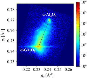 | ||
Fig. 7 Reciprocal space mapping around (10![[1 with combining macron]](https://www.rsc.org/images/entities/char_0031_0304.gif) ,10) reflections from compositionally step-graded α-(AlxGa1−x)2O3 layers with insertions of α-Ga2O3 layers. ,10) reflections from compositionally step-graded α-(AlxGa1−x)2O3 layers with insertions of α-Ga2O3 layers. | ||
Fig. 8(a) and (b) show the results of the EDX analysis and the BF-STEM image respectively. As can be seen in Fig. 8(b), the formation of four α-Ga2O3 layers in the step-graded α-(AlxGa1−x)2O3 layers were confirmed. Region A revealed numerous dislocations were originated from the second layer and were consistent with the observations shown in Fig. 6(c). These findings suggest that up to α-(Al0.96Ga0.04)2O3 can be grown on the c-plane sapphire substrate without the presence of dislocations. In contrast, the formation of voids or low-density areas was observed to be more prevalent than in Fig. 6(c). The dislocation densities of regions A, B, C, D, and the surface α-Ga2O3 were estimated to be 6.56 × 1010 cm−2, 6.32 × 1010 cm−2, 5.85 × 1010 cm−2, 5.21 × 1010 cm−2, and 3.71 × 1010 cm−2 respectively. The reduction rates were −3.7% for regions A to B, −7.5% for B to C, −10.8% for C to D, and −28.9% for D to surface α-Ga2O3 respectively. It is assumed that the smaller compositional alterations were more readily strain without relaxation, resulting in a greater number of dislocations being bent and thus reducing the number of dislocations.
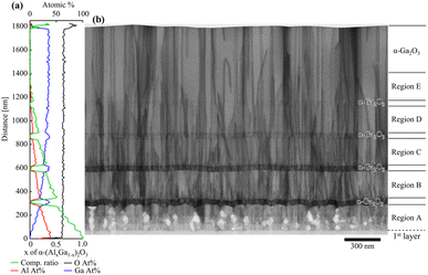 | ||
| Fig. 8 (a) EDX spectra and (b) cross-sectional BF-STEM image of compositionally step-graded α-(AlxGa1−x)2O3 layers with insertions of α-Ga2O3 layers. | ||
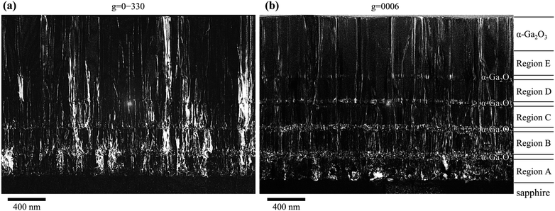
Fig. 9(a) and (b) show g/3g weak-beam dark-field (WB-DF) images acquired along 〈2![[1 with combining macron]](https://www.rsc.org/images/entities/char_0031_0304.gif)
![[1 with combining macron]](https://www.rsc.org/images/entities/char_0031_0304.gif) 0〉 zone axis with diffraction vectors g = 0–330 and g = 0006, respectively. In Fig. 9(a), the formation of numerous edge dislocations was confirmed at the interface with the substrate, originating from the second or third layer of step-graded α-(AlxGa1−x)2O3 layers. These dislocations exhibited a gradual decrease after the α-Ga2O3 layers grown between α-(AlxGa1−x)2O3 layers, particularly within regions D and E. In contrast, Fig. 9(b) shows that the formation of screw dislocations originated from the second layer of step graded α-(AlxGa1−x)2O3 layers. However, a comparison between regions A and B suggests more dislocations in Region B. Given that previous research has indicated that the number of screw dislocations in α-Ga2O3 grown directly on sapphire substrates was less than 107 cm−2,30 it can be postulated that the screw dislocations were formed by the insertion of α-Ga2O3 layers. However, the number of screw dislocations exhibited a decrease in regions C, D, and E, with the α-Ga2O3 layer serving as the separation point. In particular, a notable reduction in screw dislocations was observed between regions B and C. This indicates that when the thickness of the α-Ga2O3 layer sandwiched between the α-(AlxGa1−x)2O3 layers is 50 nm, it is effective to apply a smaller composition change, hence, a smaller strain to reduce edge dislocations and a larger composition change, hence, a larger strain to reduce screw dislocations. Although this study only varied the composition of α-(AlxGa1−x)2O3, it would be interesting to investigate how dislocations change when the film is strained by varying the thicknesses of each layer, as this also contributes to the strain. From Fig. 9(a) and (b), the edge dislocation density, screw dislocation density, and mixed dislocation density in the surface α-Ga2O3 layer were estimated to be 1.71 × 1010 cm−2, 5.20 × 109 cm−2, and 1.34 × 1010 cm−2 respectively. These values were comparable to those obtained in previous studies utilizing quasi-graded α-(AlxGa1−x)2O3 buffer layers.36 The quasi-graded buffer layer was composed of multiple layers of two distinct α-(AlxGa1−x)2O3 compositions, exhibiting varying thicknesses. In consideration of the findings of the present study, it can be posited that the dislocation density was decreased as a result of the effective strain for dislocation bending in specific layers of a given thickness. It is expected that further reduction of dislocation density will be achieved in future investigations by optimizing the film thickness and the compositional change of α-(AlxGa1−x)2O3 that applies effective strain to the dislocation bending, as well as by layering multiple layers of these films.
0〉 zone axis with diffraction vectors g = 0–330 and g = 0006, respectively. In Fig. 9(a), the formation of numerous edge dislocations was confirmed at the interface with the substrate, originating from the second or third layer of step-graded α-(AlxGa1−x)2O3 layers. These dislocations exhibited a gradual decrease after the α-Ga2O3 layers grown between α-(AlxGa1−x)2O3 layers, particularly within regions D and E. In contrast, Fig. 9(b) shows that the formation of screw dislocations originated from the second layer of step graded α-(AlxGa1−x)2O3 layers. However, a comparison between regions A and B suggests more dislocations in Region B. Given that previous research has indicated that the number of screw dislocations in α-Ga2O3 grown directly on sapphire substrates was less than 107 cm−2,30 it can be postulated that the screw dislocations were formed by the insertion of α-Ga2O3 layers. However, the number of screw dislocations exhibited a decrease in regions C, D, and E, with the α-Ga2O3 layer serving as the separation point. In particular, a notable reduction in screw dislocations was observed between regions B and C. This indicates that when the thickness of the α-Ga2O3 layer sandwiched between the α-(AlxGa1−x)2O3 layers is 50 nm, it is effective to apply a smaller composition change, hence, a smaller strain to reduce edge dislocations and a larger composition change, hence, a larger strain to reduce screw dislocations. Although this study only varied the composition of α-(AlxGa1−x)2O3, it would be interesting to investigate how dislocations change when the film is strained by varying the thicknesses of each layer, as this also contributes to the strain. From Fig. 9(a) and (b), the edge dislocation density, screw dislocation density, and mixed dislocation density in the surface α-Ga2O3 layer were estimated to be 1.71 × 1010 cm−2, 5.20 × 109 cm−2, and 1.34 × 1010 cm−2 respectively. These values were comparable to those obtained in previous studies utilizing quasi-graded α-(AlxGa1−x)2O3 buffer layers.36 The quasi-graded buffer layer was composed of multiple layers of two distinct α-(AlxGa1−x)2O3 compositions, exhibiting varying thicknesses. In consideration of the findings of the present study, it can be posited that the dislocation density was decreased as a result of the effective strain for dislocation bending in specific layers of a given thickness. It is expected that further reduction of dislocation density will be achieved in future investigations by optimizing the film thickness and the compositional change of α-(AlxGa1−x)2O3 that applies effective strain to the dislocation bending, as well as by layering multiple layers of these films.
4. Conclusions
In conclusion, compositionally step-graded α-(AlxGa1−x)2O3 layers were grown on a c-plane sapphire substrate using mist CVD. Few dislocations were observed in the initial α-(Al0.96Ga0.04)2O3 layer; however, numerous dislocations were confirmed from the subsequent α-(Al0.84Ga0.16)2O3 layer. The dislocation density was similar to that of α-Ga2O3 grown directly on sapphire substrates. However, the dislocation density in the high-Ga-composition α-(AlxGa1−x)2O3 layer was decreased by approximately 50% due to the dislocation bending in the α-(AlxGa1−x)2O3 layers. This dislocation bending was observed in the α-(AlxGa1−x)2O3 layers where alternating compressive and tensile stresses were applied as a result of composition differences. To clarify the mechanism of dislocation bending, compositionally step-graded α-(AlxGa1−x)2O3 layers inserted with several α-Ga2O3 layers was fabricated. The dislocations were reduced following the insertion of α-Ga2O3 layers into the compositionally step-graded α-(AlxGa1−x)2O3. The results of the reciprocal space mapping indicate that this α-Ga2O3 layer was strained, and it is proposed that the dislocations are bent by the strain caused by the compositional change of α-(AlxGa1−x)2O3, resulting in the reduction of dislocations. The differentiation of dislocation types according to the WB-DF images revealed that smaller strains resulting from smaller compositional changes were effective in reducing edge dislocations, whereas larger strains resulting from larger compositional changes were effective in reducing screw dislocations. It is expected that future investigations will achieve a further reduction in dislocation density by optimizing the film thickness and the compositional change of α-(AlxGa1−x)2O3, which applies effective strain to the dislocation bending. Additionally, the use of multiple layers of these films will be examined as a means of further reducing dislocation density.Data availability
The data supporting this article is included in the manuscript.Author contributions
Tatsuya Yasuoka – conceptualization, methodology, investigation, visualization, and writing original draft; Hiromu Susami – investigation; Li Liu – methodology and investigation; Giang T. Dang – methodology and writing review & editing; Toshiyuki Kawaharamura – conceptualization, project administration, supervision, methodology, and writing review & editing.Conflicts of interest
There are no conflicts to declare.References
- H. Y. Playford, A. C. Hannon, E. R. Barney and R. I. Walton, Chem.–Eur. J., 2013, 19, 2803 CrossRef CAS PubMed.
- M. Orita, H. Ohta, M. Hirano and H. Hosono, Appl. Phys. Lett., 2000, 77, 4166 CrossRef CAS.
- T. Onuma, S. Saito, K. Sasaki, T. Masui, T. Yamaguchi, T. Honda and M. Higashiwaki, Jpn. J. Appl. Phys., 2015, 54, 112601 CrossRef.
- A. B. Chase, J. Am. Ceram. Soc., 1964, 47, 470 CrossRef CAS.
- A. Kuramata, K. Koshi, S. Watanabe, Y. Yamaoka, T. Masui and S. Yamakoshi, J. Appl. Phys., 2016, 55, 1202A2 CrossRef.
- K. Hoshikawa, E. Ohba, T. Kobayashi, J. Yanagisawa, C. Miyagawa and Y. Nakamura, J. Cryst. Growth, 2016, 447, 36 CrossRef CAS.
- Z. Galazka, R. Uecker, D. Klimm, K. Irmscher, M. Naumann, M. Pietsch, A. Kwasniewski, R. Bertram, S. Ganschow and M. Bickermann, ECS J. Solid State Sci. Technol., 2017, 6(2), Q3007 CrossRef CAS.
- K. Sasaki, A. Kuramata, T. Masui, E. G. Víllora, K. Shimamura and S. Yamakoshi, Appl. Phys. Express, 2012, 5, 035502 CrossRef.
- G. Wagner, M. Baldini, D. Gogova, M. Schmidbauer, R. Schewski, M. Albrecht, Z. Galazka, D. Klimm and R. Fornari, Phys. Status Solidi A, 2014, 211(1), 27 CrossRef CAS.
- H. Murakami, K. Nomura, K. Goto, K. Sasaki, K. Kawara, Q. Tu Thieu, R. Togashi, Y. Kumagai, M. Higashiwaki, A. Kuramata, S. Yamakoshi, B. Monemar and A. Koukitu, Appl. Phys. Express, 2015, 8, 015503 CrossRef CAS.
- D. Shinohara and S. Fujita, Jpn. J. Appl. Phys., 2008, 47, 7311 CrossRef CAS.
- A. Segura, L. Artús, R. Cuscó, R. Goldhahn and M. Feneberg, Phys. Rev. Mater., 2017, 1, 024604 CrossRef.
- D. Shinohara, H. Nishinaka, T. Ohshima, K. Kiba, Y. Kamada, T. Kawaharamura, and S. Fujita, The 55th JSAP Spring Meeting, 28a-W-2, 2008 Search PubMed.
- T. Wakamatsu, H. Takane, K. Kaneko, T. Araki and K. Tanaka, Jpn. J. Appl. Phys., 2023, 62, SF1024 CrossRef CAS.
- Y. Oshima, E. G. Víllora and K. Shimamura, Appl. Phys. Express, 2015, 8, 055501 CrossRef.
- K. Goto, H. Nakahata, H. Murakami and Y. Kumagai, Appl. Phys. Lett., 2020, 117, 222101 CrossRef CAS.
- Z. Cheng, M. Hanke, P. Vogt, O. Bierwagen and A. Trampert, Appl. Phys. Lett., 2017, 111, 162104 CrossRef.
- A. F. M. A. U. Bhuiyan, Z. Feng, H. L. Huang, L. Meng, J. Hwang and H. Zhao, APL Mater., 2021, 9, 101109 CrossRef CAS.
- G. T. Dang, T. Yasuoka, Y. Tagashira, T. Tadokoro, W. Theiss and T. Kawaharamura, Appl. Phys. Lett., 2018, 113, 062102 CrossRef.
- G. T. Dang, S. Sato, Y. Tagashira, T. Yasuoka, L. Liu and T. Kawaharamura, APL Mater., 2020, 8, 101101 CrossRef CAS.
- R. Jinno, K. Kaneko and S. Fujita, Jpn. J. Appl. Phys., 2021, 60, SBBD13 CrossRef CAS.
- R. Jinno, C. S. Chang, T. Onuma, Y. Cho, S. T. Ho, D. Rowe, M. C. Cao, K. Lee, V. Protasenko, D. G. Schlom, D. A. Muller, H. G. Xing and D. Jena, Sci. Adv., 2021, 7(2), eabd5891 CrossRef CAS PubMed.
- T. Uchida, R. Jinno, S. Takemoto, K. Kaneko and S. Fujita, Jpn. J. Appl. Phys., 2018, 57, 040314 CrossRef.
- G. T. Dang, Y. Tagashira, T. Yasuoka, L. Liu and T. Kawaharamura, AIP Adv., 2020, 10, 115019 CrossRef CAS.
- N. Suzuki, K. Kaneko and S. Fujita, J. Cryst. Growth, 2014, 401, 670 CrossRef CAS.
- K. Kaneko, T. Nomura, I. Kakeya and S. Fujita, Appl. Phys. Express, 2009, 2, 075501 CrossRef.
- K. Kaneko, T. Nomura and S. Fujita, Phys. Status Solidi C, 2010, 7, 2467 CrossRef CAS.
- K. Kaneko, Y. Masuda, S. I. Kan, I. Takahashi, Y. Kato, T. Shinohe and S. Fujita, Appl. Phys. Lett., 2021, 118, 102104 CrossRef CAS.
- R. Schewski, G. Wagner, M. Baldini, D. Gogova, Z. Galazka, T. Schulz, T. Remmele, T. Markurt, H. Von Wenckstern, M. Grundmann, O. Bierwagen, P. Vogt and M. Albrecht, Appl. Phys. Express, 2015, 8, 011101 CrossRef CAS.
- K. Kaneko, H. Kawanowa, H. Ito and S. Fujita, Jpn. J. Appl. Phys., 2012, 51, 020201 CrossRef.
- T. C. Ma, X. H. Chen, Y. Kuang, L. Li, J. Li, F. Kremer, F. F. Ren, S. L. Gu, R. Zhang, Y. D. Zheng, H. H. Tan, C. Jagadish and J. D. Ye, Appl. Phys. Lett., 2019, 115, 182101 CrossRef.
- Y. Oshima, K. Kawara, T. Shinohe, T. Hitora, M. Kasu and S. Fujita, APL Mater., 2019, 7, 022503 CrossRef.
- G. T. Dang, T. Yasuoka and T. Kawaharamura, Appl. Phys. Lett., 2021, 119, 041902 CrossRef CAS.
- R. Jinno, N. Yoshimura, K. Kaneko and S. Fujita, Jpn. J. Appl. Phys., 2019, 58, 120912 CrossRef CAS.
- Y. Oshima, H. Ando and T. Shinohe, Appl. Phys. Express, 2023, 16, 065501 CrossRef.
- R. Jinno, T. Uchida, K. Kaneko and S. Fujita, Appl. Phys. Express, 2016, 9, 071101 CrossRef.
- B. Kim, D. Yang, W. Sohn, S. Lee, H. H. C. Choi, T. Jang, E. Yoon, Y. Park and H. W. Jang, Acta Mater., 2021, 221, 117423 CrossRef CAS.
- T. Kawaharamura, Jpn. J. Appl. Phys., 2014, 53, 05FF08 CrossRef.
- T. Kawaharamura, M. Nishi, L. Liu, P. Rutthongjan, Y. Ishikawa, M. Sakamoto, T. Yasuoka, K. Asako, T. Ozaki, M. Fukue, M. Ueda, S. Sato and G. T. Dang, Jpn. J. Appl. Phys., 2024, 63, 015502 CrossRef.
- L. Liu, T. Kawaharamura, G. T. Dang, E. K. C. Pradeep, S. Sato, T. Uchida, S. Fujita, T. Hiramatsu, H. Kobayashi and H. Orita, Jpn. J. Appl. Phys., 2019, 58, 025502 CrossRef CAS.
- P. Rutthongjan, M. Nishi, L. Liu, S. Sato, Y. Okada, G. T. Dang and T. Kawaharamura, Appl. Phys. Express, 2019, 12, 065505 CrossRef CAS.
- P. Rutthongjan, L. Liu, M. Nishi, M. Sakamoto, S. Sato, E. K. C. Pradeep, G. T. Dang and T. Kawaharamura, Jpn. J. Appl. Phys., 2019, 58, 035503 CrossRef CAS.
- M. Oda, K. Kaneko, S. Fujita and T. Hitora, Jpn. J. Appl. Phys., 2016, 55, 1202B4 CrossRef.
- R. K. Ham, Philos. Mag., 1961, 6, 1183 CrossRef.
| This journal is © The Royal Society of Chemistry 2024 |

