 Open Access Article
Effect of zinc and magnesium ion doping on leakage current behavior of Ba0.6Sr0.4TiO3 thin film
Hong-zhe Wang *a and
Bo Lib
aSchool of Electronic Information Engineering, Department of Electronic and Communication Engineering, Shanghai DianJi University, Shanghai, 201306, People's Republic of China. E-mail: wanghz@sdju.edu.cn
bSchool of Electronic Information Engineering, Department of Software Engineering, Shanghai DianJi University, Shanghai, 201306, People's Republic of China
First published on 7th October 2024
Abstract
We report an in-depth analysis of the carrier conduction mechanisms in multilayer doped Ba0.6Sr0.4TiO3 films, which offers a significant new message for reducing the leakage current. First, Ba0.6Sr0.4TiO3 (BST) sol, Ba0.6Sr0.4Ti0.99Zn0.01O3 (ZBST) sol, and Ba0.6Sr0.4Ti0.99Mg0.01O3 (MBST) sol were prepared using the sol–gel method. Then, BST, ZBST, MBST, and binary alternating-structure Ba0.6Sr0.4Ti0.99Zn0.01O3/Ba0.6Sr0.4Ti0.99Mg0.01O3/Ba0.6Sr0.4Ti0.99Zn0.01O3 (ZMZ) thin films were designed and prepared. The effects of single-component doping and binary alternating doping on the interface barrier height and trap barrier height of the Ba0.6Sr0.4TiO3 thin films were studied. The results showed that the interface barrier height of ZMZ thin films is 0.55 eV, and the interface barrier height of BST thin films is 0.53 eV. Compared with the ZBST and MBST thin films, the change in the interface barrier height of the ZMZ film was not obvious. The trap barrier height of the ZMZ thin film is 0.17 eV, and the trap potential barrier height of the BST thin film is 0.12 eV. The trap barrier heights of ZBST thin films and MBST thin films are 0.15 eV and 0.16 eV, respectively. The enhancement of the trap barrier height may be related to the weakening of the trap and donor effects caused by oxygen vacancy defects. The energy band diagram shows the relationship between the oxygen vacancy defects, interface barrier height, and trap barrier height.
1. Introduction
Theoretically, perovskite titanate films are used as insulators. In fact, there are some defects in the prepared films, and a leakage current problem always exists.1 Understanding the leakage current in perovskite titanate thin films is a fundamental problem in the current scientific field. In view of the application of titanate thin films in microwave/radiofrequency electronic devices, the leakage current of Ba1−xSrxTiO3 (BST)-based materials has been widely studied.2–5 Previous research has shown that the leakage current of BST-based films is mainly influenced by the conductance between the film and electrode interface (interfacial conductance) and the conductance of the films themselves.6,7 The conductance between the film and electrode interface is related to the transport of carriers at the interface, which is mainly manifested as electron conductance. The conductance of the film itself is related to the transport of carriers in the film, which manifests mainly as ionic conductance. In this regard, researchers have studied the leakage current characteristics of BST-based films and analyzed the related leakage current mechanism. In most cases, tunneling and Schottky–Simmons are the main forms of conductance at the film–electrode interface. The Poole–Frenkel emission and space charge limited current model (SCLC) are the main forms of self-conductance.8,9 To make BST-based thin films better suited to microwave/RF electronic devices, researchers have done a lot of work, such as doping donor impurities and acceptor impurities. The results show that the leakage current of BST-based films doped with major impurities is significantly improved.10–12 Some researchers believe that when acceptor impurities are introduced into BST-based films, charged defects formed in the films to maintain electrical neutrality are the main reason for the change in the leakage current.13 However, some researchers have attributed the change in leakage current to the change in the depletion layer width at the film interface.14,15 In addition, it has been reported that the reason for the decrease in leakage current density in BST-based films is related to the change in the barrier height.14,16,17 With the deepening of our understanding of this phenomenon, we clearly realized that acceptor impurities play an important role in reducing the leakage current density of BST-based films. However, in the existing literature, most research results on the leakage current behavior of BST-based films are focused on single-component doped BST-based films, and there are few reports on the leakage current behavior of binary alternately doped BST films, especially the change in barrier height in the films. Based on this, we focused on the change in barrier height of binary alternately doped BST films replaced by acceptor doping ions (Mg2+ and Zn2+) and preliminarily analyzed the mechanism related to the change in barrier height. BST films alternately doped with zinc and magnesium ions were prepared using the sol–gel method. The interface barrier height and trap barrier height of each film were obtained using the Richardson–Schottky and Poole–Frenkel emission models, respectively.2. Methods
All thin film samples were prepared on a Pt/Ti/SiO2/Si substrate using the sol–gel method, and they were labeled as BST, MBST, ZBST, and ZMZ, respectively. And the specific implementation process is as follows:(a) Barium acetate, strontium acetate and tetrabutyl titanate were weighed in turn according to the molar ratio of 6![[thin space (1/6-em)]](https://www.rsc.org/images/entities/char_2009.gif) :
:![[thin space (1/6-em)]](https://www.rsc.org/images/entities/char_2009.gif) 4
4![[thin space (1/6-em)]](https://www.rsc.org/images/entities/char_2009.gif) :
:![[thin space (1/6-em)]](https://www.rsc.org/images/entities/char_2009.gif) 10. Then, barium acetate and strontium acetate were dissolved in hot glacial acetic acid and stirred at 70 °C for 15–20 minutes to obtain barium–strontium precursor solution (A). Weighing a certain amount of ethylene glycol methyl ether according to the molar ratio of glacial acetic acid to ethylene glycol methyl ether of 2
10. Then, barium acetate and strontium acetate were dissolved in hot glacial acetic acid and stirred at 70 °C for 15–20 minutes to obtain barium–strontium precursor solution (A). Weighing a certain amount of ethylene glycol methyl ether according to the molar ratio of glacial acetic acid to ethylene glycol methyl ether of 2![[thin space (1/6-em)]](https://www.rsc.org/images/entities/char_2009.gif) :
:![[thin space (1/6-em)]](https://www.rsc.org/images/entities/char_2009.gif) 1, fully mixing it with tetrabutyl titanate, and stirring at room temperature for 15–20 minutes to obtain titanium source precursor solution (B). The precursor of barium–strontium titanate sol (Ba0.6Sr0.4TiO3) was obtained by fully mixing barium–strontium precursor solution (A) and titanium source precursor solution (B). Weigh a certain amount of polyvinylpyrrolidone (PVP) according to the molar ratio of 7
1, fully mixing it with tetrabutyl titanate, and stirring at room temperature for 15–20 minutes to obtain titanium source precursor solution (B). The precursor of barium–strontium titanate sol (Ba0.6Sr0.4TiO3) was obtained by fully mixing barium–strontium precursor solution (A) and titanium source precursor solution (B). Weigh a certain amount of polyvinylpyrrolidone (PVP) according to the molar ratio of 7![[thin space (1/6-em)]](https://www.rsc.org/images/entities/char_2009.gif) :
:![[thin space (1/6-em)]](https://www.rsc.org/images/entities/char_2009.gif) 1000 to tetrabutyl titanate, and add it into the precursor of barium–strontium titanate sol, and fully stir until it is completely dissolved. Subsequently, a certain amount of acetylacetone was weighed according to the molar ratio of glacial acetic acid to acetylacetone of 10
1000 to tetrabutyl titanate, and add it into the precursor of barium–strontium titanate sol, and fully stir until it is completely dissolved. Subsequently, a certain amount of acetylacetone was weighed according to the molar ratio of glacial acetic acid to acetylacetone of 10![[thin space (1/6-em)]](https://www.rsc.org/images/entities/char_2009.gif) :
:![[thin space (1/6-em)]](https://www.rsc.org/images/entities/char_2009.gif) 1, and added to the above mixed solution. Finally, the mixed solution was stirred for 5–7 hours in a constant temperature water bath at 65 °C, and cooled to room temperature, and finally barium–strontium titanate sol (Ba0.6Sr0.4TiO3) was obtained.
1, and added to the above mixed solution. Finally, the mixed solution was stirred for 5–7 hours in a constant temperature water bath at 65 °C, and cooled to room temperature, and finally barium–strontium titanate sol (Ba0.6Sr0.4TiO3) was obtained.
(b) Barium acetate, strontium acetate, tetrabutyl titanate and zinc acetate (magnesium acetate) were weighed in turn according to the molar ratio of 60![[thin space (1/6-em)]](https://www.rsc.org/images/entities/char_2009.gif) :
:![[thin space (1/6-em)]](https://www.rsc.org/images/entities/char_2009.gif) 40
40![[thin space (1/6-em)]](https://www.rsc.org/images/entities/char_2009.gif) :
:![[thin space (1/6-em)]](https://www.rsc.org/images/entities/char_2009.gif) 99
99![[thin space (1/6-em)]](https://www.rsc.org/images/entities/char_2009.gif) :
:![[thin space (1/6-em)]](https://www.rsc.org/images/entities/char_2009.gif) 1. Then, barium acetate, strontium acetate and zinc acetate (magnesium acetate) were dissolved in hot glacial acetic acid and stirred at 70 °C for 15–20 minutes to obtain zinc (magnesium)–barium–strontium precursor solution (C). The precursor solution (A) of titanium source and the precursor solution (C) of zinc (magnesium), barium–strontium titanate sol precursors (Ba0.6Sr0.4Ti0.99Zn0.01O3, Ba0.6Sr0.4Ti0.99Mg0.01O3) doped with zinc (magnesium) ions are obtained. Subsequently, polyvinylpyrrolidone and acetylacetone were added to the mixed solution in turn at intervals of 15 minutes, and they were stirred for 5–7 hours under the condition of constant temperature water bath at 65 °C, and cooled to room temperature to obtain zinc (magnesium) ion-doped barium–strontium titanate sol Ba0.6Sr0.4Ti0.99X0.01O3 (X: Zn or Mg).
1. Then, barium acetate, strontium acetate and zinc acetate (magnesium acetate) were dissolved in hot glacial acetic acid and stirred at 70 °C for 15–20 minutes to obtain zinc (magnesium)–barium–strontium precursor solution (C). The precursor solution (A) of titanium source and the precursor solution (C) of zinc (magnesium), barium–strontium titanate sol precursors (Ba0.6Sr0.4Ti0.99Zn0.01O3, Ba0.6Sr0.4Ti0.99Mg0.01O3) doped with zinc (magnesium) ions are obtained. Subsequently, polyvinylpyrrolidone and acetylacetone were added to the mixed solution in turn at intervals of 15 minutes, and they were stirred for 5–7 hours under the condition of constant temperature water bath at 65 °C, and cooled to room temperature to obtain zinc (magnesium) ion-doped barium–strontium titanate sol Ba0.6Sr0.4Ti0.99X0.01O3 (X: Zn or Mg).
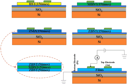
The structural design and testing principles of the thin films are illustrated in Fig. 1. All thin-film samples were spin-coated using spin-coating technology and a KW-4A desktop spin coater. Among them BST, MBST, and ZBST films were spin-coated for 12 s at a speed of 500 rpm and then spin-coated for 40 s at a speed of 4000 rpm (the same materials were deposited 15 times). However, for the ZBST/MBST/ZBST thin films, each layer was spin-coated for 12 s at a speed of 300 rpm, and then spin-coated for 40 s at a speed of 2000 rpm (the same material was deposited five times). Finally, the average thickness of all films was approximately 450 nm.
To better study the conduction mechanism related to the leakage current of each film, the current–voltage (J–E) characteristic curves of each film at different temperatures were measured using a semiconductor parameter analyzer. Before the test, a gold top electrode with a thickness of approximately 150 nm was deposited on all films using a small ion sputtering instrument (the size of the mask was 0.3 mm and the deposition time was 15 min). Subsequently, to avoid unnecessary influence on the leakage current test due to the deterioration of the film surface, all the films sputtered from the top electrode were heat-treated. Finally, the etching solution used to etch the edge of the bottom thin film was prepared to expose the thin film from the bottom electrode to form a gold top electrode-thin film-platinum bottom electrode structure. The volume ratio of the components of the etching solution was 1![[thin space (1/6-em)]](https://www.rsc.org/images/entities/char_2009.gif) :
:![[thin space (1/6-em)]](https://www.rsc.org/images/entities/char_2009.gif) 3
3![[thin space (1/6-em)]](https://www.rsc.org/images/entities/char_2009.gif) :
:![[thin space (1/6-em)]](https://www.rsc.org/images/entities/char_2009.gif) 10 (hydrofluoric acid, dilute nitric acid with a volume fraction of 60%, and deionized water).
10 (hydrofluoric acid, dilute nitric acid with a volume fraction of 60%, and deionized water).
3. Results and discussion
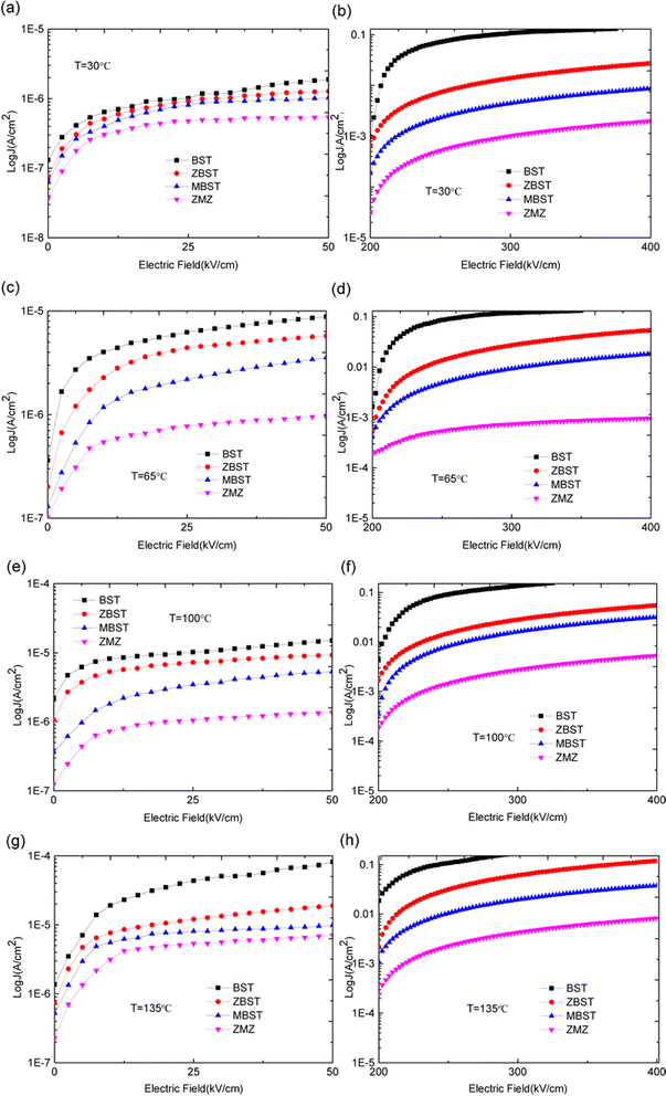
The experimental results for the crystallinity and micromorphology of each film are consistent with the results of our previous work.18 Therefore, the phase and micromorphology of each film are not presented herein. However, to study the change in barrier height in different doped films, we carried out the following experiments. First, the current–voltage (I–V) characteristic curves of the films at different temperatures were obtained and the conduction mechanism of carriers in the films was studied. Second, the barrier heights (interface barrier height and trap barrier height) were calculated according to the different conduction mechanisms. Finally, based on the experimental data, an energy band structure diagram is provided, which is convenient for analyzing the relationship between oxygen vacancy defects and barrier height.The J–E characteristic curves of the BST, MBST, ZBST, and ZMZ films at different temperatures and electric fields are shown in Fig. 2. In order to facilitate the observation and analysis of the relative growth rate of data, logarithmic scale is selected for the Y axis. It means for a given data point J, we can convert it into J′ by the formula: J′ = log10(J). The figure shows that the leakage current density of binary alternately doped thin films (ZMZ) is three orders of magnitude lower than that of undoped thin films (BST) and one order of magnitude lower than that of single ion-doped thin films (ZBST, MBST) under the condition of higher electric field; in other words, the leakage current of ZMZ thin films is the smallest, which is consistent with the results of XRD and SEM in previous work. The smaller the grain size, the more grain boundaries there are in the film. Therefore, whether the grain boundaries are regarded as series or parallel connection, ZMZ films have the largest resistance value, and the larger resistance value may be the reason why ZMZ films have the smallest leakage current density. Under a small electric field, there was no obvious difference in the leakage current density of all films in order of magnitude. In addition, the leakage current density of each film strongly depended on the temperature. That is, with an increase in temperature, the leakage current density of each film increases to different degrees, which may be related to the thermionic emission formed under thermal motion.19
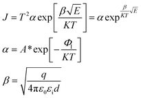
When the metal electrode is in contact with the ferroelectric thin film, a Schottky barrier is formed between the metal electrode and ferroelectric thin film because of their different work functions (work functions). When the work function of a metal is less than that of a semiconductor, free electrons in the metal are injected into ferroelectric thin films under the action of high temperature and strong electric field. The transport properties of these electrons are influenced by barrier height, temperature field, and electric field. Usually, the Schottky emission model is used to explain the conduction mechanism of carriers at the interface between a metal and ferroelectric thin films. The corresponding expression is20,21
 | (1) |
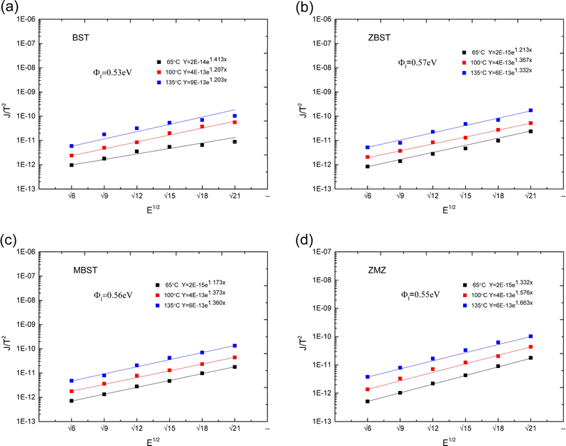 | ||
| Fig. 3 J/T2–E1/2 characteristic curves and corresponding fitting equations of all films ((a) BST; (b) ZBST; (c) MBST; (d) ZMZ). | ||
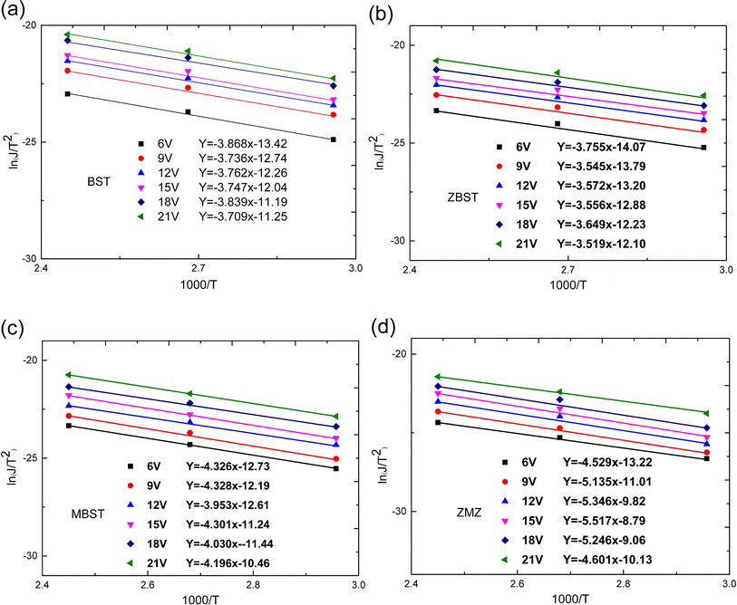 | ||
| Fig. 4 Ln(J/T2)–1000/T characteristic curves and corresponding fitting equations of BST, MBST, ZBST and ZMZ thin film ((a) BST; (b) ZBST; (c) MBST; (d) ZMZ). | ||
Take  and J/T2 as horizontal and vertical coordinates respectively, and then use Origin software to fit the curve exponentially. The fitting equation is y = aebx, and a = α,
  At this time, the parameters α, β and εi can be obtained. Then the refractive index of each film is obtained from formula εi = ns2 (ns is the refractive index parameter extracted under Schottky emission model).22 εi and ns are listed in Table 1. Because Richardson constant is influenced by thin film materials and electrode materials, the height of interface barrier can be calculated by Arrhenius formula.
| BST | ZBST | MBST | ZMZ | |
|---|---|---|---|---|
| εi | 4.123 | 1.145 | 1.210 | 1.613 |
| ns | 2.03 | 1.07 | 1.10 | 1.27 |
We used  and ln(J/T2) as horizontal and vertical coordinates, respectively, and then used Origin software to fit the curve exponentially. The fitting equations are y = kx + band b = ln
![[thin space (1/6-em)]](https://www.rsc.org/images/entities/char_2009.gif) C.
C.  was obtained using the formula
  The interface barrier height ΦI of each film was obtained by substituting the parameters obtained from the above fitting, and the results are shown in Fig. 3. The data in the figure show that the interface barrier heights of single-component acceptor-doped films (MBST, ZBST) and binary alternately doped films (ZMZ) are slightly higher than those of the undoped BST films. Compared with the MBST, ZBST, and ZMZ films, the interfacial barrier height of the binary alternately doped films (0.55 eV) is not much different from that of the single-component acceptor-doped films. This result shows that binary alternately doped films have little influence on the interfacial barrier height, which may be caused by the difference in surface state density at the surface of binary alternately doped films and that at the surface of single-component acceptor-doped films.23 In addition, compared with the results reported by Zafar et al., our results are small, which may be caused by factors such as film composition, calculation method, or fitting error.6
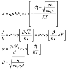
Because of thermodynamic fluctuations, some valence electrons bound by covalent bonds in an insulator or semiconductor atom may be excited to the conduction band, thus leaving the atom bound by another adjacent atom, which will form a weak conductance in the process. However, when the insulator or semiconductor is in a strong electric field, the number of electrons located on the impurity level (trap) will change (trap effect). For example, the energy required for electron excitation on the impurity (trap center)-Fe3+ existing in BaTiO3 will be greatly reduced. Therefore, a large number of electrons located in the center of the trap are excited to the conduction band, which eventually leads to a significant increase in its conductivity.24,25 This is a typical Poole–Frenkel conduction mechanism dominated by valence electrons in the thermal excitation binding center under a strong electric field. The change in the current density with temperature and electric field obeys the following expression:26,27
 | (2) |
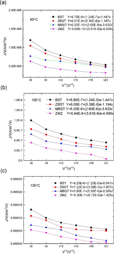 | ||
| Fig. 5 J/V–V1/2 and ln(J/V)–1000/T characteristic curves and corresponding fitting equations of BST, MBST, ZBST and ZMZ thin film ((a) 65 °C; (b) 100 °C; (c) 135 °C). | ||
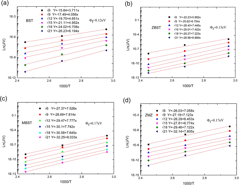 | ||
| Fig. 6 Ln(J/V)–1000/T characteristic curves and corresponding fitting equations of BST, MBST, ZBST and ZMZ thin film ((a) BST; (b) MBST; (c) ZBST; (d) ZMZ). | ||
Take  and
and  as horizontal and vertical coordinates respectively, and then use Origin software to fit the curve exponentially. The fitting equation is y = aebx, and a = α,
  At this point, parameters α, β and εi can be obtained. Then the refractive index of each film is obtained from formula εi = np2 (np is the refractive index parameter extracted under Poole–Frenkel model),22 and εi and np are listed in Table 2. Because the carrier mobility and carrier concentration in the thin film are unknown, the height of trap barrier in the thin film is also calculated by Arrhenius formula.
| BST | ZBST | MBST | ZMZ | |
|---|---|---|---|---|
| εi | 45.3 | 4.93 | 7.13 | 7.45 |
| np | 6.73 | 2.22 | 2.67 | 2.73 |
We used  and ln(J/E) as horizontal and vertical coordinates, respectively, and then used Origin software to fit the curve exponentially. The fitting equations are y = kx + band b = ln
![[thin space (1/6-em)]](https://www.rsc.org/images/entities/char_2009.gif) C. In this case,
C. In this case,  was obtained using the formula
  The trap barrier height of each film was obtained by substituting the above fitted parameters, and the results are shown in Fig. 6. The figure shows that the trap barrier heights of single-component acceptor-doped films (MBST, ZBST) and binary alternating-doped films (ZMZ) are higher than those of undoped BST films, and binary alternating-doped films have the largest trap barrier height (0.17 eV). Compared with MBST, ZBST and ZMZ films, it is found that the trap barrier height of each film is between 0.15 eV and 0.17 eV, which is close to the energy level of oxygen vacancy (0.15 eV), which indicates that the trap barrier height in the film may be related to the state of oxygen vacancy defects.16,28 By comparing the data in Tables 1 and 2, it can be seen that the refractive index ns of the BST films extracted by the Schottky emission model is closer to the experimental value of 2.2, while the refractive index np of the ZBST, MBST, and ZMZ films extracted by the Poole–Frenkel model are closer to the experimental value of 2.2. Therefore, Schottky–Simmons should be the main form of leakage conductance in BST films. The Poole–Frenkel conduction mechanism should be the main form of leakage conductance in the ZBST, MBST, and ZMZ films.
In order to explore the mechanism by which oxygen vacancy defects affect barrier height, we discuss the related mechanism from the following aspects. When doping ions (Zn2+, Mg2+) replace Ti4+ at site B, extrinsic oxygen vacancies and doping ions are simultaneously introduced into the lattice at the same time. The corresponding defect equation is as follows:
 | (3) |
 | (4) |
 is a cation vacancy with two negative charges,
  and
and  are acceptor-doped ions with two negative charges, and
  is an extrinsic oxygen vacancy with two unit positive charges.
According to the above defect equation, zinc and magnesium ions are the acceptor ions. However, when acceptor impurity ions are introduced into pure BST thin films, not only does the number of electrons ionized by donor oxygen vacancies and enter the conduction band decrease, but also the number of electrons located in the trap center decreases because of the compensation effect of acceptor impurities. Therefore, the trap effect in the thin film and the donor effect caused by the oxygen vacancy defects are weakened. Finally, the interface barrier heights of single-component acceptor-doped BST films and binary alternately doped films were higher than those of undoped BST films. The interface barrier height of the single-component acceptor-doped BST films is slightly higher than that of the binary alternating-doped films, which may be related to the different surface state densities at the film surface.23 Compared with single-component acceptor doped films, binary alternating doped films not only introduce acceptor zinc ions, but also acceptor magnesium ions, which is equivalent to introducing more types of acceptor impurity ions. Therefore, the compensation effect of acceptor impurities in the films is stronger, and the trap effect in the films is weakened, which increases the trap barrier height of the films.
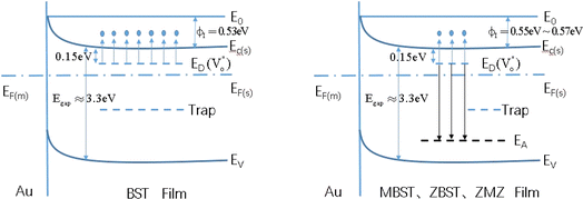
Finally, to relate the oxygen vacancy defect with the change in interface barrier height and trap barrier height, we draw a simplified energy band diagram based on the previous literature data and the data in this study, as shown in Fig. 7. The physical meanings represented by each physical quantity in the figure are as follows: E0 is the vacuum energy level, EC(s) is the conduction band of the semiconductor thin film, Ev(s) is the valence band of the semiconductor thin film, EF(m) is the Fermi level of gold, EF(s) is the Fermi level of the semiconductor thin film, and ΦI is the height of the interfacial barrier of the thin film. ED is the donor energy level, which refers to the energy level  corresponding to the oxygen vacancy defect; each short segment corresponds to a donor impurity atom. EA is the acceptor energy level and each short segment corresponds to an acceptor impurity atom. Where Egap is the bandgap width of the film.
Among them, for un-doped BST films, the band gap is about 3.3 eV (Egap = Ec(s) − Ev(s)), and the Fermi level (EF(s)) is not far from the bottom of the conduction band.7,29,30 The energy level of the oxygen vacancy defect is 0.15 eV below the conduction band bottom, which is close to the conduction band bottom.16,28
4. Conclusions
Experimental and calculation studies of single-composition acceptor-doped and multilayer acceptor-doped BST films were conducted. The results showed that the interface barrier height in the ZMZ film is 0.55 eV, which is higher than that of the un-doped BST film (0.53 eV), but the increase of the interface barrier height is not obvious compared with the single-component acceptor doped BST film. The trap barrier height in ZMZ thin film is 0.17 eV, which is higher than that of un-doped BST film (0.12 eV), and also higher than that of single-component acceptor doped BST film (0.15 eV). The increase in the trap height in the ZMZ films is related to the variation in the oxygen vacancy defect concentration. These results are of great interest for tunable microwave/radio frequency devices, where a very high level of understanding is needed regarding leakage current behavior, in order to comply with the specifications of such components.Data availability
We confirm that the data supporting the findings of this study are available within the article.Conflicts of interest
We declare no competing interests exist.Acknowledgements
This work was sponsored by the Shanghai DianJi University Talent Introduction and Scientific Research Start-up Project (grant no. B1-0288-22-007-05-008), the Shanghai University Students' Innovation and Entrepreneurship Training Program Project (grant no. S202211458041), the “Chen Guang” project supported by Shanghai Municipal Education Commission and Shanghai Education Development Foundation (15CG62).References
- M. L. V. Mahesh, P. Pal, V. V. B. Prasad and A. R. James, Fatigue and leakage current characteristics of lead free bilayer thin film structures, Ceram. Int., 2022, 48, 9006–9013 CrossRef CAS.
- P. T. M. Nguyen, T. Nguyen, M. D. Nguyen and T.-H. Vu, Impact of electrode materials on microstructure, leakage current and dielectric tunable properties of lead-free BSZT thin films, Ceram. Int., 2021, 47, 23214–23221 CrossRef CAS.
- B. Vigneshwaran, P. Kuppusami and S. Ajith Kumar, Structural and optical properties of Ba0.5Sr0.5TiO3 thin films on single crystalline substrates, Mater. Sci. Semicond. Process., 2022, 148, 106795 CrossRef CAS.
- K. P. Andryushin, L. A. Shilkina, S. V. Khasbulatov, A. V. Nagaenko, S. I. Dudkina, I. N. Andryushina, K. Sadykov, I. A. Verbenko, A. G. Rudskaya and L. A. Reznichenko, The effects of the modification of the BST-system solid solutions with rare earth elements, Ceram. Int., 2022, 48, 1642–1658 CrossRef CAS.
- X. H. Zhu, E. Defaÿ, M. Aïd, Y. J. Ren, C. Y. Zhang, J. L. Zhu, J. G. Zhu and D. Q. Xiao, Preferential growth and enhanced dielectric properties of Ba0.7Sr0.3TiO3thin films with preannealed Pt bottom electrode, J. Phys. D: Appl. Phys., 2013, 46, 105301 CrossRef.
- S. Zafar, R. E. Jones, B. Jiang, B. White, V. Kaushik and S. Gillespie, The electronic conduction mechanism in barium strontium titanate thin films, Appl. Phys. Lett., 1998, 73, 3533–3535 CrossRef CAS.
- J. Robertson and C. W. Chen, Schottky barrier heights of tantalum oxide, barium strontium titanate, lead titanate, and strontium bismuth tantalate, Appl. Phys. Lett., 1999, 74, 1168–1170 CrossRef CAS.
- Y.-P. Wang and T.-Y. Tseng, Electronic defect and trap-related current of (Ba0.4Sr0.6) TiO3 thin films, J. Appl. Phys., 1997, 81, 6762–6766 CrossRef CAS.
- C. Sudhama, J. Kim, J. Lee, V. Chikarmane, W. Shepherd and E. R. Myers, Effect of lanthanum doping on the electrical properties of solgel derived ferroelectric lead–zirconate–titanate for ultralargescale integration dynamic random access memory applications, J. Vac. Sci. Technol., B: Microelectron. Nanometer Struct.--Process., Meas., Phenom., 1993, 11, 1302–1309 CrossRef CAS.
- S. Y. Lee and T. Y. Tseng, Electrical and dielectric behavior of MgO doped Ba0.7Sr0.3TiO3 thin films on Al2O3 substrate, Appl. Phys. Lett., 2002, 80, 1797–1799 CrossRef CAS.
- S. S. Kim and C. Park, Leakage current behaviors of acceptor and donor-doped (Ba0.5Sr0.5)TiO3 thin films, Appl. Phys. Lett., 1999, 75, 2554–2556 CrossRef CAS.
- Z. J. Ma, T. J. Zhang and J. Y. Wang, Electrical properties and extension mechanism of Ohmic region of sol–gel derived Ba0.7Sr0.3TiO3 thin films by Zn doping, J. Mater. Sci.: Mater. Electron., 2011, 22, 862–865 CrossRef CAS.
- R. Meyer, R. Liedtke and R. Waser, Oxygen vacancy migration and time-dependent leakage current behavior of Ba0.3Sr0.7TiO3 thin films, Appl. Phys. Lett., 2005, 86, 112904 CrossRef.
- K. H. Ahn, S. Baik and S. S. Kim, Significant suppression of leakage current in (Ba,Sr)TiO3 thin films by Ni or Mn doping, J. Appl. Phys., 2002, 92, 2651–2654 CrossRef CAS.
- M. Copel, J. D. Baniecki, P. R. Duncombe, D. Kotecki, R. Laibowitz, D. A. Neumayer and T. M. Shaw, Compensation doping of Ba0.7Sr0.3TiO3 thin films, Appl. Phys. Lett., 1998, 73, 1832–1834 CrossRef CAS.
- J. P. B. Silva, K. C. Sekhar, A. Almeida, J. A. Moreira, M. Pereira and M. J. M. Gomes, Effects of oxygen partial pressure on the ferroelectric properties of pulsed laser deposited Ba0.8Sr0.2TiO3 thin films, Appl. Phys. A: Mater. Sci. Process., 2013, 113, 817–824 CrossRef CAS.
- S. Zafar, B. Hradsky, D. Gentile, P. Chu, R. E. Jones and S. Gillespie, Resistance degradation in barium strontium titanate thin films, J. Appl. Phys., 1999, 86, 3890–3894 CrossRef CAS.
- H. Z. Wang and B. Li, Effect of internal interface layer on dielectric properties of doped Ba0.6Sr0.4TiO3 thin films and its simulation in filters, J. Phys.: Condens. Matter, 2023, 35, 365002 CrossRef PubMed.
- D. Ravelosona, S. Mangin, Y. Lemaho, J. A. Katine, B. D. Terris and E. E. Fullerton, Domain wall creation in nanostructures driven by a spin-polarized current, Phys. Rev. Lett., 2006, 96, 186604 CrossRef CAS.
- L. Pintilie and M. Alexe, Metal-ferroelectric-metal heterostructures with Schottky contacts. I. Influence of the ferroelectric properties, J. Appl. Phys., 2005, 98, 124103 CrossRef.
- L. Pintilie, I. Vrejoiu, D. Hesse and M. Alexe, The influence of the top-contact metal on the ferroelectric properties of epitaxial ferroelectric Pb(Zr0.2Ti0.8)O3 thin films, J. Appl. Phys., 2008, 104, 114101 CrossRef.
- J. G. Simmons, Poole-Frenkel Effect and Schottky, Effect in Metal-Insulator-Metal Systems, Phys. Rev., 1967, 155, 657–660 CrossRef CAS.
- J. F. Scott, Dielectric breakdown in high-ε films for ulsi DRAMs: III. Leakage current precursors and electrodes, Integr. Ferroelectr., 1995, 9, 1–12 CrossRef CAS.
- E. Siegel and K. A. Müller, Structure of transition-metal-oxygen-vacancy pair centers, Phys. Rev. B: Condens. Matter Mater. Phys., 1979, 19, 109–120 CrossRef CAS.
- M. Actis and F. Michel-Calendini, Impurity levels and nonlinear optical properties of doped BaTiO3 from extended cluster LDA calculations, Int. J. Quantum Chem., 1997, 61, 657–664 CrossRef CAS.
- P. Zubko, D. J. Jung and J. F. Scott, Electrical characterization of PbZr0.4Ti0.6O3 capacitors, J. Appl. Phys., 2006, 100, 114113 CrossRef.
- P. Zubko, D. J. Jung and J. F. Scott, Space charge effects in ferroelectric thin films, J. Appl. Phys., 2006, 100, 114112 CrossRef.
- A. Vorobiev, P. Rundqvist, K. Khamchane and S. Gevorgian, Microwave loss mechanisms in Ba0.25Sr0.75TiO3 thin film varactors, J. Appl. Phys., 2004, 96, 4642–4649 CrossRef CAS.
- J. Robertson, Band offsets of wide-band-gap oxides and implications for future electronic devices, J. Vac. Sci. Technol., B: Microelectron. Nanometer Struct.--Process., Meas., Phenom., 2000, 18, 1785 CrossRef CAS.
- X. F. Liang, Z. Y. Meng and W. B. Wu, Effect of Acceptor and Donor Dopants on the Dielectric and Tunable Properties of Barium Strontium Titanate, J. Am. Ceram. Soc., 2004, 87, 2218–2222 CrossRef CAS.
| This journal is © The Royal Society of Chemistry 2024 |

