 Open Access Article
Optimizing the optoelectronic properties of broadband FeS2/Si photodetectors via deposition temperature tuning in chemical bath deposition
Mustafa W. Fatehia,
Huda Saadi Alib and
Raid A. Ismail *c
*c
aCollege of Education for Pure Sciences, University of Tikrit, Iraq
bCollege of Energy and Environmental Sciences, Al-Karkh University of Science, Baghdad, Iraq
cDepartment of Applied Science, University of Technology, Baghdad, Iraq. E-mail: raidismail@yahoo.com
First published on 20th November 2024
Abstract
This study investigates the fabrication and characterization of n-FeS2/p-Si heterojunction photodetectors using chemical bath deposition (CBD) at deposition temperatures ranging from 50 °C to 80 °C. The impact of temperature on the structural, morphological, and optical properties of FeS2 thin films was evaluated. X-ray diffraction (XRD) revealed polycrystalline cubic FeS2 with improved crystallinity as the deposition temperature increased. The optical energy gaps of the films ranged from 2.41 eV to 1.6 eV, decreasing with higher temperatures. Scanning electron microscopy (FE-SEM) showed that grain size increased from 30 nm to 180 nm as the temperature rose. Hall effect measurements confirmed the n-type conductivity of the film, with mobility decreasing from 5 to 3.17 cm2 V−1 s−1 at higher temperatures. The heterojunctions exhibited rectifying behavior, with the best ideality factor of 1.7 observed at 60 °C. The photodetector fabricated at 60 °C showed superior performance, with a responsivity of 0.37 A W−1 at 520 nm and 0.7 A W−1 at 770 nm, an external quantum efficiency of 52%, and a detectivity of 8 × 10¹¹ Jones at 520 nm, making it the optimal configuration for efficient broadband photodetection.
1. Introduction
Iron pyrite (β-FeS2) is a promising semiconducting material with an indirect optical energy gap of 0.9 eV and a cubic structure (Pa![[3 with combining macron]](https://www.rsc.org/images/entities/char_0033_0304.gif) space group). It is widely used in various industrial and technological applications such as photovoltaic solar cells,1–3 batteries,4 photoemission,5 and photodiodes.6–9 This widespread use is due to its excellent optical properties, including a high absorption coefficient (α > 105 cm−1 for hv > 1.3 eV),10 as well as a long minority carrier diffusion length (100–1000 nm), which make it suitable for optoelectronic devices.9–11 Compared to other semiconductors, FeS2 nanocrystals are inexpensive, eco-friendly, and abundant, with iron being the fourth most abundant element in the Earth's crust. These attributes make FeS2 an ideal candidate for the development of affordable optoelectronic devices.
space group). It is widely used in various industrial and technological applications such as photovoltaic solar cells,1–3 batteries,4 photoemission,5 and photodiodes.6–9 This widespread use is due to its excellent optical properties, including a high absorption coefficient (α > 105 cm−1 for hv > 1.3 eV),10 as well as a long minority carrier diffusion length (100–1000 nm), which make it suitable for optoelectronic devices.9–11 Compared to other semiconductors, FeS2 nanocrystals are inexpensive, eco-friendly, and abundant, with iron being the fourth most abundant element in the Earth's crust. These attributes make FeS2 an ideal candidate for the development of affordable optoelectronic devices.
However, the application of FeS2 films in optoelectronic devices has been limited due to their poor output efficiency.8,12–14 The generation of electronic states within the optical energy gap is believed to result from impurities or sulfur vacancies, both in the bulk and on the surface.15,16 Extensive efforts have been made to enhance the optoelectronic properties of FeS2 by focusing on synthesis, doping, and surface passivation.8,9 Nanostructured FeS2 has demonstrated superior physical and chemical properties compared to its bulk counterpart. Various methods have been employed to prepare FeS2 nanostructure films, including thermal decomposition,17 electrodeposition,18 laser deposition,19 spray pyrolysis,20 microwave-assisted methods,21 magnetron sputtering,22 chemical vapor deposition (CVD),23 and chemical bath deposition (CBD).24
One of the most promising routes for the preparation of FeS2 nanostructures is the chemical bath deposition (CBD) method. This technique offers several advantages over other deposition methods: it is simple, cost-effective, does not require a vacuum, allows for large-area deposition, and provides good control over film thickness and stoichiometry.25 Heterojunction-based silicon photodetectors have demonstrated significantly better optoelectronic properties compared to homojunctions silicon photodetectors. These heterojunction photodetectors exhibit high responsivity, a wide spectral response, low noise, a large minority carrier diffusion length, operation at high bias voltages, excellent linearity, and fast response times. Various types of heterojunction-based silicon photodetectors have been prepared using the CBD method, including CdO/Si,26 Sb2S3/Si,27 CdS/Si,28 Cu2S/Si,29 and SnO2/Si.30 The performance of these photodetectors is highly dependent on the optical and electrical properties of the films, as well as the preparation method and conditions.
In the CBD process, substrate temperature is a critical preparation parameter. It plays a vital role in the adhesion of the film to the silicon substrate, film thickness, and crystallinity.31 Varying the deposition temperature can alter the film's morphology, optical properties, and chemical composition, thereby affecting the growth and nucleation mechanisms of thin films. This can lead to preferred growth orientations, resulting in changes in the optical and structural properties of the films and, consequently, the performance of the photodetectors. FeS2 has a lattice constant of 5.417 Å, which is close to that of single-crystal silicon (5.429 Å), indicating a small lattice mismatch. This minimizes the likelihood of strain and structural defects at the FeS2/Si interface. Actually, the optical bandgap of FeS2 nanostructure can be tuned by varying the deposition conditions, such as temperature. This tunability allows the photodetectors to operate over a broad spectral range, from visible to near-infrared (NIR). One of the most important advantages of FeS2/Si photodetectors is the ability to control the stoichiometry of FeS2 films through deposition temperature. This allows fine-tuning of electrical and optical properties, which directly impact device performance.
Here, we report on the optimization of deposition temperature for fabricating high-performance FeS2/Si heterojunction photodetectors using the chemical bath deposition (CBD) method, without the need for a buffer layer. This approach simplifies the fabrication process, making it cost-effective and scalable while maintaining excellent heterojunction quality. The systematic investigation of deposition temperatures enables the identification of optimal conditions for enhancing the structural, optical, and electrical properties of FeS2 films. Additionally, the observed dual-peak photodetection response, with one peak being tunable by deposition temperature, introduces a novel feature that enhances the versatility of FeS2/Si photodetectors for broadband and selective photodetection. This work provides new insights into the relationship between deposition conditions and device performance, demonstrating the potential of FeS2/Si heterojunctions for efficient visible and near-infrared light detection.
2. Experimental procedure
2.1. Deposition of FeS2 films
FeS2 thin films were deposited on corning glass and silicon substrates using the chemical bath deposition (CBD) technique. First, the glass substrate was cleaned with methanol and deionized water (DI) in an ultrasonic bath for 20 minutes and then dried with nitrogen gas. The silicon substrate used was a one-side p-type (boron-doped silicon) polished surface with (100) orientation and an electrical resistivity of 14–22 Ω cm. The selection of a high-resistivity silicon substrate is intended to reduce leakage current in the photodetector. This enhances the signal-to-noise ratio, allowing for better photosensitivity and lower dark current in the FeS2/Si photodetector. A low doping concentration helps reduce free carrier absorption and promotes efficient transport of photogenerated carriers, which in turn increases the photocurrent and enhances the overall performance of the photodetector.All chemicals utilized in this study are of high purity and were not subjected to further purification. To prepare the solution for FeS2 thin film deposition, 10 ml of 1 M FeSO4 (iron sulfate, 99.9% purity provided from Vans Medical Co.) was placed in a 50 ml glass flask, followed by the addition of 3 ml of 1 M ethylenediaminetetraacetic acid (EDTA purchased from Thomas Baker Co.) and ammonia (NH3). Next, 10 ml of 1 M CS(NH2)2 (99.9% purity provided from CDH Co.) was added to the mixture and stirred for 5 minutes. Finally, 30 ml of distilled water was added to the solution, with FeSO4 serving as the source of Fe2+ ions and CS(NH2)2 as the precursor for S2− ions.
The films were deposited at various deposition temperatures, ranging from 50 to 80 °C in 10 °C increments. As the deposition temperature increased from 50 to 80 °C, a gradual change in the color of the solution was observed, transitioning from gray to yellow and then to reddish-brown, as shown in Fig. 1. The deposition time was fixed at 60 minutes. After the deposition process was completed, the films were placed in an oven at 100 °C for 15 minutes.
2.2. Characterization of FeS2 films
The optical properties of the FeS2 films deposited on glass substrates at different temperatures were measured using a UV-vis double-beam spectrophotometer (Shimadzu, 00912901-S). The structural properties of the FeS2 films were examined using an X-ray diffractometer (Malvern Panalytical). A field emission scanning electron microscope (FE-SEM) equipped with energy-dispersive X-ray spectroscopy (EDX) was used to investigate the structural and chemical composition of the FeS2 films. The surface topography and roughness of the deposited films were analyzed using atomic force microscopy (AFM, TT-2AFM). The thickness of the films was measured using cross-sectional images obtained from the FE-SEM.2.3. Fabrication and characterization of FeS2/Si heterojunction photodetector
The photodetector was fabricated by depositing FeS2 thin films onto the polished side of silicon substrates at different deposition temperatures using a thermal evaporation system. An interdigitated mask was employed to define the patterned regions for the metal contacts, ensuring precise alignment of the contact electrodes. Ohmic contacts were formed on both the FeS2 film and the backside of the silicon substrate by evaporating silver (Ag) and aluminum (Al) films, respectively. The thermal evaporation process was carried out under a vacuum pressure as low as 10−6 mbar. The silicon substrates were heated to a temperature of 100 °C during the deposition of the electrodes to improve film adhesion and uniformity. Fig. 2a shows the schematic diagram of the cross-sectional view of the In–FeS2/Si–Al photodetector. The current–voltage characteristics of the FeS2/Si heterojunction were measured in both dark and illuminated conditions.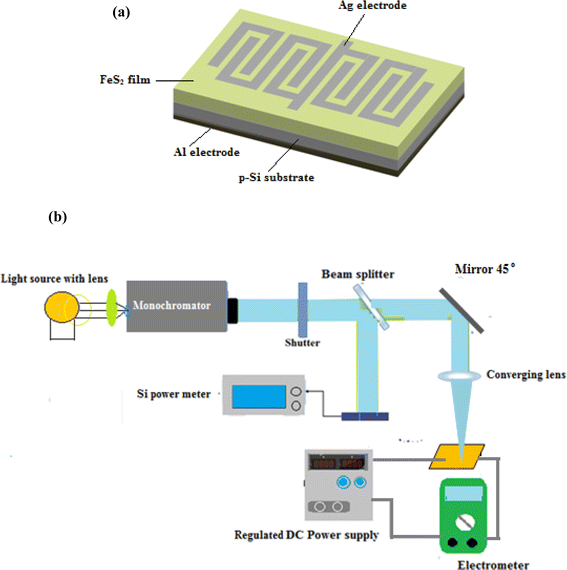 | ||
| Fig. 2 (a) Cross section view of FeS2/Si photodetector and (b) schematic diagram of cross-sectional view of the Ag–FeS2/n-Si–Al photodetector. | ||
The spectral responsivity of the photodetectors, fabricated at various deposition temperatures, was evaluated in the wavelength range of 430–900 nm using a photodetector evaluation system. This system included a halogen lamp with a focusing setup and a DC power supply. Fig. 2b shows the schematic diagram of setup used to measure the parameters of the photodetector.
3. Results and discussion
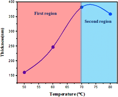
Fig. 3 shows the variation in film thickness as a function of deposition temperature. The film thickness was measured from the SEM images of the film cross-section. The thickness of the film increases with deposition temperature, rising sharply (first region) up to 70 °C, and then slightly decreasing as the temperature is further increased to 80 °C (second region).The initial increase in film thickness with temperature is attributed to the higher kinetic energy of the molecules involved in the reaction, which leads to an accelerated reaction rate and more rapid formation and deposition of the film material. Additionally, elevated temperatures enhance nucleation rates, improve sedimentation, and promote more complete evaporation, all contributing to a faster growth rate and an increase in the thickness of the FeS2 film. Further increases in the solution temperature result in a decrease in film thickness due to the decomposition of chemical precursors and/or the formation of volatile by-products, which do not deposit as a solid film. This reduction in material available for deposition leads to thinner films.32 Fig. 4 shows SEM images of the cross-sectional view of FeS2 films deposited on silicon substrates at different temperatures. The images reveal clear boundaries between the deposited films and the silicon substrate. It can be observed that the film thickness is not uniform across the substrate, with noticeable clustering and agglomeration of grains affecting the deposition.
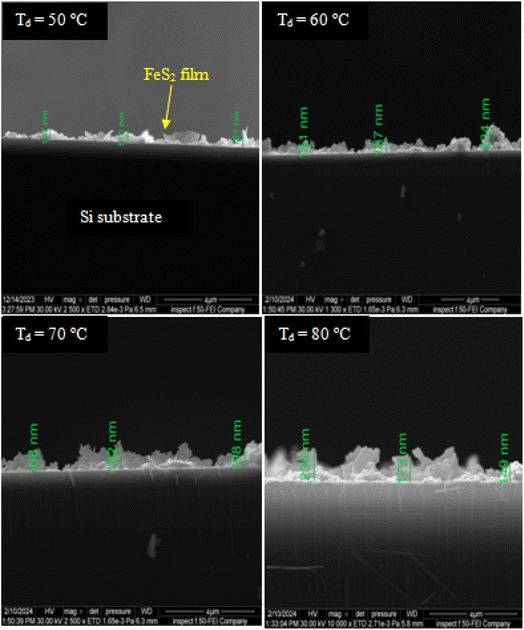 | ||
| Fig. 4 SEM images cross section of FeS2 films deposited on silicon substrates at various temperatures. | ||
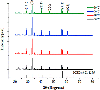
Fig. 5 shows the X-ray diffraction (XRD) pattern of FeS2 thin films deposited at various temperatures.
As illustrated, six peaks are observed at 2θ = 28.3°, 33.79°, 41.81°, 47°, 56.7°, and 61.3°, corresponding to the (111), (200), (211), (220), (311) and (023) planes, respectively. These peaks are indexed to cubic FeS2, in accordance with JCPDs # 01-1295. The degree of crystallinity of the film improved with increasing deposition temperature up to 70 °C. However, further increases in temperature led to a deterioration in crystal quality. This decline is attributed to the reduction in film thickness at 80 °C and the formation of finer grains. The crystallite size of the films was evaluated using the Debye–Scherrer equation and is listed in Table 1. It is observed that the crystallite size increases with the deposition temperature up to 70 °C and then decreases at 80 °C. This result can be attributed to the fact that, at higher deposition temperatures, the reaction kinetics increase, leading to faster nucleation of new crystallites. As a result, a greater number of smaller crystallites form, as the available material is distributed across more nuclei. Film's lattice constant was also determined as a function of temperature and found to be consistent with bulk FeS2.33
| Td (°C) | Lattice constant (A) | Crystallite size (nm) |
|---|---|---|
| 50 | 5.41 | 33 |
| 60 | 5.43 | 38 |
| 70 | 5.45 | 43 |
| 80 | 5.49 | 28 |
Fig. 6 illustrates the effect of deposition temperature on the optical absorbance of FeS2 films. The optical absorption decreases sharply as the wavelength increases beyond 300 nm and then levels off at wavelengths dependent on the deposition temperature.
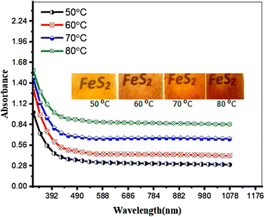 | ||
| Fig. 6 Effect of deposition temperature on the optical absorbance of FeS2 film. Inset is the photographs of films deposited at various deposition temperatures. | ||
The absorption edges for films deposited at 50, 60, 70, and 80 °C are observed at 440, 455, 525, and 576 nm, respectively. This red shift is attributed to the increase in film thickness and grain size. Additionally, particle aggregation in films deposited at higher temperatures leads to decreased optical transmission due to scattering. The inset of Fig. 4 shows photographs of FeS2 films deposited at different temperatures, with color changing from yellow to brown, reflecting the different absorption edges. Furthermore, film uniformity slightly decreases and transparency reduces as the deposition temperature increases.34
Fig. 7 shows the variation of (αhν)2 versus photon energy (hν) for FeS2 films deposited at various temperatures. The optical energy gap (Eg) of the films was determined by extrapolating the linear portion of this plot to the (αhν)2 = 0 point, according to the Tauc plot35
| (αhν) = A(hν − Eg)n | (1) |
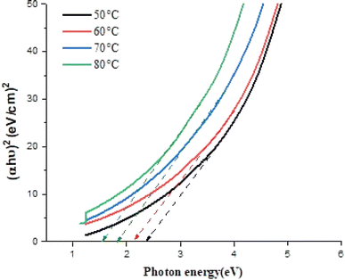 | ||
| Fig. 7 Plot of (αhν)2 versus photon energy of FeS2 films deposited at different temperature using laser. | ||
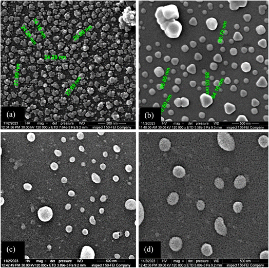
The optical energy gap decreases as the deposition temperature increases due to the increase of grain size, change in film stoichiometry, and structural defects. Fig. 8 depicts SEM images of FeS2 films deposited at different temperatures. The morphology of all films consists of grains with various shapes and sizes, indicating a surface covered with distinct particles. This granular nature can influence the material's surface properties, such as roughness, and affect its optical and electronic characteristics.
The film deposited at 50 °C shows a high concentration of agglomerated grains with an average size of 20 nm, including some spherical particles. Nanograins, having high surface energy, tend to cluster together to minimize their overall surface energy. At lower temperatures, this clustering effect is more pronounced due to reduced particle mobility, which hinders the formation of a uniform film. The SEM images also reveal the presence of triangular grains, which may be related to specific crystallographic facets of FeS2, where certain crystal planes grow more readily than others, leading to characteristic shapes.
Fig. 9 displays the EDX spectra and analysis of FeS2 films deposited at different temperatures. The spectra confirm the presence of iron and sulfur, the primary elements of the films, along with additional peaks associated with silicon, sodium, oxygen, aluminum, and carbon from the glass substrate. For the film deposited at 50 °C, the atomic ratio of [S]/[Fe] is 1.11, while at 60 °C, the ratio is 1.07. These ratios indicate that the films are slightly off-stoichiometric, with a slight deficiency of sulfur relative to iron. At 70 °C, the ratio decreases to 0.83, signifying a non-stoichiometric film. By 80 °C, the atomic ratio further decreases to 0.66, also indicating a non-stoichiometric composition.
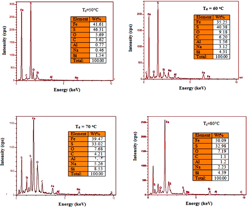 | ||
| Fig. 9 EDX spectra of FeS2 films deposited at different temperatures. Inset is the weight percentage of the elements in FeS2 film. | ||
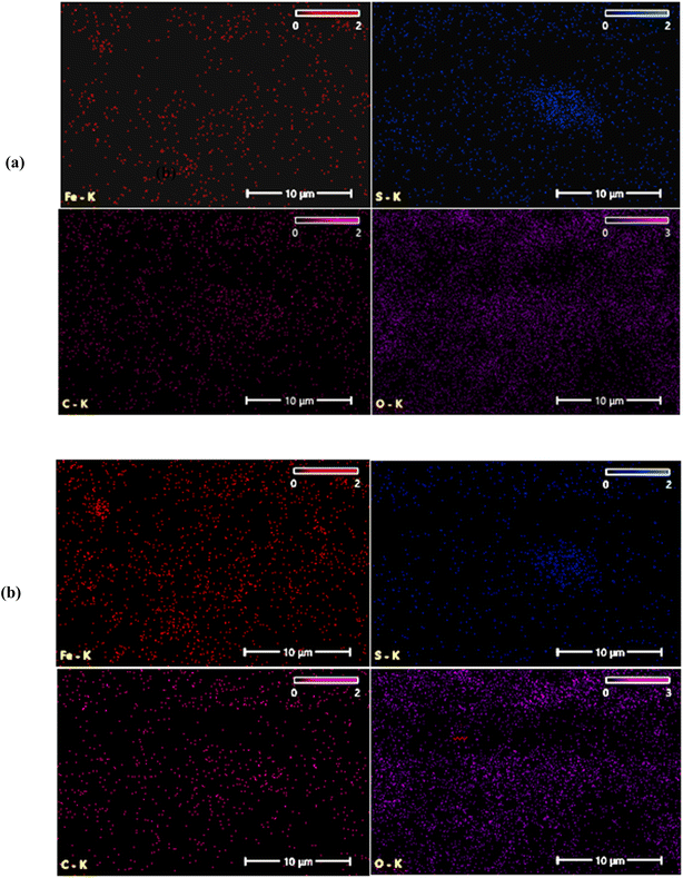
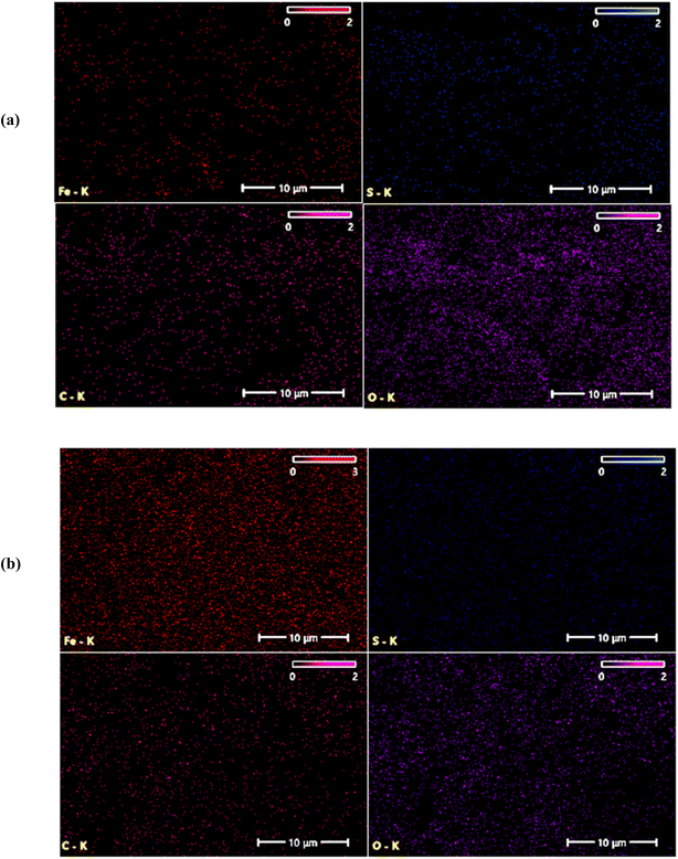
The films deposited at 70 °C and 80 °C exhibit a lower sulfur content relative to iron. This suggests that at higher deposition temperatures, sulfur may vaporize more readily than iron, leading to a lower sulfur-to-iron ratio in the final film.36 At 80 °C, the atomic ratio [S]/[Fe] decreases further to 0.66, indicating that the film is non-stoichiometric film. The films deposited at 70 °C and 80 °C show a lower sulfur content compared to iron. This suggests that at higher deposition temperatures, sulfur may vaporize more readily compared to iron, leading to reduce sulfur-to-iron ratio in the final film.36 EDX mapping of the FeS2 films deposited at various temperatures is shown in Fig. 10 and 11.
The Fe and S elements are uniformly distributed throughout the FeS2 films. However, as the deposition temperature increases, the concentration of Fe clearly increases, while the concentration of S decreases.
The effect of varying deposition temperatures on the surface topography of FeS2 was investigated using atomic force microscopy (AFM), as shown in Fig. 12. The AFM images confirm the growth of films with uniformly distributed grains across the surface.
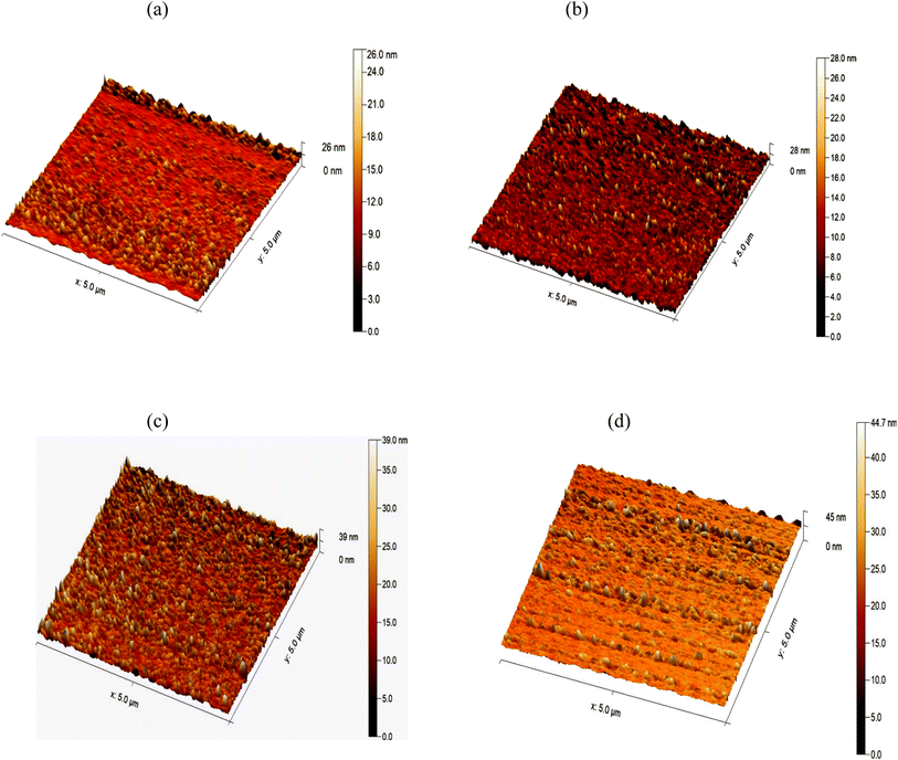 | ||
| Fig. 12 3-D AFM images of FeS2 films deposited at various temperatures (a) 50 °C, (b) 60 °C, (c) 70 °C, and (d) 80 °C. | ||
The film deposited at 50 °C, as illustrated in Fig. 12a, exhibits a smooth surface with a root mean square (RMS) roughness of 9.676 nm and an average grain size of 41.36 nm, as shown in Table 2. As the deposition temperature increases to 60 °C, as shown in Fig. 12b, the surface roughness rises to 22.52 nm, and the average grain size increases to 45.16 nm. The increase in RMS surface roughness can be attributed to the rapid nucleation and growth of the film at higher temperatures. The faster reaction rate leads to more irregular growth, which contributes to increased surface roughness. Despite this, the film surfaces are free of cracks and porosities, indicating uniform growth with evenly distributed grains.
| Temperature of solution (°C) | Average grain size (nm) | RMS of surface roughness (nm) |
|---|---|---|
| 50 | 41.36 | 9.676 |
| 60 | 45.16 | 22.52 |
| 70 | 53 | 38.09 |
| 80 | 64 | 49.71 |
At a deposition temperature of 70 °C, as depicted in Fig. 12c, the surface appears more homogeneous, with a noticeable increase in surface roughness and grain height. The RMS surface roughness is 38.09 nm, and the average grain size is 53.02 nm. These results suggest that increasing the deposition temperature improves grain uniformity and increases grain size, enhancing the film's topographical properties. At 80 °C, shown in Fig. 12d, the surface remains homogeneous with further increased surface roughness and particle height. The RMS surface roughness reaches 49.71 nm, and the average grain size grows to 64.27 nm. This increase reflects the effect of higher temperatures in promoting more effective nanoparticle growth and distribution. The surfaces remain free of cracks and porosities, indicating high-quality films at these deposition temperatures.37,38
The Hall measurement confirmed that the FeS2 films are of n-type, as indicated by their negative Hall coefficient. Fig. 13 shows the variation in electrical resistivity and mobility of FeS2 films as a function of deposition temperature. As the deposition temperature increases from 50 °C to 60 °C, both the resistivity decreases and the mobility increases. This improvement is attributed to enhanced crystallinity at higher temperatures, which leads to larger grain sizes and fewer defects such as grain boundaries or vacancies. These factors facilitate more efficient charge carrier movement, reducing resistivity and increasing mobility.
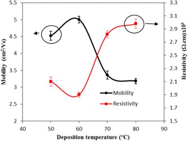 | ||
| Fig. 13 Variation of the electrical resistivity and mobility of FeS2 film with deposition temperature. | ||
In the second region, as the deposition temperature rises to 80 °C, the electrical resistivity of the film increases, and mobility decreases. This trend is likely due to the formation of a rougher, more porous film or grain growth that results in isolated grains with poor connectivity. Such changes can disrupt charge carrier pathways, leading to increased resistivity. Additionally, higher deposition temperatures may introduce more impurities from the deposition environment or precursor materials into the film. These impurities can create energy levels within the bandgap of FeS2, trapping charge carriers and contributing to increased resistivity and decreased mobility. Deviations from the ideal stoichiometry of the FeS2 film may also further contribute to the increased electrical resistivity.39
Fig. 14a shows the forward and reverse current–voltage characteristics of n-FeS2/p-Si heterojunctions fabricated at different deposition temperatures, within a voltage range of −10 to +10 V in the dark. Fig. 14b shows experimental and fitted I–V characteristics of heterojunction prepared at 60 °C, which are consistent with eqn (2).
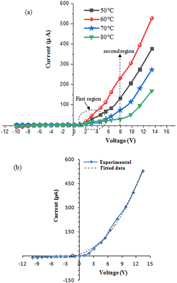 | ||
| Fig. 14 (a) Dark I–V characteristics of n-FeS2/p-Si heterojunctions prepared at various deposition temperatures and (b) experimental and fitted I–V curves for heterojunction deposited at Td = 60 °C. | ||
The FeS2/Si heterojunctions exhibit rectifying behavior, as evidenced by the forward currents being significantly larger than the reverse currents. In the reverse bias region, the current is relatively stable and independent of the bias voltage, which can be attributed to the widening of the depletion layer, increasing the junction resistance in the reverse direction. No soft breakdown was observed in the heterojunctions at voltages below 10 V. The forward current of the heterojunctions fabricated at Td = 60 °C was notably higher than that of the other heterojunctions. This enhancement is consistent with the lower electrical resistivity of FeS2 deposited at this temperature, as shown in Fig. 13.
The forward current–voltage characteristics for all samples exhibit exponential growth with increasing bias voltage, indicating that they follow the diode equation.
 | (2) |
The ideality factor of the heterojunctions, determined from eqn (2) and summarized in Table 3, varies with deposition temperature. The heterojunction fabricated at 60 °C exhibits the lowest ideality factor, indicating the best junction characteristics. An ideality factor approaching unity confirms optimal junction performance, where diffusion current is the primary transport mechanism. Conversely, a high ideality factor β > 1 suggests the presence of surface states and structural defects at the interface, which trap charge carriers and degrade junction performance. The turn-on voltage VT of the heterojunction was estimated and found to vary with deposition temperature, as depicted in Table 3. The heterojunction deposited at Td = 60 °C has VT of 3.4 V, while the heterojunction deposited at Td = 80 °C has VT = 4.7 V. These variations are attributed to the electrical resistivity of the FeS2 film, which influences the built-in-potential of the heterojunction.40
| Td (°C) | β | VT (V) |
|---|---|---|
| 50 | 5.3 | 4.7 |
| 60 | 1.7 | 3.4 |
| 70 | 2.2 | 3.9 |
| 80 | 4.5 | 4.7 |
Fig. 15 shows the effect of deposition temperature on the illuminated I–V properties of FeS2/Si heterojunction photodetectors under varying light intensities. When light is incident on the photodetector from the FeS2 side, it is absorbed in the depletion region near the FeS2 film, generating electron–hole (e–h) pairs. The holes move towards the silicon, while the electrons drift into the FeS2 film due to the internal electric field formed within the depletion region.
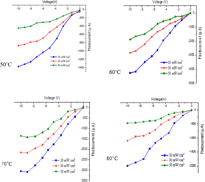 | ||
| Fig. 15 Illuminated I–V characteristics of n-FeS2/p-Si heterojunctions deposited at different temperatures. | ||
The maximum photocurrent is observed for the photodetector fabricated at Td = 60 °C, attributed to the highest electron mobility and lowest electrical resistivity of the FeS2 film at this temperature. This indicates efficient photogenerated carrier contribution to the photocurrent with minimal e–h recombination. This efficiency is primarily due to minimized grain boundaries and reduced carrier scattering within the film. The on/off ratio (photoelectric current to dark current ratio) of the photodetectors was calculated at a 10 V bias and a light density of 50 mW cm−2, yielding values of 115, 150, 87, and 22 for deposition temperatures of 50 °C, 60 °C, 70 °C, and 80 °C, respectively. As shown in Fig. 15, increasing light intensity leads to an increase in photocurrent, due to the higher number of photogenerated e–h pairs in the depletion region. Furthermore, increasing the bias voltage enhances the photocurrent of the photodetector by widening the depletion region, which facilitates more efficient charge carrier separation and collection41,42
The variation of the photocurrent of photodetectors deposited at different temperatures versus light intensity is illustrated in Fig. 16. As shown in this figure, two distinct regions can be observed: the first region is a low-intensity region where the photocurrent is linearly proportional to light intensity, and the second region shows that the photocurrent tends to saturate at high light intensity. This behavior can be attributed to the presence of trapping centers within the energy gap of the FeS2 films, which trap photogenerated carriers and lead to the saturation of photocurrent. This saturation, in turn, reduces the linear dynamic range (LDR) of the photodetector.
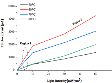 | ||
| Fig. 16 Variation of photocurrent with light intensity of n-FeS2/p-Si photodetectors deposited at different temperatures. | ||
The linear region at low light intensities indicates efficient photogenerated carriers and collection, suggesting that the photodetectors perform well under low-intensity illumination. However, as light intensity increases, trapping centers begin to dominate carrier dynamics. These centers act as recombination sites, preventing further increases in photocurrent despite the higher generation of electron–hole pairs. This saturation effect is a common limitation in photodetectors, particularly in materials where defect states or impurities create energy levels within the bandgap. To minimize the effects of photocurrent saturation and enhance the linear dynamic range (LDR), optimizing the deposition process to reduce the density of trapping centers is essential. This could involve adjusting the deposition temperature, refining growth conditions, or employing post-deposition annealing treatments to passivate defect and surface states in the FeS2 films. Notably, the photodetector prepared at 50 °C shows semi-linear behavior, which suggests that higher deposition temperatures may induce defects at the photodetector interface. Additionally, exploring different deposition temperatures in this study could reveal an optimal temperature that minimizes the density of these trapping centers, thereby enhancing the performance of the FeS2/Si photodetectors, especially in high-intensity environments.
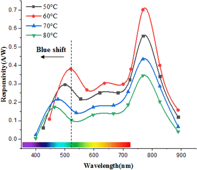
Fig. 17 illustrates the effect of deposition temperature on the spectral responsivity of FeS2/Si photodetectors. Two distinct peaks in the responsivity spectrum are observed: the first peak corresponds to the absorption edge of the FeS2 film, and the second peak at 770 nm is attributed to the absorption edge of the silicon substrate. The position of the first peak varies within the range of 460–520 nm, depending on the deposition temperature. This variation is due to changes in the optical energy gap with deposition temperature. An increase in the energy gap results in a shift of the peak response to shorter wavelengths (blue shift), while a decrease in the energy gap leads to a shift to longer wavelengths (red shift).43
The maximum responsivity of the photodetector fabricated at Td = 60 °C was 0.37 A W−1 at 520 nm and 0.7 A W−1 at 770 nm. The wavelengths longer than 520 nm are absorbed in the depletion region side inside the silicon substrate.44,45 As noted earlier, the film deposited at 60 °C has the lowest electrical resistivity and highest mobility, which enhances photodetection at both short and long wavelengths. This enhancement is attributed to the widening of the depletion region into FeS2 film and increased the diffusion length, since the diffusion length is given by  where μ is the mobility and τ is the minority lifetime.
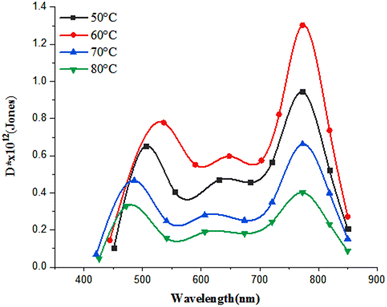
The specific detectivity of the photodetector as a function of deposition temperature is shown in Fig. 18.
The detectivity is defined as the minimum detectable power and it can be estimated from  , where A is the photosensitive area of the photodetector (A = 1 cm2) and Δf is the spectral bandwidth, and In is the noise current at certain bias voltage. The highest value of D* was 8 × 10¹¹ Jones at 520 nm (visible region) and 1.3 × 10¹² Jones at 770 nm (near infrared) for the FeS2/Si photodetector fabricated at 60 °C. After this temperature, the detectivity decreases due to the decreasing the responsivity and increasing the surface leakage current (noise current).46
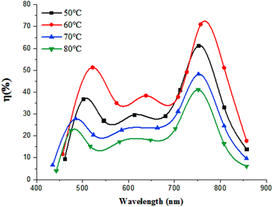
The variation of external quantum efficiency with wavelength of the photodetectors fabricated at various deposition temperatures is depicted in Fig. 19. The quantum efficiency can be calculated by  .
.
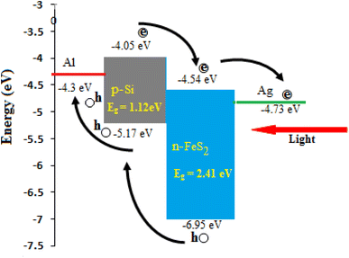
The photodetector prepared at 60 °C exhibits a quantum efficiency of 52% at 520 nm and 72% at 770 nm. This high quantum efficiency can be attributed to the effective collection of photogenerated carriers, which is facilitated by the large depletion layer width and the strong internal electric field.47–49 These factors contribute to minimizing electron–hole recombination, thereby enhancing the photodetector's performance. Additionally, the large surface area of the nanostructured film increases optical absorption, which improves the EQE.50,51 Fig. 20 depicts the illuminated energy band diagram of n-FeS2/p-Si heterojunction photodetector. The minimum energy levels of the conduction band EC and the valence band EV of the FeS2 film were determined to be −4.54 eV and −6.95 eV, respectively. The band offsets of the n-FeS2/p-Si heterojunction were calculated as follows:
| ΔEC = EC(Si) − EC(FeS2) = −4.05 eV − (−4.54 eV) = 0.49 eV |
| ΔEV = EV(Si) − EV(FeS2) = −5.17 eV − (−6.95 eV) = 1.78 eV |
As shown in Fig. 20, the Fermi level (EF) for both materials, n-FeS2 and p-Si, was determined based on their respective electron affinities and band gaps. The energy gap for n-FeS2 is Eg = 2.41 eV, while for p-Si, Eg = 1.12 eV. The electron affinity for n-FeS2 is approximately χ = 4.54 eV, and for p-Si, it is around χ = 4.05 eV. In equilibrium, the Fermi levels of the FeS2 and Si align, resulting in band bending near the interface. The Fermi level of n-FeS2 is calculated from the following equation and found to be 0.33 eV near the conduction band:
 | (3) |
Table 4 presents the key figures of merit for the FeS2/Si photodetector fabricated at a deposition temperature Td = 60 °C, compared with other silicon-based heterojunction photodetectors. The table highlights parameters such as responsivity, detectivity, and external quantum efficiency, offering a comprehensive comparison to assess the performance advantages of the FeS2/Si device over other similar photodetectors.
| Photodetector type | Preparation method | Peak wavelength (nm) | Responsivity Rλ (A W−1) | External quantum efficiency% | Detectivity D* (Jones) | References |
|---|---|---|---|---|---|---|
| MoS2/Si | Magnetron sputtering | 808 | 0.3 | — | 1013 | 52 |
| Fe2O3/Si | Chemically sprayed | 500 | 0.5 | — | 3.3 × 10¹² | 53 |
| HgI2/Si | Pulsed laser deposition | 400 | 1.09 | 3 × 10² | 3.6 × 10¹² | 54 |
| CuO@CuS/Si | Chemical co-precipitation | Visible light | 0.7 | 3.09 × 10² | 8.1 × 10¹¹ | 55 |
| FeS2/Si | Chemical bath deposition | 520 | 0.37 | 52 | 8 × 10¹¹ | This work |
4. Conclusion
In conclusion, broadband n-FeS2/p-Si heterojunction photodetectors were successfully fabricated via an inexpensive chemical bath deposition process across varying temperatures. The study demonstrated that the deposition temperature significantly influences the structural, electrical, and optical properties of FeS2 films. The optimal device performance, in terms of responsivity, detectivity, and quantum efficiency, was achieved at 60 °C, coinciding with the highest film crystallinity, lowest resistivity, and highest mobility. These findings suggest that the photodetector fabricated at 60 °C offers the best configuration for efficient broadband detection, particularly in the visible spectrum. Additionally, dual response peaks were observed, with one peak tunable by deposition temperature and the other consistently near 770 nm. The energy band diagram analysis provided further insight into the photodetection mechanism, indicating the critical role of band offsets at the FeS2/Si interface. This study highlights the potential of FeS2/Si heterojunctions for cost-effective and high-performance photodetection applications.Data availability
The datasets generated during and/or analyzed during the current study are available from the corresponding author (R. A. Ismail) on reasonable request.Author contributions
Raid and Huda conceived of the presented idea. Huda and Raid supervised the finding of this work. Mustafa and Raid discussed the results. All authors conducted the experiments. Huda and Raid provided critical feedback and helped shape the research, analysis and manuscript.Conflicts of interest
The authors declare that they have no known competing financial interests or personal relationships that could have appeared to influence the work reported in this paper.References
- W. Jaegermann and H. Tributsch, Photoelectrochemical reactions of FeS2 (pyrite) with H2O and reducing agents, J. Appl. Electrochem., 1983, 13, 743–750 CrossRef CAS.
- A. Ennaoui and H. Tributsch, Iron sulphide solar cells, Sol. Cell., 1984, 13, 197–200 CrossRef CAS.
- F. Alharbi, J. D. Bass, A. Salhi, A. Alyamani, H. C. Kim and R. D. Miller, Abundant non-toxic materials for thin film solar cells. Alternative to conventional materials, Renew. Energy, 2011, 36(10), 2753–2758 CrossRef CAS.
- Y. Shao-Horn, S. Osmialowski and Q. C. Horn, Nano-FeS2 for commercial Li/FeS2 primary batteries, J. Electrochem. Soc., 2002, 149(11), A1499 CrossRef CAS.
- A. Fujimori, K. Mamiya, T. Mizokawa, T. Miyadai, T. Sekiguchi, H. Takahashi and S. Suga, et al., Resonant photoemission study of pyrite-type NiS2, CoS2 and FeS2, Phys. Rev. B: Condens. Matter Mater. Phys., 1996, 54(23), 16329 CrossRef CAS PubMed.
- D. Y. Wang, Y. T. Jiang, C. C. Lin, S. S. Li, Y. T. Wang, C. C. Chen and C. W. Chen, Solution-processable Pyrite FeS2 nanocrystals for the fabrication of heterojunction photodiodes with visible to NIR photodetection, Adv. Mater., 2012, 24(25), 3415–3420 CrossRef CAS PubMed.
- I. J. Ferrer and C. Sanchez, Characterization of FeS2 thin films prepared by thermal sulfidation of flash evaporated iron, J. Appl. Phys., 1991, 70(5), 2641–2647 CrossRef CAS.
- J. Puthussery, S. Seefeld, N. Berry, M. Gibbs and M. Law, Colloidal iron pyrite (FeS2) nanocrystal inks for thin-film photovoltaics, J. Am. Chem. Soc., 2011, 133(4), 716–719 CrossRef CAS PubMed.
- M. Caban-Acevedo, M. S. Faber, Y. Tan, R. J. Hamers and S. Jin, Synthesis and properties of semiconducting iron pyrite (FeS2) nanowires, Nano Lett., 2012, 12(4), 1977–1982 CrossRef CAS PubMed.
- K. P. Musselman and L. Schmidt-Mende, Nanostructured inorganic solar cells, Green, 2011, 1, 7–27 CAS.
- G. Smestad, A. Ennaoui, S. Fiechter, H. Tributsch, W. K. Hofmann, M. Birkholz and W. Kautek, Photoactive thin film semiconducting iron pyrite prepared by sulfurization of iron oxides, Sol. Energy Mater., 1990, 20(3), 149–165 CrossRef CAS.
- A. Ennaoui, S. Fiechter, W. Jaegermann and H. Tributsch, Photoelectrochemistry of highly quantum efficient single-crystalline n-FeS2 (Pyrite), J. Electrochem. Soc., 1986, 133(1), 97 CrossRef CAS.
- A. Ennaoui, S. Fiechter, C. Pettenkofer, N. Alonso-Vante, K. Büker, M. Bronold and H. Tributsch, Iron disulfide for solar energy conversion, Sol. Energy Mater. Sol. Cells, 1993, 29(4), 289–370 CrossRef CAS.
- V. Antonucci, N. Giordano, P. L. Antonucci, U. Russo, D. L. Cocke and F. Crea, Photoactive screen-printed pyrite anodes for electrochemical photovoltaic cells, Sol. Cell., 1991, 31(2), 119–141 CrossRef CAS.
- M. Birkholz, S. Fiechter, A. Hartmann and H. Tributsch, Sulfur deficiency in iron pyrite (FeS2-X) and its consequences for band-structure models, Phys. Rev. B: Condens. Matter Mater. Phys., 1991, 43(14), 11926 CrossRef CAS PubMed.
- B. Thomas, K. Ellmer, M. Müller, C. Höpfner, S. Fiechter and H. Tributsch, Structural and photoelectrical properties of FeS2 (pyrite) thin films grown by MOCVD, J. Cryst. Growth, 1997, 170(1–4), 808–812 CrossRef CAS.
- T. Chivers, J. B. Hyne and C. Lau, The thermal decomposition of hydrogen sulfide over transition metal sulfides, Int. J. Hydrogen Energy, 1980, 5(5), 499–506 CrossRef CAS.
- M. Zebarjad, F. Jamali-Sheini and R. Yousefi, Nanostructured FeS2 films: Influence of effective parameters on electrochemical deposition and characterization of physical properties, Ceram. Int., 2021, 47(15), 21969–21981 CrossRef CAS.
- M. H. Mohsin, R. A. Ismail and R. O. Mhadi, Preparation of nanostructured FeS2/Si heterojunction photodetector by laser ablation in water under effect of an external magnetic field, Appl. Phys. A, 2021, 127(3), 214 CrossRef CAS.
- B. Ouertani, J. Ouerfelli, M. Saadoun, B. Bessaïs, M. Hajji, M. Kanzari and J. C. Bernède, et al., Transformation of amorphous iron oxide films pre-deposited by spray pyrolysis into FeS2-pyrite films, Mater. Lett., 2005, 59(6), 734–739 CrossRef CAS.
- R. Henríquez, C. Vásquez, E. Muñoz, P. Grez, F. Martín, J. R. Ramos-Barrado and E. A. Dalchiele, Phase-pure iron pyrite (FeS2) micro-and nano-sized crystals synthesized by simple one-step microwave-assisted hydrothermal method, Phys. E, 2020, 118, 113881 CrossRef.
- G. Willeke, R. Dasbach, B. Sailer and E. Bucher, Thin pyrite (FeS2) films prepared by magnetron sputtering, Thin Solid Films, 1992, 213(2), 271–276 CrossRef CAS.
- L. Samad, M. Cabán-Acevedo, M. J. Shearer, K. Park, R. J. Hamers and S. Jin, Direct chemical vapor deposition synthesis of phase-pure iron pyrite (FeS2) thin films, Chem. Mater., 2015, 27(8), 3108–3114 CrossRef CAS.
- V. Aluri, K. T. Ramakrishna Reddy and Y. M. Reddy, Polycrystalline and single phase FeS2 films grown by chemical bath deposition, Nanotechnol. Rev., 2015, 4(5), 469–472 CrossRef CAS.
- M. A. Mohammed, A. M. Mousa and J. P. Ponpon, Optical and optoelectric properties of PbCdS ternary thin films deposited by CBD, J. Semicond. Technol. Sci., 2009, 9(2), 111–117 Search PubMed.
- R. A. Ismail, A. M. E. Al-Samarai, S. J. Mohmed and H. H. Ahmed, Characteristics of nanostructured CdO/Si heterojunction photodetector synthesized by CBD, Solid-State Electron., 2013, 82, 115–121 CrossRef CAS.
- R. A. Ismail, N. F. Abeduljabbar and M. W. Fatehi, Effect of dipping time on the properties of Sb2S3/Si heterojunction prepared by chemical bath deposition, Mater. Res. Express, 2019, 6(4), 045915 CrossRef.
- S. K. Al-Ani, R. A. Ismail and H. F. Al-Ta’ay, Optoelectronic properties n:CdS:In/p-Si heterojunction photodetector, J. Mater. Sci.: Mater. Electron., 2006, 17, 819–824 CrossRef CAS.
- A. M. Muhammed, A. E. Ibrahim and R. A. Ismail, Study the Effect Thiourea Concentration to (Cu2S/Si) Heterojunction Photodetector by Chemical Bath Deposition (CBD), Kirkuk J. Sci., 2019, 14(3), 209–228 Search PubMed.
- R. A. Ismail, M. H. Sheel and S. A. Ghafori, Isotype SnO2–Si heterojunction made by rapid photothermal oxidation of Sn, Int. J. Mod. Phys. B, 2011, 25(25), 3381–3389 CrossRef CAS.
- Chemical Solution Deposition of Functional Oxide Thin Films, ed. T. Schneller, R. Waser, M. Kosec and D. Payne, Springer Vienna, Vienna, 2013, pp. 1–796 Search PubMed.
- J. R. Ares, I. J. Ferrer, F. Cuevas and C. R. Sanchez, Growth of pyrite thin-films investigated by thermoelectric measurements, Thin Solid Films, 2001, 387(1–2), 97–99 CrossRef CAS.
- S. Prabahar, N. Suryanarayanan and D. Kathirvel, Electrical and photoconduction studies on chemical bath deposited cadmium sulphide thin films, Chalcogenide Lett., 2009, 6(11), 577–581 CAS.
- F. I. Ezema, Growth and optical properties of chemical bath deposited MgCdS2 thin films, J. Res. (Sci.), 2006, 17, 115–126 Search PubMed.
- J. Tauc, Optical properties and electronic structure of amorphous Ge and Si, Mater. Res. Bull., 1968, 3(1), 37–46 CrossRef CAS.
- D. K. Schroder, Semiconductor Material and Device Characterization, John Wiley & Sons, 2015 Search PubMed.
- C. De las Heras, J. M. De Vidales, I. J. Ferrer and C. Sánchez, Structural and microstructural features of pyrite FeS2− x thin films obtained by thermal sulfuration of iron, J. Mater. Res., 1996, 11(1), 211–220 CrossRef CAS.
- M. Ramzan, A. M. Rana, M. Hafeez, E. Ahmed, A. S. Bhatti, M. F. Wasiq and M. Y. Nadeem, Optical Analysis of Hafnium Oxide-aluminum Multilayer Structures for Transparent Heat Mirrors, Acta Chim. Slov., 2014, 61(1), 80–87 CAS.
- R. Schieck, A. Hartmann, S. Fiechter, R. Könenkamp and H. Wetzel, Electrical properties of natural and synthetic pyrite (FeS2) crystals, J. Mater. Res., 1990, 5(7), 1567–1572 CrossRef CAS.
- R. A. Ismail, W. K. Hamoudi and H. F. Abbas, Synthesis of Au nanoparticles– decorated CdS nanowires via laser ablation in liquid for optoelectronic applications, Appl. Phys. A, 2018, 124(10), 683 CrossRef.
- B. Singh, S. Arya, A. Sharma, P. Mahajan, J. Gupta, A. Singh and V. Bharti, et al., Effect of Pd concentration on the structural, morphological and photodiode properties of TiO2 nanoparticles, J. Mater. Sci.: Mater. Electron., 2020, 31, 65–74 CrossRef CAS.
- S. Arya, A. Sharma, B. Singh, M. Riyas, P. Bandhoria, M. Aatif and V. Gupta, Sol-gel synthesis of Cu-doped p-CdS nanoparticles and their analysis as p-CdS/n-ZnO thin film photodiode, Opt. Mater., 2018, 79, 115–119 CrossRef CAS.
- E. T. Salem, R. A. Ismail, M. A. Fakhry and Y. Yusof, Reactive PLD of ZnO thin film for optoelectronic application, Int. J. Nanoelectron., 2016, 9(2), 111–122 Search PubMed.
- R. A. Ismail, et al., Preparation of low cost n-ZnO/MgO/p-Si heterojunction photodetector by laser ablation in liquid and spray pyrolysis, Mater. Res. Express, 2018, 5(5), 055018 CrossRef.
- R. A. Ismail, A. M. E. Al-Samarai and A. M. Muhammed, High-performance nanostructured p-Cu2S/n-Si photodetector prepared by chemical bath deposition technique, J. Mater. Sci.: Mater. Electron., 2019, 30, 11807–11818 CrossRef CAS.
- K. S. Khashan, R. A. Ismail and R. O. Mahdi, Synthesis of SiC nanoparticles by SHG 532 nm Nd: YAG laser ablation of silicon in ethanol, Appl. Phys. A., 2018, 124(6), 443 CrossRef.
- R. Ismail, E. Salim and H. Halbos, Preparation of Nb2O5 nanoflakes by hydrothermal route for photodetection applications: The role of deposition time, Optik, 2021, 245, 167778 CrossRef CAS.
- R. A. Ismail, A. M. Mousa and S. S. Shaker, Visible-enhanced silver-doped PbI2 nanostructure/Si heterojunction photodetector: effect of doping concentration on photodetector parameters, Opt. Quantum Electron., 2019, 51, 362, DOI:10.1007/s11082-019-2063-x.
- R. A. Ismail, W. K. Hamoudi and K. K. Saleh, Effect of rapid thermal annealing on the characteristics of amorphous carbon/n-type crystalline silicon heterojunction solar cells, Mater. Sci. Semicond. Process., 2014, 21, 194–199 CrossRef CAS.
- Y. L. Chu, S. J. Young, P. K. Chen, S. Arya and T. T. Chu, Characterisation of Au Nanoparticles Adsorbed on 1-D ZnO Nanomaterials Through a Novel Photochemical Synthesis Way for Field-Emission Emitter Applications, IEEE Trans. Nanotechnol., 2024, 23, 478–481 CAS.
- P. Mahajan, A. Singh, R. Datt, W. C. Tsoi, V. Gupta and S. Arya, Synthesis and characterization of NaYF4: Pr3+@ NaYF4: Eu3+ core@ shell nanoparticles as down-conversion material for organic solar cells application, Eur. Phys. J. Plus, 2024, 139(2), 183 CrossRef CAS.
- L. Wang, J. Jie, Z. Shao, Q. Zhang, X. Zhang, Y. Wang and S. T. Lee, et al., MoS2/Si heterojunction with vertically standing layered structure for ultrafast, high- detectivity, self-driven visible–near infrared photodetectors, Adv. Funct. Mater., 2015, 25(19), 2910–2919 CrossRef CAS.
- R. O. Mhadi, R. A. Ismail and M. H. Mohsin, Fabrication of high photosensitivity nanostructured n-Fe2O3/p-Si heterojunction photodetector by rapid thermal oxidation of chemically sprayed FeS2 film, Mater. Res. Express, 2019, 6(12), 126202 CAS.
- A. S. Abd-Alrahman, R. A. Ismail and M. A. Mohammed, Preparation of nanostructured HgI2 nanotubes/Si photodetector by laser ablation in liquid, Silicon, 2022, 1–11 Search PubMed.
- S. Gunasekaran, D. Thangaraju, R. Marnadu, J. Chandrasekaran, M. Shkir, A. Durairajan and M. Elango, et al., Photosensitive activity of fabricated core-shell composite nanostructured p-CuO@CuS/n-Si diode for photodetection applications, Sens. Actuators, A, 2021, 317, 112373 CrossRef CAS PubMed.
| This journal is © The Royal Society of Chemistry 2024 |


