 Open Access Article
Crystal structure, bandgap, photoluminescence and resistivity properties of double perovskite Cs2AgBiCl6 single crystal and its thin film†
Huidan Gao,
Chen Wang,
Huimeng Shen,
Huawei Zhou * and
Xianxi Zhang*
School of Chemistry and Chemical Engineering, Shandong Provincial Key Laboratory/Collaborative Innovation Center of Chemical Energy Storage, Liaocheng University, China. E-mail: zhouhuaweiopv@163.com; xxzhang3@126.com
First published on 21st November 2024
Abstract
Lead-free Cs2AgBiCl6 double perovskite (Cs2AgBiCl6-DP) material, as a substitute for lead halide perovskite materials, has the advantages of environmental friendliness and high stability and has attracted much attention. However, the photoluminescence and conductive properties of Cs2AgBiCl6-DP have not been well studied. In this study, we prepared Cs2AgBiCl6-DP single crystals (SCs) by coordination–dissolution and coordination–precipitation method. Single- and powder-XRD, SEM, EDS, XPS, and EPR characterization were performed to confirm the structural characteristics of Cs2AgBiCl6-DP SCs. The Tauc diagram based on UV-visible (UV-vis) absorption spectroscopy reveals that the optical bandgap of Cs2AgBiCl6-DP SCs is extrapolated to 2.51 eV. Steady-state fluorescence spectra and time-resolved fluorescence spectra show that Cs2AgBiCl6-DP SCs has four fluorescence peaks entered at 443, 615, 650 and 723 nm and a fluorescence lifetime of about 4.16 ns. Cs2AgBiCl6/PMMA thin films were prepared by spin coating suspension (Cs2AgBiCl6 DP and PMMA in acetone solvent). The intensity of emission peak increases with the increase of light intensity at 369 nm. The intensity of emission peak located at 576 nm decreases with increasing incidence wavelength (from 369 to 454 nm) at 10 W m−2. The emission intensity remains basically unchanged under continuous illumination for 9 hours at 369 nm at 5 W m−2, which indicates that the Cs2AgBiCl6-DP thin film has good stability. In addition, the resistivity and block resistance show a negative exponential change with increasing temperature. These results provide some interesting ideas for the fields of photoluminescence and thermistors.
1 Introduction
Organic–inorganic hybrid lead halide perovskite materials (structural formula APbX3, A = CH3NH3+, HC(NH2)2+; X = I−, Br−, Cl−) have advantages, such as tuneable optical bandgap,1 high light absorption coefficient,2 low exciton binding energy,3 high carrier mobility,4 and long carrier diffusion length.5 They have shown good application prospects in optoelectronic devices, such as solar cells,6 photodetectors,7 and light-emitting diodes (LEDs).8 However, hybrid lead halide perovskite materials have certain drawbacks, such as poor stability9,10 and high toxicity of lead.11,12 Therefore, there is an urgent need to develop perovskite materials with all-inorganic lead-free components. Based on this, researchers have developed a range of alternative materials that are lead-free and not easily oxidized: a class of halogenated double perovskite (DP) materials with the general structure of [A2B(I)B(III)X6] formed by an alternating arrangement of B(I)X6 and B(III)X6 octahedral units of heterologous metal cations (B(I) and B(III)) with oxidation states of +1 and +3.13At present, the research direction is to develop new types of DP materials and dope elements into the DPs. Cs2AgBiCl6, as a typical lead-free perovskite material, has attracted much attention due to its environmental friendliness and high stability since Giustino et al. synthesized Cs2AgBiCl6 (ref. 14) and Cs2AgBiBr6.15 Na Chen et al. doped Yb3+ ions into Cs2AgBiX6 (X = Cl−, Br−) crystals using the thermal injection method, which not only exhibited inherent trap related visible light emission but also exhibited newly emerged near-infrared emission bands.16 However, the photoluminescence and conductive properties of Cs2AgBiCl6 DP remain unclear.
In this study, Cs2AgBiCl6-DP single crystals (SCs) were prepared by coordination–dissolution and coordination–precipitation methods. The structural characterisations, including single- and powder-X-ray diffraction (XRD), scanning electron microscopy (SEM), energy dispersive X-ray spectroscopy (EDS), X-ray photoelectron spectroscopy (XPS), and electron spin paramagnetic resonance (EPR), were performed on Cs2AgBiCl6-DP SCs. Optical spectroscopy and conductive property characterisations were carried out on its thin film. The objective and scientific novelty of this study are a systematic and methodological presentation of the solution crystallization method, crystal color, crystal structure, bandgap photoluminescence and resistivity properties of double perovskite Cs2AgBiCl6 single crystal and its thin film.
2 Experiment
2.1 Materials
Cesium chloride (CsCl, 99%) was purchased from J&K Scientific, silver chloride (AgCl, 99.5%) was purchased from Macklin, bismuth chloride (BiCl3, AR) was purchased from Macklin, and hydrochloric acid (AR) was purchased from Yantai Far East Fine Chemical Co., Ltd. All chemicals were used as received without any further purification.2.2 Measurements
A 350 multifunctional spectrometer was used to test the luminous emission intensity. Please refer to Li et al.'s article for other specific instrument parameters.17,182.3 Preparation of Cs2AgBiCl6 solution by coordination–dissolution method
0.8 mmol CsCl, 0.4 mmol AgCl, and 0.4 mmol BiCl3 were added to a 100 mL round bottom flask with 10 mL hydrochloric acid (AR). The solution was heated and stirred at 120 °C until it was completely dissolved to obtain a light-yellow transparent solution.2.4 Synthesis of Cs2AgBiCl6-DP SC by coordination–precipitation
The prepared solution was heated on a heating plate at 40 °C for 3 days. The solvent was evaporated to obtain Cs2AgBiCl6-DP SC.2.5 Preparation of Cs2AgBiCl6 thin film
A solution was prepared by adding 0.09 g of PMMA to 580 μL of acetone and stirring at 60 °C for 30 minutes to dissolve. 0.12 g of ground nanocrystals of Cs2AgBiCl6-DP were added to the above 160 μL solution and stirred for 30 minutes at room temperature to obtain a well-mixed viscous solution. Cs2AgBiCl6-DP SCs do not dissolve in the mixed solution of PMMA. The solution was spin-coated onto a glass substrate at a speed of 1000 rpm for 20 seconds and the thin film was annealed at 40 °C for 10 minutes.3 Results and discussion
3.1 Synthesis, crystal structure and XRD analysis of Cs2AgBiCl6-DP SCs
By growing Cs2AgBiCl6-DP SCs, it is easy to research and reveal the crystal structure (atomic spatial arrangement or coordination environment, relative spatial coordinates, and bond length and angle information) and intrinsic properties (without defects and grain boundaries) of Cs2AgBiCl6-DP SCs.| AgCl(s) + xHCl = [AgClx+1]x− + xH+ | (1) |
| BiCl3(s) + xHCl = [BiClx+3]x− + xH+ | (2) |
| [AgClx+1]x− + [BiClx+3]x− + 2Cs+ + 2Cl− + 2xH+ = Cs2AgBiCl6 + 2xHCl | (3) |
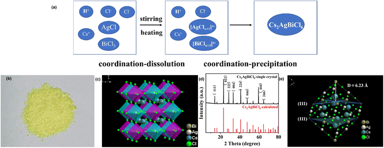
Therefore, we prepared Cs2AgBiCl6-DP SCs by coordination–dissolution (as shown in eqn (1) and (2)) and coordination–precipitation (as shown in eqn (3)). The reaction schematic for coordination–dissolution and coordination–precipitation is shown in Fig. 1a. The photograph of the prepared Cs2AgBiCl6-DP SCs is shown in Fig. 1b. The color of Cs2AgBiCl6-DP SCs is yellow. The three-dimensional crystal structure of Cs2AgBiCl6 was analyzed through a series of operations (collecting X-ray diffraction intensity data, identifying heavy atoms through direct method, and then refining). The three-dimensional crystal structure of Cs2AgBiCl6-DP SCs is shown in Fig. 1c, a cubic crystal system with space group Fm![[3 with combining macron]](https://www.rsc.org/images/entities/char_0033_0304.gif) m (225). The unit cell dimensions are as follows: a = 10.7930(8) Å, α = 90°; b = 10.7930(8) Å, β = 90°; c = 10.7930(8) Å, γ = 90°. Cubic Cs2AgBiCl6 is composed of alternating [AgCl6]5− and [BiCl6]3− octahedral units, with the central position occupied by Cs+. Bi3+ and Ag+ are located at the centres of the octahedra [BiCl6]3− and [AgCl6]5− respectively, and six Cl− are located at the six corners of the octahedron. Detailed crystallographic information is given in Tables 1 and S1–S3.† CCDC 2385937 (Cs2AgBiCl6) includes the ESI† crystallographic data for this work. This data is provided by the Cambridge Crystallographic Data Centre and the Karlsruhe Information Center and is available for free at http://www.ccdc.cam.ac.uk/structures. Similar structures have been described in the literature.19,20
m (225). The unit cell dimensions are as follows: a = 10.7930(8) Å, α = 90°; b = 10.7930(8) Å, β = 90°; c = 10.7930(8) Å, γ = 90°. Cubic Cs2AgBiCl6 is composed of alternating [AgCl6]5− and [BiCl6]3− octahedral units, with the central position occupied by Cs+. Bi3+ and Ag+ are located at the centres of the octahedra [BiCl6]3− and [AgCl6]5− respectively, and six Cl− are located at the six corners of the octahedron. Detailed crystallographic information is given in Tables 1 and S1–S3.† CCDC 2385937 (Cs2AgBiCl6) includes the ESI† crystallographic data for this work. This data is provided by the Cambridge Crystallographic Data Centre and the Karlsruhe Information Center and is available for free at http://www.ccdc.cam.ac.uk/structures. Similar structures have been described in the literature.19,20
| Empirical formula | Cs2AgBiCl6 |
| Formula weight | 795.37 |
| Temperature | 298(2) K |
| Wavelength | 0.71073 Å |
| Crystal system | Cubic |
| Space group (no.) | Fm![[3 with combining macron]](https://www.rsc.org/images/entities/char_0033_0304.gif) m (225) m (225) |
| Unit cell dimensions | a = 10.7930(8) Å, α = 90° |
| b = 10.7930(8) Å, β = 90° | |
| c = 10.7930(8) Å, γ = 90° | |
| V/Å3 | 1257.26(16) |
| Z | 4 |
| ρcalcd/mg m−3 | 4.202 |
| Absorption coefficient/mm−1 | 22.458 |
| F(000) | 1368 |
| Crystal size/mm3 | 0.20 × 0.19 × 0.13 |
| Theta range for data collection | 3.27 to 24.94° |
| Limiting indices | 0 ≤ h ≤ 7, 0 ≤ k ≤ 9, 1 ≤ l ≤ 12 |
| Reflections collected/unique | 83/83 [R(int) = 0.0000] |
| Data/restraints/parameters | 83/0/8 |
| Goodness-of-fit on F2 | 1.161 |
| Final R indices [I > 2σ(I)] | R1 = 0.1119, wR2 = 0.2493 |
| R Indices (all data) | R1 = 0.1557, wR2 = 0.2716 |
| Largest diff. peak and hole/e Å−3 | 3.218 and −4.198 |
As shown in Fig. 1d, we compared the powder X-ray diffraction (PXRD) pattern of the experimental crystal powder with those calculated by single crystal information data with Diamond software. By comparison, it can be found that the diffraction peaks obtained by the two methods are basically consistent. The diffraction peaks at 23.3, 33.2 and 47.4° are for the (220), (004) and (224) crystal planes, respectively. According to Bragg's Law (4), the distance between the (111) crystal plane corresponding to 16.23° is calculated to be 6.23 Å.
2d![[thin space (1/6-em)]](https://www.rsc.org/images/entities/char_2009.gif) sin sin![[thin space (1/6-em)]](https://www.rsc.org/images/entities/char_2009.gif) θ = nλ θ = nλ
| (4) |
3.2 SEM, EDS, element mapping of Cs2AgBiCl6-DP SCs
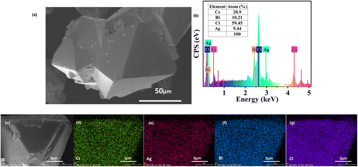
The morphology of Cs2AgBiCl6-DP SCs is displayed using SEM, as shown in Fig. 2a. The crystal shape tends to grow into an octahedron. The size of the crystal is approximately 100 μm. To further verify the composition and proportion of the Cs2AgBiCl6-DP SCs, EDS testing was conducted. According to the peak positions and the peak areas in the EDS spectrum, an elemental composition and proportion table is shown in Fig. 2b. Cs, Ag, Bi, and Cl elements with an atomic ratio of approximately 2![[thin space (1/6-em)]](https://www.rsc.org/images/entities/char_2009.gif) :
:![[thin space (1/6-em)]](https://www.rsc.org/images/entities/char_2009.gif) 1
1![[thin space (1/6-em)]](https://www.rsc.org/images/entities/char_2009.gif) :
:![[thin space (1/6-em)]](https://www.rsc.org/images/entities/char_2009.gif) 1
1![[thin space (1/6-em)]](https://www.rsc.org/images/entities/char_2009.gif) :
:![[thin space (1/6-em)]](https://www.rsc.org/images/entities/char_2009.gif) 6 are consistent with that expected of Cs2AgBiCl6-DP SCs. It is evident that the elements of Cs, Ag, Bi, and Cl are uniformly distributed in Cs2AgBiCl6 DP SCs, as shown in Fig. 2d–g, respectively.
6 are consistent with that expected of Cs2AgBiCl6-DP SCs. It is evident that the elements of Cs, Ag, Bi, and Cl are uniformly distributed in Cs2AgBiCl6 DP SCs, as shown in Fig. 2d–g, respectively.
3.3 Band gap and luminescence of Cs2AgBiCl6-DP SCs
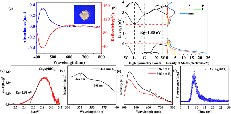
The photograph of Cs2AgBiCl6-DP SCs under a 365 nm ultraviolet lamp is shown in Fig. 3a. Compared to Fig. 1a, the crystal appears bright yellow under 365 nm ultraviolet light irradiation. The UV-visible (UV-vis) absorption and diffuse reflectance spectra of Cs2AgBiCl6-DP SCs are shown in Fig. 3a. The absorption peak is observed at 436 nm. The absorption spectrum cuts off at 540 nm. The trend of the reflectance spectra is, as expected, opposite to that of the absorption spectra. The bandgap and density of states calculated theoretically are shown in Fig. 3b. According to whether the positions of the conduction band bottom and valence band top in the K-space of a semiconductor are consistent, its bandgap can be divided into direct bandgap and indirect bandgap. It can be observed that the positions of the conduction band bottom and valence band top of the crystal are not consistent in K-space, which indicates that Cs2AgBiCl6-DP SCs has an indirect band gap. The theoretically calculated bandgap is 1.85 eV. Meanwhile, the band gap of Cs2AgBiCl6-DP SCs was calculated from the UV-vis spectrum using a Tauc plot. The hν–(hνF[R∞])2 curve of Cs2AgBiCl6-DP SCs is shown in Fig. 3c. Its band gap is extrapolated to be 2.51 eV. Compared with the theoretically calculated bandgap, it is larger. According to the excitation spectrum in Fig. 3d, there are two excitation peaks at 326 and 365 nm for 444 nm emission. The luminescence spectra with excitation wavelengths of 326 and 365 nm are shown in Fig. 3e. There are four fluorescence peaks located at 443, 615, 650 and 723 nm. The intensity of the fluorescence peak excited by 326 nm is stronger than that excited by 365 nm. To understand the lifetime of photogenerated charge carriers and internal defects of Cs2AgBiCl6-DP SCs, fluorescence lifetime testing was conducted and the results are shown in Fig. 3f. The fluorescence lifetime of the compound is approximately 4.16 ns from fitting the curve. The short fluorescence lifetime may be due to internal defects, which could affect the photoelectric performance.3.4 XPS and EPR analysis of Cs2AgBiCl6-DP SCs
XPS was performed on Cs2AgBiCl6-DP SCs, and the results are shown in Fig. 4a. Fig. 4b–e show the fine scan XPS orbital energy spectra of Cs 3d, Ag 3d, Bi 4f, and Cl 2p for Cs2AgBiCl6-DP SCs, respectively. The peak positions of electron binding energies at 724.4 and 738.3 eV are attributed to the Cs+ 3d5/2 and 3d3/2 orbitals, respectively; those at 368 and 374 eV are attributed to the Ag+ 3d5/2 and 3d3/2 orbitals, respectively; those at 159.1 and 164.4 eV are attributed to the Bi3+ 4f7/2 and 4f5/2 orbitals, respectively; and those at 198.1 and 199.7 eV originate from the Cl− 2p3/2 and 2p1/2 orbitals, respectively. EPR testing was also performed, and the results are shown in Fig. 4f, indicating the existence of a single electron in Cs2AgBiCl6-DP.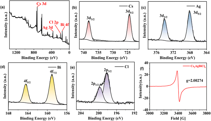 | ||
| Fig. 4 (a) XPS full spectrum of Cs2AgBiCl6-DP SCs; XPS characterization of Cs 3d (b), Ag 3d (c), Bi 4f (d) and Cl 2p (e) in Cs2AgBiCl6-DP SCs; (f) EPR curve of Cs2AgBiCl6-DP SCs. | ||
3.5 The preparation process, SEM, EDS and element mapping of Cs2AgBiCl6-DP thin film
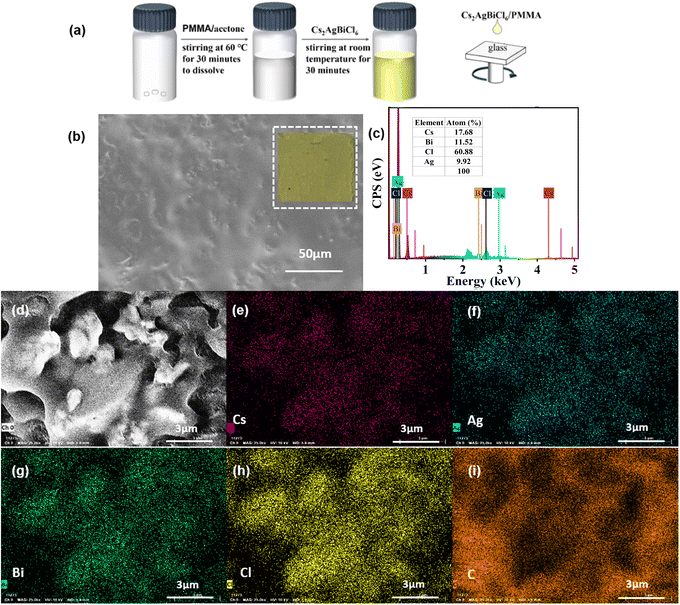
If a crystalline material can be made into a high-quality thin film, it can be applied in many fields. However, Cs2AgBiCl6-DP SCs is difficult to form into a thin film due to the insolubility of inorganic materials. We have attempted and designed several methods (temperature optimization, solvent screening, etc.), but none of them produced a good thin film of Cs2AgBiCl6-DP. Herein, we prepared Cs2AgBiCl6/PMMA thin film by spin coating a suspension of Cs2AgBiCl6 DP and PMMA (the mass ratio of PMMA to Cs2AgBiCl6-DP is 1![[thin space (1/6-em)]](https://www.rsc.org/images/entities/char_2009.gif) :
:![[thin space (1/6-em)]](https://www.rsc.org/images/entities/char_2009.gif) 4) in acetone solvent. The preparation process of spin coated Cs2AgBiCl6-DP thin film on glass is shown in Fig. 5a.
4) in acetone solvent. The preparation process of spin coated Cs2AgBiCl6-DP thin film on glass is shown in Fig. 5a.
The morphology of Cs2AgBiCl6-DP thin film was imaged using SEM, as shown in Fig. 5b. Some Cs2AgBiCl6-DP particles were observed. To further verify the composition and proportion of the Cs2AgBiCl6-DP thin film, EDS testing was conducted. According to the EDS spectrum in Fig. 5c, the sample is composed of Cs, Ag, Bi, and Cl elements with an atomic ratio of approximately 2![[thin space (1/6-em)]](https://www.rsc.org/images/entities/char_2009.gif) :
:![[thin space (1/6-em)]](https://www.rsc.org/images/entities/char_2009.gif) 1
1![[thin space (1/6-em)]](https://www.rsc.org/images/entities/char_2009.gif) :
:![[thin space (1/6-em)]](https://www.rsc.org/images/entities/char_2009.gif) 1
1![[thin space (1/6-em)]](https://www.rsc.org/images/entities/char_2009.gif) :
:![[thin space (1/6-em)]](https://www.rsc.org/images/entities/char_2009.gif) 6, further confirming the chemical composition of the Cs2AgBiCl6-DP thin film, which is consistent with the previous analysis of the Cs2AgBiCl6-DP SCs. Through the element mapping images of Cs, Ag, Bi, Cl, and C in the Cs2AgBiCl6-DP film (from Fig. 5d–i), it is evident that the elements of Cs, Ag, Bi, and Cl are uniformly and tightly distributed in the Cs2AgBiCl6-DP particles.
6, further confirming the chemical composition of the Cs2AgBiCl6-DP thin film, which is consistent with the previous analysis of the Cs2AgBiCl6-DP SCs. Through the element mapping images of Cs, Ag, Bi, Cl, and C in the Cs2AgBiCl6-DP film (from Fig. 5d–i), it is evident that the elements of Cs, Ag, Bi, and Cl are uniformly and tightly distributed in the Cs2AgBiCl6-DP particles.
3.6 Photoluminescence of Cs2AgBiCl6-DP thin film
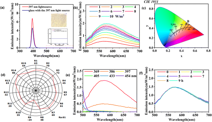
As shown in Fig. 6a, it can be observed that the Cs2AgBiCl6-DP thin film emits significant light under 365 nm illumination. Based on the luminescence characteristics of Cs2AgBiCl6-DP thin film, the photoluminescence intensity of the thin film was measured using a 350 multifunctional spectrometer, using the glass without Cs2AgBiCl6-DP thin film as reference. No emission peaks between 500 and 700 nm are observed for the ultra-flat glass without Cs2AgBiCl6-DP thin film, as shown in Fig. 6a. In contrast, a new emission peak between 500 and 700 nm is observed for the ultra-flat glass with Cs2AgBiCl6-DP thin film, as shown in Fig. 6b. The dependence relationship between emission intensity (500 to 700 nm) and different light intensities (1 to 10 W m−2) of 369 nm was studied. As shown in Fig. 6b, the intensity of the emission peak increases with the increase of light intensity at 369 nm. A chromaticity diagram was plotted based on the emission intensity of Cs2AgBiCl6 DP thin film at 369 nm with 10 W m−2, as shown in Fig. 6d. The red, green, and blue primary stimulus values of Cs2AgBiCl6 DP thin film are 150.155, 158.090, and 9.353, respectively. The chromaticity coordinates of Cs2AgBiCl6 DP thin film are as follows: x = 0.4727, y = 0.4977, z = 0.02944. According to the color temperature classification in Fig. 6c, the color temperature of Cs2AgBiCl6-DP thin film is greater than 3000 K, which belongs to the medium color temperature category. The detailed color rendering index of the thin film was obtained through emission spectroscopy, with a Ra of 61, as shown in Fig. 6d. The effect of different wavelengths (369, 386, 397, 405, 433, and 454 nm) on emission peak was investigated. The intensity of the emission peak decreases with increasing wavelength at 10 W m−2, as shown in Fig. 6e. In addition, stability testing of the photoluminescence was conducted. The emission intensity remains basically unchanged under continuous illumination for 9 hours at 369 nm at 5 W m−2, as shown in Fig. 6f. This indicates that the Cs2AgBiCl6-DP thin film has good stability.3.7 Resistivity properties of Cs2AgBiCl6-DP thin film
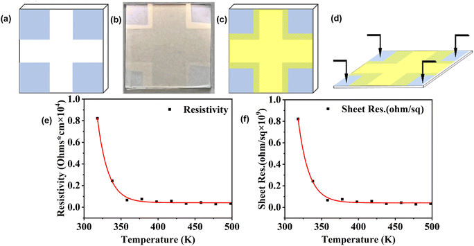
To study the resistivity characteristics of Cs2AgBiCl6 DP thin film, we used a four-probe method to measure the resistance of the thin film as a function of temperature. The schematic diagrams of the layout of the conductive glass substrate are shown in Fig. 7a. The small squares at the four corners are conductive areas used to contact the four probes. A photograph of the evaporated Cs2AgBiCl6 DP thin film on conductive glass is shown in Fig. 7b. The SEM image of the cross-sectional morphology of the Cs2AgBiCl6-DP film is shown in Fig. S1.† Its thickness is approximately 100 nm. The SEM and EDS of Cs2AgBiCl6 DP thin film deposited by evaporation are shown in Fig. S1.† It can be observed that the thin film clearly covers the edges of the conductive area. The schematic diagram after evaporation is shown in Fig. 7c. The schematic diagram of the four probe test is shown in Fig. 7d. The variation of resistivity with temperature was tested on the thin film. The resistivity formula is shown as formula (5).
 | (5) |
According to above formula, the results obtained by the four-probe method indicate that the resistance gradually decreases as the temperature increases (from 298 to 498 K). Fitting the data reveals a negative exponential relationship between resistivity and temperature, as shown in Fig. 7e.
The formula for square resistance is shown in formula (6).
 | (6) |
The square resistance gradually decreases with decreasing temperature, as shown in Fig. 7f. By fitting the data of square resistance at different temperatures, it is found that the variation of square resistance with temperature follows a negative exponential relationship, as shown in Fig. 7f.
4 Conclusion
In this study, we prepared Cs2AgBiCl6 DP SCs by coordination–dissolution and coordination–precipitation and prepared thin films by a two-step method of nanomaterialization-polymer bonding. Cs2AgBiCl6 DP SCs have photoluminescent properties, but the performance is not very ideal. The next step can be improvement by mixing rare elements. Based on the results of the resistivity, it can be inferred that this material has a promising application in the field of thermal sensitivity. These results can provide some ideas and prospects for the research and development of lead-free double perovskite materials in the field of optoelectronics in the future.Data availability
The data that support the findings of this study are available from the corresponding authors upon reasonable request.Conflicts of interest
There are no conflicts to declare.Acknowledgements
Thanks to Xuewei Fu for providing the crystals and crystal data.Notes and references
- M. R. Filip, G. E. Eperon, H. J. Snaith and F. Giustino, Nat. Commun., 2014, 5, 5757 CrossRef CAS PubMed.
- S. De Wolf, J. Holovsky, S. J. Moon, P. Löper, B. Niesen, M. Ledinsky, F. J. Haug, J. H. Yum and C. Ballif, J. Phys. Chem. Lett., 2014, 5, 1035–1039 CrossRef CAS PubMed.
- X. Chen, H. Lu, K. Wang, Y. Zhai, V. Lunin, P. C. Sercel and M. C. Beard, J. Am. Chem. Soc., 2021, 143, 19438–19445 CrossRef CAS PubMed.
- C. C. Stoumpos, C. D. Malliakas and M. G. Kanatzidis, Inorg. Chem., 2013, 52, 9019–9038 CrossRef CAS PubMed.
- S. D. Stranks, G. E. Eperon, G. Grancini, C. Menelaou, M. J. P. Alcocer, T. Leijtens, L. M. Herz, A. Petrozza and H. J. Snaith, Science, 2013, 342, 341–344 CrossRef CAS PubMed.
- J. Y. Kim, J.-W. Lee, H. S. Jung, H. Shin and N.-G. Park, Chem. Rev., 2020, 120, 7867–7918 CrossRef CAS PubMed.
- J. X. Ding, S. J. Du, Z. Y. Zuo, Y. Zhao, H. Z. Cui and X. Y. Zhan, J. Phys. Chem. C, 2017, 121, 4917–4923 CrossRef CAS.
- W. D. Xu, Q. Hu, S. Bai, C. X. Bao, Y. F. Miao, Z. C. Yuan, T. Borzda, A. J. Barker, E. Tyukalova, Z. J. Hu, M. Kawecki, H. Y. Wang, Z. B. Yan, X. J. Liu, X. B. Shi, K. Uvdal, M. Fahlman, W. J. Zhang, M. Duchamp, J. M. Liu, A. Petrozza, J. P. Wang, L. M. Liu, W. Huang and F. Gao, Nat. Photonics, 2019, 13, 418–419 CrossRef CAS.
- M. Y. Hu, G. P. Wang, Q. H. Zhang, J. Gong, Z. Xing, J. Q. Gao, J. Wang, P. Zeng, S. Z. Zheng, M. Z. Liu, Y. Y. Zhou and S. H. Yang, J. Energy Chem., 2022, 72, 487–494 CrossRef CAS.
- M. Li, F. M. Li, J. Gong, T. K. Zhang, F. Gao, W. H. Zhang and M. Z. Liu, Small Struct., 2022, 3, 100102 Search PubMed.
- M. Ren, X. Qian, Y. Chen, T. Wang and Y. Zhao, J. Hazard. Mater., 2022, 426, 127848 CrossRef CAS PubMed.
- S. Ahmed, F. Jannat, M. A. K. Khan and M. A. Alim, Optik, 2021, 225, 165765 CrossRef CAS.
- S. D. Yang, W. F. Fu, Z. Q. Zhang, H. Z. Chen and C. Z. Li, J. Mater. Chem. A, 2017, 5, 11462–11482 RSC.
- G. Volonakis, M. R. Filip, A. A. Haghighirad, N. Sakai, B. Wenger, H. J. Snaith and F. Giustino, J. Phys. Chem. Lett., 2016, 7, 1254–1259 CrossRef CAS PubMed.
- M. R. Filip, S. Hillman, A. A. Haghighirad, H. J. Snaith and F. Giustino, J. Phys. Chem. Lett., 2016, 7, 2579–2585 CrossRef CAS PubMed.
- N. Chen, T. Cai, W. Li, K. Hills-Kimball, H. Yang, M. Que, Y. Nagaoka, Z. Liu, D. Yang, A. Dong, C.-Y. Xu, R. Zia and O. Chen, ACS Appl. Mater. Interfaces, 2019, 11, 16855–16863 CrossRef CAS PubMed.
- M. Li, H. Zhou, J. Yin and X. Zhang, J. Mater. Chem. C, 2023, 12, 154–160 RSC.
- X. Wang, M. Li, W. Cao, W. Li, H. Gao, Q. Zhang, H. Zhou and X. Zhang, Appl. Organomet. Chem., 2023, 37, e7245 CrossRef CAS.
- M. Jeevaraj, D. Sivaganesh, S. Saravanakumar, S. A. Bahadur, S. Sudhahar and M. K. Kumar, Opt. Mater., 2023, 143, 114294 CrossRef CAS.
- E. T. McClure, M. R. Ball, W. Windl and P. M. Woodward, Chem. Mater., 2016, 28, 1348–1354 CrossRef CAS.
Footnote |
| † Electronic supplementary information (ESI) available. CCDC 2385937. For ESI and crystallographic data in CIF or other electronic format see DOI: https://doi.org/10.1039/d4ra06936f |
| This journal is © The Royal Society of Chemistry 2024 |

