DOI:
10.1039/D4RA07912D
(Paper)
RSC Adv., 2024,
14, 36675-36697
Evaluation of design and device parameters for lead-free Sr3PBr3/Sr3NCl3 duel-layer perovskite photovoltaic device technology
Received
6th November 2024
, Accepted 12th November 2024
First published on 18th November 2024
Abstract
The study looks into how Sr3PBr3 and Sr3NCl3 double perovskite materials can be used as absorbers in perovskite solar cells (PSCs). Computational Sr3PBr3 and Sr3NCl3 simulations were employed to assess the performance of each absorber together with electron transport layers (ETL), with a particular emphasis on optimizing ETL thickness to improve charge transport and synchronize current outputs. The simulations yielded valuable insights into the electronic and optical characteristics of the individual absorbers. Subsequently, a tandem simulation was performed to adjust each layer's thickness, ensuring that both devices' current outputs were aligned for maximum system efficiency. The findings revealed that the tandem configuration of Sr3PBr3 and Sr3NCl3 surpassed the performance of the individual absorber setups, attributed to the optimized ETL thicknesses that enhanced charge transport and facilitated effective current matching. This study makes a significant contribution to the design and optimization of tandem PSCs utilizing Sr3PBr3 and Sr3NCl3 absorbers, paving the way for improved overall device efficiency. We investigated three device configurations to find the optimum structure. FTO/SnS2/Sr3PBr3/Ni, FTO/SnS2/Sr3NCl3/Ni, and FTO/SnS2/Sr3PBr3/Sr3NCl3/Ni are considered as Device-I, II, and III. In Device-I, the execution parameters are power conversion efficiency (PCE) of 24.26%, an open-circuit voltage (VOC) of 1.23 V, a short-circuit current density (JSC) of 24.65 mA cm−2, and a fill factor (FF) of 87.42%. For Device-II, PCE, FF, VOC, and JSC are correspondingly 20.35%, 87.91%, 1.28 V, and 18.07 mA cm−2. The further refined tandem configuration achieved a PCE of 30.32%, with a VOC of 1.27 V, an FF of 90.14%, and a JSC of 26.44 mA cm−2, demonstrating the potential of this methodology in enhancing PSC performance.
1. Introduction
The need for energy worldwide is steadily increasing, driven by an expanding population, which raises concerns about the exhaustion of nonrenewable supplies and the associated ecological consequences. This situation has catalyzed a shift towards renewable energy sources, with solar energy standing out as a prominent choice due to its plentiful, clean, and limitless characteristics.1 The adoption of solar energy not only mitigates environmental challenges but also fosters sustainable energy solutions, such as solar architecture,2 solar heating,3 photovoltaics,4 and photocatalytic water-splitting technologies.5,6 Among these, photovoltaics has attracted considerable interest because of their ability to use the PV effect to turn sunlight into energy. Solar cells (SCs), which are essential components of photovoltaics, capture sunlight to generate electricity and can be divided into three generations. The first generation is based on wafer technology; the second generation utilizes thin films; and the third generation features organic materials. Although first- and second-generation SCs have historically led the market, their high production costs, intricate manufacturing processes, and environmental concerns have limited their widespread use. Researchers are diligently investigating new materials for solar cells (SCs) that prioritize both cost-effectiveness and environmental sustainability. A variety of SC types have been created, including polycrystalline and single-crystalline silicon SCs,7 copper indium gallium selenide (CIGS) SCs,8 cadmium telluride (CdTe) SCs,9 quantum dot SCs,10 organic SCs,11 and perovskite solar cells (PSCs),12 each presenting unique benefits. In the commercialization process of SCs, PCE and material costs are critical considerations. Currently, third-generation silicon-based SCs dominate the market, achieving impressive PCEs of approximately 25–26%.13 However, innovative third-generation PSCs are emerging as formidable alternatives to conventional silicon SCs, boasting remarkable PCEs of up to 22.1%.14,15 To further improve efficiency, researchers are utilizing various strategies, including structural and compositional engineering, optimizing ETLs and HTLs, and investigating double and graded absorber configurations in PSCs.16–19 The Sr3PBr3 and Sr3NCl3 structure, characterized by the substitution of P (phosphorus) and N (nitrogen) for lead, is recognized as one of the most encouraging configurations due to its superior crystalline nature, extended carrier duration, and enhanced stability in comparison to lead-based perovskites.20,21 Double perovskite compounds present considerable advantages over their single perovskite counterparts across various applications. Notable benefits of double perovskites include increased stability, as the incorporation of two different cations in the A-site of the crystal lattice bolsters structural integrity and resistance to degradation, making them more suitable for prolonged device operation.22 Furthermore, double perovskites facilitate property tuning through the modification of cation combinations at the A-site, allowing for precise control over bandgap, electronic structure, and photosensitivity, thus enabling customization to fulfill specific application requirements.23 Double perovskite materials present a wider absorption spectrum compared to single perovskites, primarily due to the presence of multiple cations. This diversity can lead to an increased bandgap, enabling the absorption of a broader range of solar photons. As a result, the enhanced absorption improves the utilization of sunlight, which in turn boosts photocurrent generation and elevates power conversion efficiency. Furthermore, double perovskites typically demonstrate reduced carrier recombination rates. The incorporation of various cations helps to optimize energy-level alignments, thereby minimizing nonradiative recombination and prolonging the lifetimes of charge carriers.24–26 To optimize the performance of double-layer perovskite materials like Sr3PBr3 and Sr3NCl3 in solar cells, composition tuning and improving crystallinity through advanced deposition methods are crucial. Selecting a suitable electron transport layer (ETL) with high electron mobility is essential for efficient charge extraction, and optimizing the ETL thickness can help balance electron collection and recombination losses. Implementing a double-layer architecture can enhance charge separation by minimizing energy barriers at the interfaces. Incorporating light-trapping techniques and optical coatings can significantly boost light absorption and overall efficiency. Effective encapsulation protects the perovskite layer from moisture, improving device longevity. Exploring tandem configurations that combine perovskite layers with other materials can maximize energy harvesting across a broader spectrum. Finally, using computer simulations to model device performance can guide material and structural optimizations for improved efficiency. These materials also exhibit excellent charge transport characteristics, attributed to their unique crystal structures and the deliberate inclusion of different cations, which enhance charge carrier mobility and promote effective charge extraction. These features render double perovskites particularly appealing for application in diodes that produce light, solar cells, and photosensors, as they provide improved stability, adjustable properties, expanded absorption capabilities, decreased recombination rates, and enhanced charge transport, all of which contribute to the advancement of more efficient and stable optoelectronic devices. The ETL, characterized as n-type, is essential for influencing the JSC and VOC in photovoltaic devices. The VOC is notably affected by the alignment of the band at the junction of the absorber and backstop layers. This alignment, named the conduction band offset (CBO), can be classified into three types: cliff, plane, or spike. A spike at the interface is beneficial as it minimizes recombination losses, while a cliff alignment decreases in VOC. To ensure efficient transmission of electrons between the ETL and the absorber, thereby maintaining the fill factor and density of current, the height of the spike should be kept to a minimum. Tin sulfide (SnS2) is chosen for the ETL in this solar cell because of its advantageous electrical properties, including a band gap of approximately 2.24 eV, which positions it as an effective ETL material. SnS2 is recognized for its low absorption losses, high electron mobility, and good visibility spectrum transparency. The way its conduction band aligns with absorber materials like Sr3PBr3 facilitates efficient electron extraction and inhibits hole back-transfer. Furthermore, SnS2 establishes stable interfaces with the FTO foundation; this reduces the losses from interface recombination and increases adhesion. Its chemical stability and ease of fabrication further confirm its appropriateness for solar energy applications. In the structure, the absence of a hole transport layer (HTL) could be a deliberate design decision based on the favorable alignment of energy levels between the materials. This alignment allows for efficient hole extraction directly to the Ni electrode, eliminating the need for a dedicated HTL. Such an approach simplifies the device architecture, reducing fabrication complexity and minimizing potential interface losses that might occur with an additional layer. If the electron transport layer (SnS2) effectively facilitates electron extraction and the absorber materials (Sr3PBr3 and Sr3NCl3) demonstrate good hole transport properties, the overall performance could remain high without an HTL. This design choice would be further justified by evidence of minimal recombination and optimal band alignment, ensuring efficient charge separation and collection. By leveraging the inherent properties of the materials involved, the device can maintain high efficiency while reducing manufacturing challenges. Ultimately, this streamlined structure could lead to better performance and reliability in practical applications. Thus, the decision to forgo an HTL appears strategically sound, balancing simplicity with effective charge transport. Following the deposition of SnS2 via pulsed laser deposition (PLD), the layers were subjected to optical and electrical analysis to evaluate critical attributes like bandgap, concentration of carrier, and electron affinity. The incorporation of dual absorber layers in PSCs is primarily intended to enhance light absorption capabilities and establish a hybrid cell architecture.
This study focuses on a specific PSC design that features Sr3PBr3/Sr3NCl3, which hasn't been looked into before. We utilize SCAPS-1D software to serve as a model for this novel PSC configuration with a cross-link. In our design, the dual-absorber solar cell comprises Sr3PBr3 as the upper absorber and Sr3NCl3 as the lower absorber. The SCAPS-1D model presumes ideal tunneling connections between the two absorbers, eliminating any visual or electrical losses. The execution of the simulation is affected by various factors, including the absorber's thickness layers, doping concentrations, and defect densities. We conduct a comprehensive analysis of these parameters to evaluate their impact on the model's electrical properties. Furthermore, we investigate how variations in shunt resistance, temperature, series resistance, and the electrode for the back contact influence the electrical performance of the Sr3PBr3/Sr3NCl3-based PSC model. For electron transport within the simulation, SnS2 is chosen as the material.
2. Methods for building devices and simulating them
2.1 Design of the apparatus
In this research on PSCs, a substrate made of FTO glass was used, with SnS2 functioning as the ETL and nickel (Ni) serving as the electrode. The light absorption layer consisted of either Sr3PBr3, Sr3NCl3, or a bilayer heterojunction that combined both Sr3PBr3 and Sr3NCl3. The structures and band alignment of these three PSC types are illustrated in Fig. 1(a–f). Both configurations for the dual-absorber solar cell under consideration are represented as FTO/SnS2/Sr3PBr3/Sr3NCl3/Ni, as displayed in Fig. 1(e and f). When the positions of the absorber layers in Device-III are switched to FTO/SnS2/double absorber (Sr3PBr3, Sr3NCl3)/Ni, the device's functionality increases, yielding a PCE, VOC, FF, and JSC of 30.32%, 1.27 V, 90.14%, and 26.44 mA cm−2. Every simulation was run with regular operating parameters: 300 K in temperature, a frequency of 106 Hz, and standard AM1.5G1 solar illumination. While existing literature data was utilized to optimize the properties of other layers, simulations were performed to determine the ideal thickness of the layer that absorbs. This company assures that there will be no optic loss or electrical interference in the tunnel connecting the two absorbers. To minimize shifting and protect the uppermost layers from exposure to solvent and harm when sputtering, the dual-absorber solar cells have a contoured recombination layer sandwiched between the absorber layers. Drawing from relevant computational and experimental studies from the body of existing literature, Table 1 lists the electrical parameters used in the simulations. The parameters include layer thickness (t), mobilities for electrons and holes (mn & mp), relative dielectric constant (εr), bandgap (Eg), electron affinity (χ), thermal velocities (vte, vtp), effective state densities for the bands of valence and conduction (Nv & Nc), overall defect concentration (Nt), and donor and acceptor concentrations (ND & NA). Conversely, the interface properties are displayed in Table 2 for the SnS2/Sr3PBr3, SnS2/Sr3NCl3, and Sr3PBr3/Sr3NCl3 systems, highlighting the impact of flaw concentration at the interfaces while maintaining a constant overall defect density.
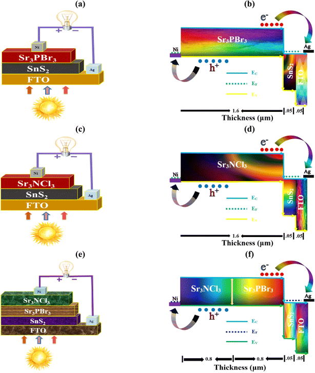 |
| | Fig. 1 Diagrammatic and band alignment designs set up of (a and b) Device-I, (c and d) Device-II, and (e and f) Device-III. | |
Table 1 An overview of the dual absorber, ETL, and FTO layer settings selected for the SCAPS-1D simulation
| Parameters |
FTO27–30 |
SnS2 (ref. 31) |
Sr3PBr3 (ref. 20) |
Sr3NCl3 (ref. 21) |
| Layer thickness, t (nm) |
50 |
50 |
800 |
800 |
| Band gap, Eg (eV) |
3.6 |
3.6 |
1.528 |
1.75 |
| Electron affinity, χ (eV) |
4.5 |
4.24 |
4.16 |
3.97 |
| Dielectric permittivity (relative, ∈r) |
10 |
10 |
5.28 |
4.95 |
| CB effective density of states, NC (cm−3) |
2 ×10¹⁸ |
2.2 ×10¹⁸ |
1.18× 10¹⁸ |
8.228× 10¹⁸ |
| VB effective density of states, NV (cm−3) |
1.8 ×10¹⁹ |
1.8 ×10¹⁹ |
1.66× 10¹⁹ |
1.14× 10¹⁹ |
| Electron mobility, μn (cm2 V−1 s−1) |
100 |
50 |
25 |
50 |
| Hole mobility, μh (cm2 V−1 s−1) |
20 |
50 |
20 |
50 |
| Donor density, ND (cm−3) |
1018 |
1017 |
0 |
0 |
| Acceptor density, NA (cm−3) |
0 |
0 |
1017 |
1017 |
| Defect density, Nt (cm−3) |
1014 |
1014 |
1012 |
1012 |
Table 2 Interface characteristics employed in solar cells featuring heterojunctions, including FTO/SnS2/(Sr3PBr3, Sr3NCl3)/Ni structures
| Interface |
Reference for defect energy level |
Energetic distribution |
Defect position above the highest Ev (eV) |
Defect type |
Capture cross-section: electrons/holes (cm2) |
Total defect density (cm−2) |
| Sr3PBr3/SnS2 |
Above the highest Ev |
Single |
0.06 |
Neutral |
1 × 10 −19 |
1.0 × 10¹⁰ |
| Sr3NCl3/SnS2 |
Above the highest Ev |
Single |
0.06 |
Neutral |
1 × 10 −19 |
1.0 × 10¹⁰ |
| Sr3NCl3/Sr3PBr3 |
Above the highest Ev |
Single |
0.06 |
Neutral |
1 × 10 −19 |
1.0 × 10¹⁰ |
| Sr3PBr3/SnS2 |
Above the highest Ev |
Single |
0.06 |
Neutral |
1 × 10 −19 |
1.0 × 10¹⁰ |
2.2 Methods of simulation
A sophisticated software program called SCAPS-1D (version 3.3.0.7) was created to simulate solar cells, concentrating on the examination of each layer's characteristics inside these cells.32 Created by Marc Burgelman at the Department of Electronics and Information Systems at the University of Gent in Belgium, this program is extensively utilized for the evaluation of various types of SCs.33,34 It provides the photovoltaic research community with in-depth information on critical parameters, including PCE, VOC, FF, and JSC for each layer. The software accomplishes these analyses by solving three fundamental equations: the equations for charge transport (eqn (4) and (5)), continuity (eqn (2) and (3)), and Poisson (eqn (1)), which characterize the motion of charge carriers:35,36| |
 | (1) |
E(x) denotes the electrostatic potential in this context, while the symbol for an electron's charge is e. The relative permittivity (εr) and vacuum permittivity (ε0) are denoted by these symbols, respectively. In addition, the quantity between electrons and holes is indicated by n(x) and p(x), respectively. ρn and ρp show the electron and hole distributions, respectively, whereas ND and NA symbolize the charge concentrations of donors and recipients, respectively.| |
 | (2) |
| |
 | (3) |
Here, Jn and Jp signify the prevailing density of electrons and holes, whereas R and G stand for the rearranging of molecules and generation rates, respectively. Eqn (4) and (5) show how drift and diffusion lead to carrier transport in semiconductors.| |
 | (4) |
| |
 | (5) |
In this case, electrons and holes have different diffusion coefficients represented by Dn and Dp, respectively, while the electron and hole mobilities are denoted by εn and εp. Furthermore, the analytical mathematical formula for the absorption rate is specified as in eqn (6):37| |
 | (6) |
Here, hν represents photon energy and Bα is a steady coefficient given as 105 cm−1 eV−0.5. Eqn (7) and (8) illustrate the relationship between key PV characteristics, providing a mathematical framework that demonstrates how these critical parameters interact within the solar cell structure. These equations help in being aware of how different elements affect the overall performance of PV devices, offering valuable insights for optimizing solar cell efficiency.38| |
 | (7) |
| |
 | (8) |
In these equations, Pin signifies the solar energy input, while Pmax indicates the highest possible power output.
3. Result and discussion
3.1 Relationship between the left contact work function and solar cell efficiency
The effectiveness and overall execution of solar panels are enormously affected by the left contact, which is vital for cellular efficiency.39 To optimize performance, the left contacts, an integral part of the electrical system that facilitates current extraction, should exhibit minimal resistive losses. Inadequate contact design can lead to heightened resistance in series, which diminishes the output of electricity and flow of current. Furthermore, the left contact must provide robust adherence and limited mixture interaction using the semiconductor to ensure stability and longevity. Suboptimal contact designs can result in shading, decreased light absorption, and a reduced active area. Well-engineered left contacts enhance the accumulation of charge carriers and reduce recombination losses, thereby enhancing the solar panel's overall effectiveness and reliability. The choice of the perfect metal to use in the left contact is based on an evaluation of its work function, which spans from 2.36 eV to 5.35 eV.
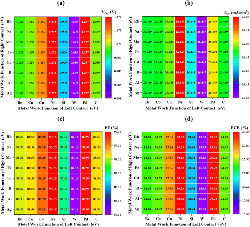
Fig. 2(a–d) presents the PV specifications of VOC, JSC, FF, and PCE for optimum double absorber structure (Devices-III), each utilizing different left and right contacts. It was found that employing Ni (nickel) and Ag (silver) as the left and right contacts yielded the best performance across all the metals. Nickel (Ni) is commonly selected as a metal contact in solar cells due to several key advantages over other metals. First, Ni has a relatively high work function (∼5.0 eV), which makes it particularly suitable for forming ohmic contacts with p-type semiconductors. This helps reduce contact resistance, facilitating more efficient charge extraction, which is crucial for enhancing the overall performance of the solar cell. Another major benefit is its excellent chemical stability. Nickel is less prone to oxidation compared to other metals such as aluminum or copper. This increased resistance to corrosion ensures that the metal contacts maintain their performance over extended periods, contributing to the long-term reliability and durability of the solar cell. Nickel also offers strong adhesion to a wide range of semiconductor materials, including silicon and perovskites, which are commonly used in various types of solar cells. This strong bonding reduces the likelihood of delamination or mechanical failures, particularly in flexible or thin-film solar cells. In terms of thermal stability, Ni can withstand higher temperatures during the fabrication process or during operation in hot environments without significant degradation. This thermal robustness makes it a preferred choice in solar cells that might be exposed to varying environmental conditions. Overall, compared to alternatives like aluminum or copper, nickel provides superior work function alignment, chemical and thermal stability, strong adhesion, and low diffusion rates, making it an excellent choice for metal contacts in a variety of solar cell technologies. With Ni and Ag designated as the corresponding left and right connections, the maximal PCE values recorded were 30.32%, JSC value was 26.45 mA cm−2; FF value was 90.15%; and VOC value was 1.27 V, respectively. Table 3 provides a complete list of both front and rear contact features.
 |
| | Fig. 2 Effect of metal in left touch for best Device-III (a) VOC, (b) JSC, (c) FF, and (d) PCE. | |
Table 3 Back and front contact parameters employed in the model
| Parameters |
Left contact (back) |
Right contact (front) |
| Surface recombination velocity of electrons (cm s−1) |
105 |
107 |
| Surface recombination velocity of holes (cm s−1) |
107 |
105 |
| Majority carrier barrier height (eV) relative to EF |
0.370 |
0.0200 |
| Majority carrier barrier height (eV) relative to EV |
0.2473 |
0.0020 |
| Work function (eV) |
Ni (5.35) |
Ag (4.52) |
| Temperature (K) |
275–475 |
275–475 |
3.2 Band diagram
Fig. 3(a–c) presents the band topologies of three distinct HTL-free PSCs that incorporate various light-absorbing materials, namely Sr3PBr3, Sr3NCl3, and a bilayer configuration of Sr3PBr3/Sr3NCl3. These illustrations offer a comprehensive overview of the properties associated with each type of PSC. In this context, the symbols denote specific energy levels within the band structure: EV (eV) stands for the peak energy level of the valence band, Fp (eV) signifies the Fermi level for holes, Fn (eV) denotes the Fermi level for electrons, and EC (eV) stands for the lowest energy level of the conduction band, correspondingly.
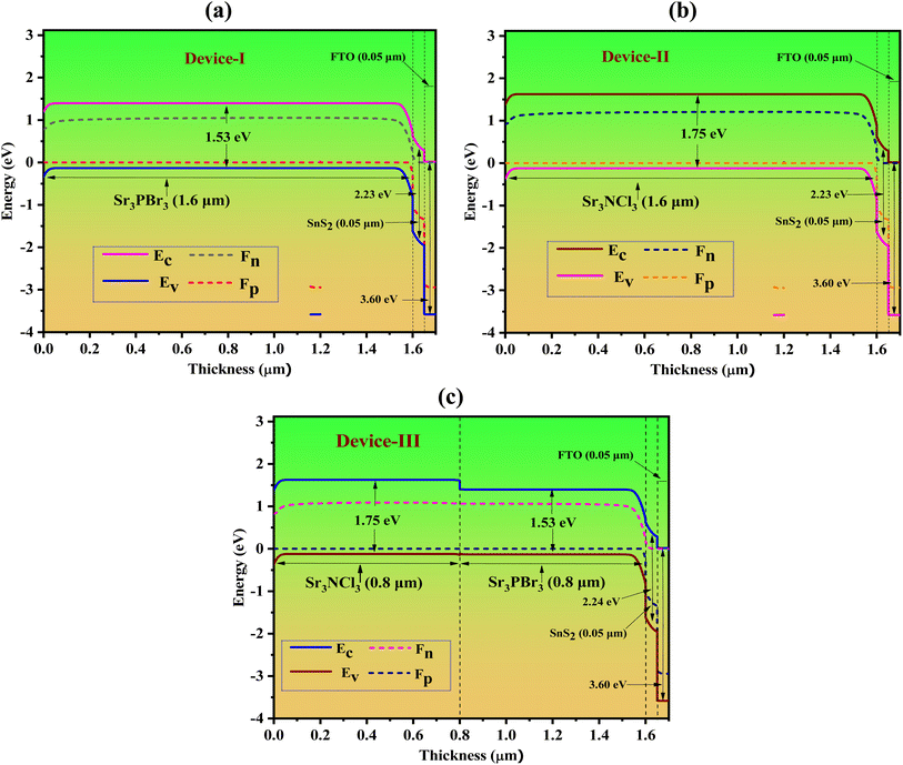 |
| | Fig. 3 A band configuration of three varieties of SCs, incorporating various substances that absorb light: (a) Sr3PBr3, (b) Sr3NCl3, (c) Sr3PBr3/Sr3NCl3 bilayer combination. | |
Conduction band offset (CBO) can be explained as follows: the energy difference observed between the lowest conduction band electron energy level in the perovskite layer and that in the ETL. In contrast, the valence band offset (VBO) indicates the energy difference involving the highest energy level of the valence band (VB) holes present in both the perovskite layer and the HTL. This study reveals that the bandgaps of the Sr3PBr3 and Sr3NCl3 perovskite materials are 1.53 eV and 1.75 eV, respectively. Furthermore, the energy gap of the FTO layer of the window is recorded at 3.6 eV, whereas the n-type SnS2 ETL shows an energy gap (Eg) of 2.23 eV.
3.3 Impact of the monolayer absorber's thickness, doping density, and defects
To find the best outcome for the two modeled single absorber-based systems, Fig. 4(a) shows the effect of changing the absorber width from 200 to 2000 nm. Absorber layer thickness is a key aspect in enhancing the effectiveness of thin-film PV cells.40 Given that the absorber's thickness in Device II increased during optimization, additionally, the opposite saturation current increased, resulting in a reduction of VOC, even with minor adjustments in thickness. However, for Device-I, changes in thickness had minimal impact on VOC. As the thickness increased, the spectral response extended to longer wavelengths, resulting in an increase in JSC, which eventually reached a saturation point across all proposed devices. In Devices-I and II, a thicker absorber led to a significant increase in FF. Efficiency for Devices I and II improved when the absorber thickness was appropriately set to around 1600 nm. With increased absorber thickness, more photons are absorbed, which also raises the recombination rate.41 Thus, the optimal absorber thickness was identified as 1600 nm to enhance performance for both Devices I and II. For Device-I, the optimal performance metrics included a PCE, FF, JSC, and VOC of 24.26%, 87.42%, 24.66 mA cm−2, and 1.13 V. For Device-II, the optimal values were a PCE, FF, JSC, and VOC of 20.35%, 87.91%, 18.07 mA cm−2, and 1.28 V. An optimal thickness of 1600 nm was determined for both devices of absorbers. To assess how the acceptor density affects (NA) within the layer of absorbers, it spans from 1013 to 1020 cm−3. Fig. 4(b) depicts the variations in FF, VOC, PCE, and JSC with different NA values. The JSC decreased from 27.35 to 24.98 mA cm−2 for Device-I and 20.19 to 17.57 mA cm−2 as NA increased while optimizing the process. As NA in the absorber layer rose, the Fermi level of holes decreased, leading to an increase in VOC for both devices. Additionally, the built-in potential increased with higher NA, which improved charge separation and contributed to the rise in VOC. However, both PCE and FF began to show improvement once NA surpassed 1017 cm−3. For NA variations ranging from 1013 to 1020 cm−3, Device-I achieved peak values of VOC at 1.13 V, JSC at 24.65 mA cm−2, FF at 87.42%, and PCE at 24.26%.
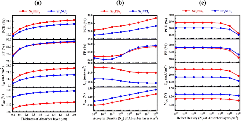 |
| | Fig. 4 An analysis of the role of (a) thickness, (b) doping concentration, and (c) defect density of the absorber layer in determining the performance of SCs in Devices I and II. | |
In contrast, Device-II reached PCE, FF, JSC, and VOC of 20.35%, 87.91%, 18.07 mA cm−2, and 1.28 V. It is possible to correlate the observed performance disparities to the increased defect states in the absorber layer, which arise from the higher NA values, as highlighted in the research. A 1017 cm−3 of NA was ideal determined for both devices of absorbers.
Recombination processes in photovoltaic systems can be influenced by defect density (Nt) fluctuations within the absorber layer, which can hinder the movement of carriers of charge and jeopardize the gadget's stability. An uneven distribution of defects across the absorber layer can modify its optical characteristics, impacting photon absorption and resulting in inconsistent performance across the device. To enhance photovoltaic effectiveness and dependability, reducing defect density and preserving homogeneity in the absorber layer are critical. Fig. 4(c) depicts the influence of different Nt levels on photovoltaic characteristics with a 1600 nm thick absorber. The analysis included the consequences of Nt values ranging from 1010 to 1017 cm−3 for Devices I and II. In these devices, the PCE, VOC, FF, and JSC exhibited significant declines as Nt grew from 1010 cm−3, with PCE dropping from 24.26% to 16.14% and from 20.35% to 15.15%, FF decreasing from 87.42% to 79.45% and from 87.91% to 82.04%, JSC falling from 24.65 to 19.12 mA cm−2 and from 18.07 to 14.95 mA cm−2, and VOC reducing from 1.13 to 1.06 V and from 1.28 to 1.24 V, respectively. For subsequent calculations, an optimal Nt of 1012 cm−3 was determined for both devices of absorbers.
3.4 The effect of active layer thickness on a double absorber device's output characteristic
Fig. 5 demonstrates the overall impact of the combined Dual Perovskite Absorber Layer (PAL) thicknesses. The x-axis denotes the width of Sr3PBr3, while the y-axis represents the thickness of Sr3NCl3. Simulation models were employed to assess the compatibility of various PAL thickness combinations, ranging from 200 nm to 2000 nm, as depicted in Fig. 5(a–d). The PV performance of the PSCs was examined to evaluate the optoelectrical properties under AM 1.5G lighting. The findings indicate that the VOC highest points at thinner PAL configurations, obtaining a maximum of 1.30 V, but falls as PAL thickness increases because of increased recombination rates, yielding a minimum of 1.23 V in Fig. 5(a). For the JSC, an ideal thickness of about 1 μm for Sr3PBr3 yields the best performance, achieving up to 27.40 mA cm−2. Conversely, thinner layers of Sr3PBr3 and Sr3NCl3 result in lower JSC values of around 19.62 mA cm−2 in Fig. 5(b) because there was insufficient photon absorption in the PALs, which adversely affects efficiency. The contour map found in Fig. 5(c) reveals that the highest FF of 90.12% is attained with varying PAL thickness values in the dual absorber configuration. Finally, Fig. 5(d) illustrates the combined influence of PAL thickness on PCE, with an optimized efficiency of 30.32% observed at a thickness of 0.8 μm for both Sr3PBr3 and Sr3NCl3. This is associated with a JSC of 26.44 mA cm−2 under similar thickness conditions, as PCE is immediately related to JSC. The analysis of contour provides essential perceptions of the design and performance enhancement of PSC devices.
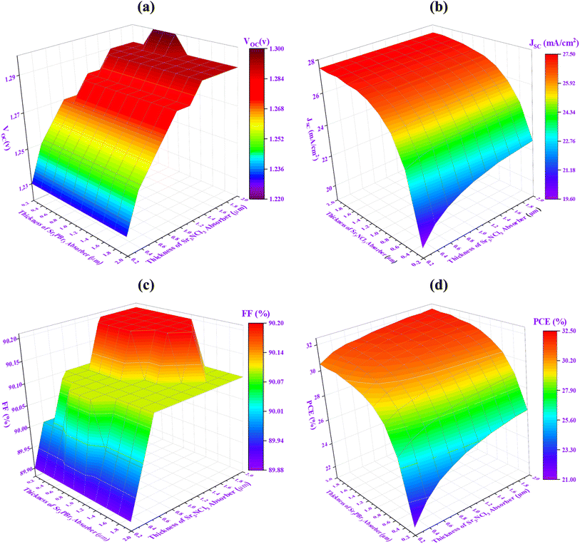 |
| | Fig. 5 The electrical specifications, which include (a) VOC, (b) JSC, (c) FF, and (d) PCE, were established by changing the two active layers' respective thicknesses. | |
3.5 Defect vs. doping of both absorber
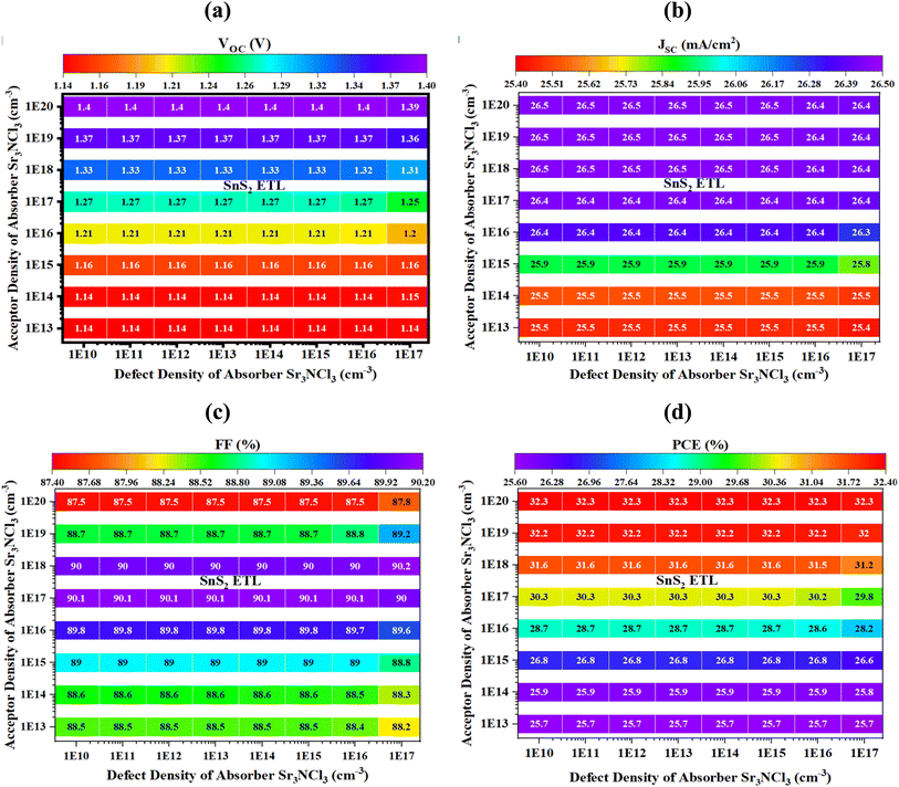
3.5.1 The relationship between doping concentration NA and defect density Nt in the Sr3PBr3 absorber layer. Selecting the right thickness of the absorber is essential when creating solar cells; however, the Nt and the NA also have a major impact on how well a gadget performs. An increase in Nt results in a higher number of defects, which raises carrier recombination rates and negatively impacts the gadget's total effectiveness.42,43 On the other hand, higher NA has been linked to better solar cell performance.44 Fig. 6 depicts the variation in key PV specifications PCE, VOC, FF, and JSC for Sr3PBr3-based PSCs depending on the x-axis absorber Nt and NA on the y-axis, spanning from 1010 to 1017 cm−3 and 1013 to 1020 cm−3. The functionality of the PSC remains consistent as soon as the Nt is lower than 1012 cm−3, irrespective of the levels of NA. However, when Nt exceeds 1012 cm−3, performance deteriorates due to defects acting as stages of trapping and recombination, which diminish effectiveness by restricting the availability of carriers of charge for electric current. These flaws also lead to shorter lifetimes of carriers, the material destabilizes and contributes to voltage drop. Therefore, minimizing defect density is vital for enhancing solar cell efficiency and reliability. Research indicates that achieving a defect density as low as Nt of 1012 cm−3 is the ideal value for improved performance.
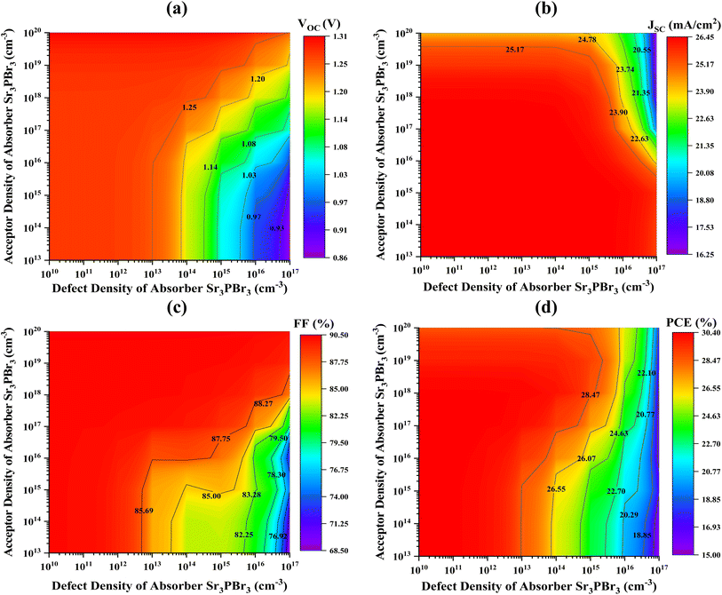 |
| | Fig. 6 Effects of the density of bulk defects adjustments vs. Sr3PBr3 absorber doping on PV characteristics; (a) VOC (b) JSC (c) FF and (d) PCE utilizing SnS2 as the ETL. | |
The absorber layer's NA is a key factor in figuring out the solar cell's PCE, as outlined in eqn (9). The PCE is intimately correlated with VOC, JSC, and FF, meaning that variations in NA can have a major effect on the device's overall performance.
| |
 | (9) |
where
Pin the measurement of incident power density is, represented in watts per square meter.
Fig. 6(d) illustrates that optimal peak PCE is attained when the NA is between 1013 to 1018 cm−3. This phenomenon arises from the contrasting behaviors of JSC and VOC about FF as the NA varies. As displayed in Fig. 6(a and b), both JSC and VOC maintain stability before the NA reaching 1018 cm−3; subsequently, a decline is observed except for FF. Conversely, FF, depicted in Fig. 6(c), shows an increase with greater doping concentrations. An increase in NA leads to a greater concentration of free carriers of charge, which improves charge separation effectiveness at the absorber/ETL contact, resulting in improved VOC and JSC due to a larger number of photogenerated carriers. However, as NA approaches the ND (donor doping concentration) of 1017 cm−3 of the ETL perovskite, the rate of recombination of charge increases, resulting in a reduction in both VOC and JSC. This heightened recombination, driven by the closeness of acceptor and donor dopants, negatively impacts the overall functionality of the apparatus. Conversely, FF experiences a positive effect from doping, because it displays how square the current–voltage qualities are. Enhanced doping improves the conductivity of the absorber layer, promoting effective transport of charge to the electrolytes, which reduces Rs (series resistance) and enhances FF. Doping also has an impact on shunt resistance, minimizing undesired current pathways and leaky currents, further aiding in the increase of FF. The relationship between FF and increased conductivity, alongside the rise in charge recombination, which adversely affects VOC and JSC, ultimately determines the effectiveness of PSCs. As the NA of the absorber nears the ND level of the ETL, a decline in PCE is observed. Achieving equilibrium between improved conductivity in addition to FF while minimizing recombination of charge is essential. The optimal concentration of NA at 1017 cm−3 and Nt of 1012 cm−3 results in a PCE of 30.32%, a VOC of 1.27 V, an FF of 90.14%, and a JSC of 26.44 mA cm−2.
3.5.2 Analyzing the effects of doping concentration NA and defect density Nt on the absorber layer of Sr3NCl3. Fig. 7 depicts the alteration in key PV parameters PCE, VOC, FF, and JSC for Sr3NCl3-based PSCs depending on the absorber Nt on the x-axis and NA on the y-axis, spanning from 1010 to 1017 cm−3 and 1013 to 1020 cm−3. An increase in Nt results in a higher number of defects, which raises carrier recombination rates and negatively impacts the gadget's total effectiveness. The performance of the PSC remains consistent at 1017 cm−3, irrespective of the levels of NA.
 |
| | Fig. 7 Effects of the density of bulk defects adjustments vs. Sr3NCl3 absorber doping on PV characteristics; (a) VOC (b) JSC (c) FF and (d) PCE utilizing SnS2 as the ETL. | |
Fig. 7(d) illustrates that the maximum PCE is attained when the doping concentration is between 1013 cm−3 and 1020 cm−3. This result is linked to the differing responses of the VOC and JSC in contrast to the FF as the doping concentration changes. As depicted in Fig. 7(a) and (b), both VOC and JSC maintain stability up to an NA value of 1020 cm−3, after which an increase is observed, except FF. Conversely, Fig. 7(c) shows that FF decreases with higher doping concentrations. An increase in NA results in a greater number of free carriers of charge, which enhances the effectiveness of charge separation at the interface between the absorber and ETL, thereby improving VOC and JSC because of the rise of photogenerated carriers. The overall PCE in PSCs is influenced by the interaction between FF and increased conductivity, along with increasing the charge recombination that adversely affects VOC and JSC. A decrease in PCE is observed as the NA level of the absorber approaches that of the ND level of the ETL. A need to strike a balance between improved conductivity and FF while minimizing charge recombination. The optimal parameters, with an Nt of 1012 cm−3 and an NA of 1017 cm−3 yield a PCE, VOC, JSC, and FF of 30.32%, 1.27 V, 26.44 mA cm−2, and 90.14%.
3.6 The impact of interface fault density Nt on the performance of bilayer perovskite solar cells
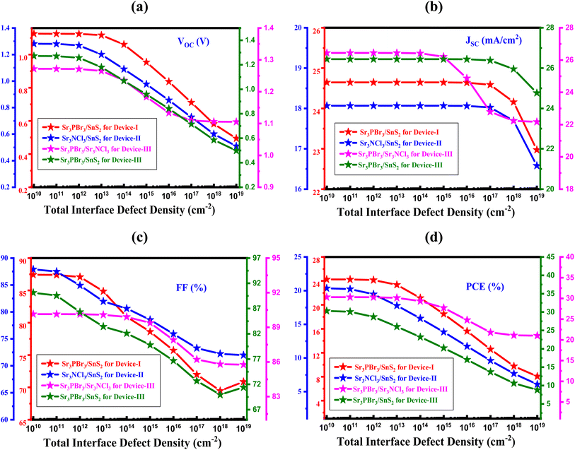
Interface defects (Ntf) arise from defects in the structure during the SC production procedure, which can severely affect the performance of solar panels at the contact by encouraging recombination of the charge carrier.45 Consequently, it is critical to assess their impact and optimize manufacturing specifications for practical applications. In this research, simulations were performed using a neutral Ntf of 1010 cm−2 across various interfaces: Sr3PBr3/SnS2 (Device I), Sr3NCl3/SnS2 (Device II), Sr3PBr3/Sr3NCl3 (Device III), and Sr3PBr3/SnS2 (Device III), while maintaining a defect level of 0.6 eV for all photovoltaic cells, as illustrated in Fig. 8(a–d). By adjusting Ntf from 1010 to 1019 cm−2, we assessed it's influence on photovoltaic parameters. The findings indicated that as Ntf increased, the PCE, FF, VOC, and JSC experienced significant declines: from 24.26% to 8.06%, 87.42% to 70.87%, 1.13 V to 0.49 V, and 24.65 to 22.97 mA cm−2 for Sr3PBr3/SnS2 (Device I); from 20.35% to 6.08%, 87.92% to 71.97%, 1.28 V to 0.51 V, and 18.07 to 16.58 mA cm−2 for Sr3NCl3/SnS2 (Device II); from 30.32% to 21.02%, 90.14% to 85.76%, 1.27 V to 1.11 V, and 26.44 to 22.17 mA cm−2 for Sr3PBr3/Sr3NCl3 (Device III); and from 30.32% to 8.82%, 80.14% to 71.41%, 1.27 V to 0.50 V, and 26.44 to 24.77 mA cm−2 for Sr3PBr3/SnS2 (Device III). The presence of Ntf generates recombination centers that hinder carrier transport efficiency, leading to reductions in FF and VOC. Moreover, series resistance might rise noticeably as a result of interface flaws, further compromising device performance.46 As the value of Ntf increases, the rate of carrier recombination at the interfaces also escalates, resulting in a reduction in overall execution.47,48 Thus, Ntf is recognized as a crucial factor affecting the performance characteristics of photovoltaic devices, especially at the interfaces of Sr3PBr3/SnS2 (Device I), Sr3NCl3/SnS2 (Device II), Sr3PBr3/Sr3NCl3 (Device III), and Sr3PBr3/SnS2 (Device III).49,50
 |
| | Fig. 8 Effects of interface densities of defect on the performance metrics of the PSC: (a) VOC, (b) JSC, (c) FF, and (d) PCE. | |
3.7 Enhancement of the thickness, concentration of carrier, and density of defect in the ETL layer
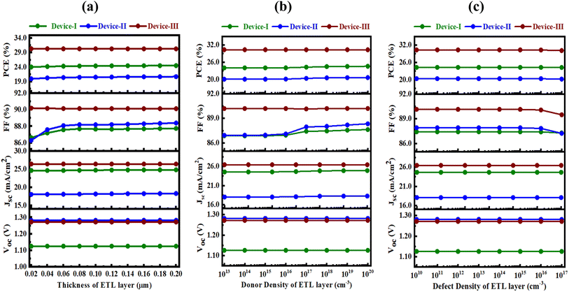
The PSC's effectiveness may be raised by adjusting the thickness of the ETL and reducing recombination currents.51 In this investigation, the thicknesses of SnS2 were adjusted between 20 and 200 nm, while keeping all other settings in Table 1 and 2 the same. Fig. 9(a) displays the influence of ETL thickness on photovoltaic metrics. An increase in ETL thickness resulted in negligible variations in VOC, JSC, and PCE, which exhibited slight enhancements in FF for all the devices. A thicker ETL layer tends to diminish light absorption and hinder charge generation and collection, leading to reduced transmittance and performance degradation, aligning with prior studies.52–54 For the SnS2 ETL, VOC, JSC, and PCE remain constant at 1.13 V, 1.28, and 1.27; 24.65, 18.23, and 26.44 mA cm2; 24.45%, 20.35%, and 30.32% for Devices-I, II, and III. The optimal ETL thicknesses were identified as 50 nm for SnS2. For Device III FF remains constant at 90.02%, but a small change in Devices I and II from 86.63% to 87.74% and 86.30% to 88.39%. Fig. 9(b) analyzes how varying donor doping concentrations (ND) influence the PV characteristics of ETL. Regarding the instance of the SnS2 ETL, the VOC, JSC, and PCE exhibited relative stability up to an ND of 1017 cm−3, remaining constant at 1.13 V, 1.28, and 1.27; 24.65, 18.00, and 26.44 mA cm2; 24.45%, 20.35%, and 30.32% for Device-I, II, and III. For device III, FF remains constant at 90.02%, but a small change in Devices I and II from 86.87% to 87.63% and 86.93% to 88.33%.
 |
| | Fig. 9 Influence of (a) thickness, (b) doping concentration, and (c) defect density of the ETL layer on Devices I, II, and III's solar cell performance. | |
The optimal doping concentration for SnS2 ETL was determined to be 1017 cm−3. The presence of the density of the defect results in the entrapment of photogenerated carriers, which triggers the Shockley–Read–Hall (SRH) rearranging of molecules. When the SnS2 buffer layer is thicker, photogenerated electrons are required to traverse a longer distance to make touch with the front, therefore raising the possibility of recombination of the carrier. A rise in carrier concentration reduces the average free route, which in turn elevates recombination rates. The solar cells' efficiency is notably compromised due to SRH recombination linked to heightened bulk defects. For all devices, the PV parameters remain unchanged except FF, which has few changes. To enhance cell performance in real-world manufacturing conditions, defect density must be maintained at or below 1014 cm−3 (in Fig. 9(c)). As a result, the optimal doping levels, thickness, and defect density have been established at 1017 cm−3, 0.05 μm, and 1014 cm−3, respectively, to encourage efficient use of materials and photon transfer in the ETL layer.
3.8 Significance of series and shunt resistances
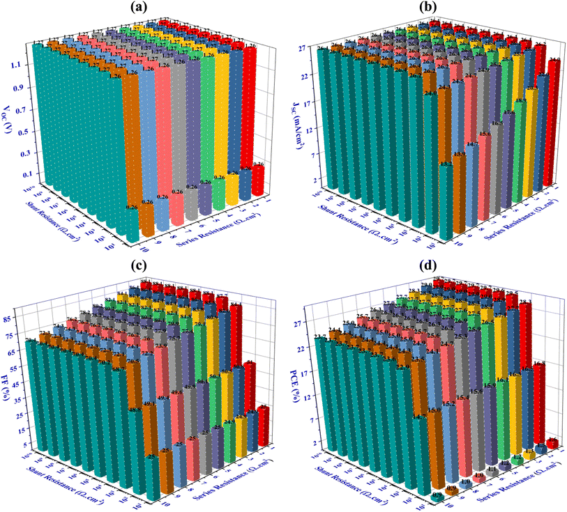
Fig. 10 demonstrates the impact of shunt resistance (Rsh) and series resistance (Rs) on solar panel execution. Series resistance describes the electrical resistance faced by the device when it is connected to external loads via its contacts, while shunt resistance pertains to the leaking currents happening at the boundaries of the panel. In this analysis, Rsh and Rs were adjusted inside the ranges of 1 to 10 Ω cm2 and 10 to 1010 Ω cm2, respectively. The results indicate that both Rs and Rsh have a significant effect on PCE, as illustrated in Fig. 10(d). For optimal performance, it is advantageous to have as much as possible lower Rs and a higher Rsh.55 Specifically, Fig. 10(d) displays that the PCE is more affected by shunt resistance, while the FF is more responsive to series resistance, as depicted in Fig. 10(c). Additionally, Fig. 10(a–b) reveals that changes in series resistance notably influence the VOC and JSC. The data indicates that as Rsh and Rs vary from 10 to 1010 Ωcm2 and 1 to 10 Ω cm2, correspondingly, the JSC, PCE, VOC, and FF range from 26.44 to 13.22 mA cm−2, 29.65% to 0.87%, 1.27 to 0.26 V, and 88.11% to 25.01%. This suggests that maximizing shunt resistance to minimize leakage currents and minimizing series resistance to improve carrier collection efficiency leads to the highest PCE.
 |
| | Fig. 10 The contribution of shunt and series resistance to the overall electrical execution of PSCs is demonstrated in terms of (a) VOC, (b) JSC, (c) FF, and (d) PCE, specifically for the optimized structure of (FTO/SnS2/Sr3PBr3/Sr3NCl3/Ni). | |
3.9 The significance of operating temperature on a solar cell's efficiency
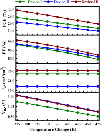
The analysis presented in Fig. 11 demonstrates how temperature affects the execution metrics of Devices I, II, and III within a temperature spectrum of 275–475 K. The findings disclose that while the JSC remains largely unchanged with rising temperatures, the FF, VOC, and PCE experience a downward trend. This finding suggests that higher temperatures might enhance the charge carriers' thermal mobility in SCs, which could help sustain or marginally increase JSC. Conversely, higher temperatures may lead to how the absorber layer acts more like a conductor that is ohmic, which can impede the transport of the carrier and result in heat produced by electrical energy conversion, thereby diminishing FF, PCE, and VOC.56,57 Additionally, inadequate thermal dissipation in the various elements that make up the PSC can further raise temperatures, offering a chance for gadget harm. As a result, it is imperative to thoroughly evaluate the thermal tolerance of every absorber layer throughout the design of interconnected SCs. The results indicate that the JSC values for Devices I, II, and III remain consistent at 24.64, 18.07, and 26.44 mA cm−2, respectively, while the VOC experiences a decline from 1.17 to 0.81 V for Device I, from 1.33 to 0.92 V for Device II, and from 1.32 to 0.91 V for Device III as temperature increases. In a similar vein, the FF decreases from 88.30% to 79.55% for Device I, from 88.59% to 81.12% for Device II, and from 90.93% to 82.13% for Device III. As a result, the efficiency peaks at lower temperatures, reaching 25.42%, 21.27%, and 31.74% for Devices I, II, and III, respectively, but subsequently drops to 15.83%, 13.54%, and 19.72% as temperatures rise, as illustrated in Fig. 11.
 |
| | Fig. 11 The effect of temperature changes on solar cells. | |
3.10 The absorption coefficient for every layer in the system
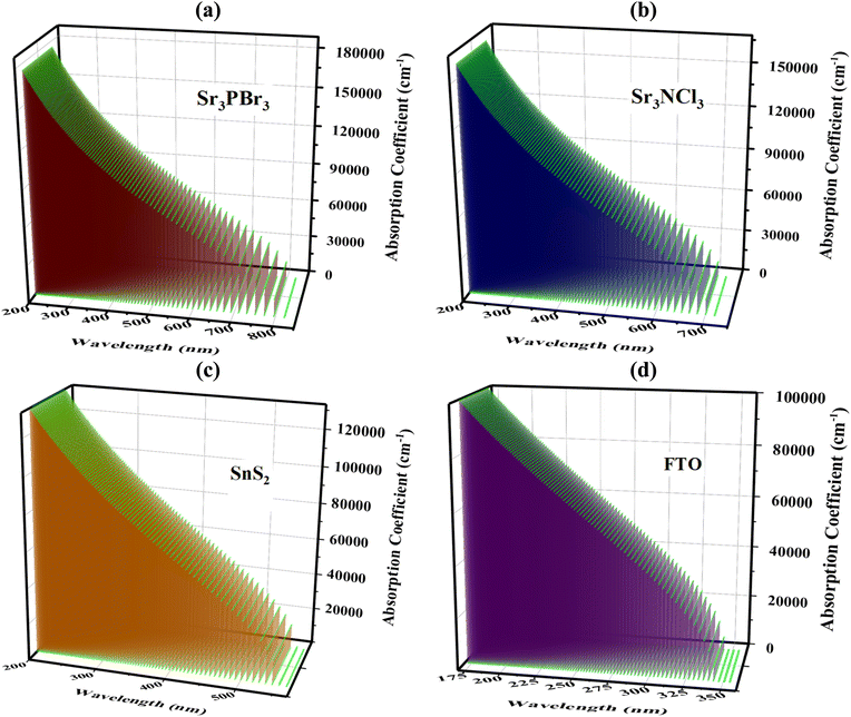
An important metric for determining a material's ability to absorb light energy is the optical absorption coefficient, having a major impact on determining the PCE of solar cells.58,59 For solar panels, the first absorption peak is very crucial, as it reveals the specific wavelengths of luminosity that the material can effectively capture.60–62 The materials Sr3PBr3, Sr3NCl3, SnS2, and FTO are linked to the FTO/SnS2/absorber (Sr3PBr3/Sr3NCl3) solar cell configuration. Fig. 12 depicts the changes in absorption coefficients across various wavelengths for these materials. Notably, Sr3PBr3 and Sr3NCl3 exhibit pronounced absorption peaks at a wavelength of 200 nm, while the FTO material peaks at 172.22 nm.
 |
| | Fig. 12 An analysis of the absorption coefficient is conducted for the ideal SC architecture of FTO/SnS2/Sr3PBr3/Sr3NCl3/Ni, specifically for the materials: (a) Sr3PBr3, (b) Sr3NCl3, (c) SnS2, and (d) FTO. | |
In contrast, SnS2 shows a significant absorption peak at 200 nm. The optical absorption spectra for each material reveal the peak absorption points within the ultraviolet and visible light ranges. As illustrated in Fig. 12(a–d), the maxima of absorption for Sr3PBr3, Sr3NCl3, SnS2, and FTO are measured at 174![[thin space (1/6-em)]](https://www.rsc.org/images/entities/char_2009.gif) 857.55 cm−1, 159
857.55 cm−1, 159![[thin space (1/6-em)]](https://www.rsc.org/images/entities/char_2009.gif) 461.33 cm−1, 132
461.33 cm−1, 132![[thin space (1/6-em)]](https://www.rsc.org/images/entities/char_2009.gif) 958.86 cm−1, and 100
958.86 cm−1, and 100![[thin space (1/6-em)]](https://www.rsc.org/images/entities/char_2009.gif) 000 cm−1, respectively. To ensure that materials with bandgaps of 1.53 eV and 1.75 eV achieve adequate absorbance of light in the visible spectrum for optimal solar cell execution, targeted strategies should be implemented.
000 cm−1, respectively. To ensure that materials with bandgaps of 1.53 eV and 1.75 eV achieve adequate absorbance of light in the visible spectrum for optimal solar cell execution, targeted strategies should be implemented.
3.11 The attributes of J–V and Q-E
PSCs' affordability and great efficiency have sparked a lot of interest in them, positioning them as a promising category of photovoltaic technology. Evaluating their performance requires a thorough examination of two essential parameters: current density–voltage (J–V) characteristics and quantum efficiency (Q-E).63,64 The current density measured at zero voltage indicates the peak current the cell can generate when exposed to light, while the voltage measured at no current signifies the highest voltage that the cell is capable of. QE quantifies the proportion of carriers of charge successfully gathered by the cell about the number of photons that arrive, serving as a metric for the cell's capability to convert incoming photons into electrical energy that may be used.21,65 Q-E is wavelength-dependent, demonstrating the solar spectrum's efficiency of the cell and identifying the wavelengths at which it operates most effectively. This evaluation also uncovers losses due to reflectance, transmission, and recombination without radiation, offering critical insights that can inform enhancements in cell design.
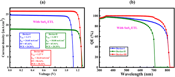
Fig. 13(a and b) display the J–V and Q-E features for the configurations of Devices I, II, and III. The optimized designs yielded PCE values of 24.26%, 20.35%, and 30.32% for Devices I, II, and III, respectively. These devices also exhibited FF values of 87.42%, 87.90%, and 90.14%, JSC values of 24.65, 18.07, and 26.44 mA cm−2, and VOC values of 1.13, 1.28, and 1.27 V. It is noteworthy that the current density in these optimized structures reaches zero at voltages of 1.14 V, 1.3 V, and 1.28 V for Devices I, II, and III, respectively. Prior studies have consistently demonstrated that current density decreases with increasing voltage,66,67 as shown in Fig. 13(a). The Q-E profiles presented in Fig. 13(b) cover a wavelength that varies from 300 to 1200 nm, beginning at nearly 100% and then progressively dropping to 0% as the wavelengths approach 710 nm for Device II and 810 nm for Devices I and III. For most photovoltaic systems, quantum efficiency (QE) values close to 100% throughout a wide wavelength range, such 350–700 nm, are regarded as impractical because of several basic and real-world constraints:
 |
| | Fig. 13 An examination of the (a) J–V and (b) Q-E curves associated with both frameworks is provided. | |
(1) Losses of materials and devices: several losses often encountered by photovoltaic materials and devices keep QE from reaching 100%. These losses consist of partial photon absorption, recombination, and reflection. Since each material has intrinsic absorption and efficiency restrictions based on its bandgap and electrical structure, even highly tailored substances are unlikely to absorb and convert almost every photon across such a large range. Recombination mechanisms: in practical devices, QE is decreased by carrier recombination, particularly Shockley–Read–Hall, Auger, and surface recombination. Since recombination losses rely on the intrinsic qualities of the material and the caliber of the interfaces inside the device, they are almost hard to completely remove.
(2) Thermal effects: QE is further constrained by thermal losses and optical losses, such as light absorption and scattering outside the active layer. For example, photons at energies much beyond the bandgap may lose energy as heat, even in well-designed systems, which lowers the external QE at those wavelengths.
(3) Comparing with empirical data: in reality, even extremely efficient solar cells, like those made of perovskite or gallium arsenide (GaAs), exhibit QE peaks at particular wavelengths but not throughout the visible spectrum. GaAs solar cells, for instance, can reach a high QE of about 90% in the region of peak absorption, but they usually do not sustain such values throughout the visible spectrum.
In conclusion, structural recombination is crucial in determining solar cell efficiency, particularly in devices with many interfaces or in thin-film and polycrystalline cells where layer interfaces and grain boundaries are frequent. Here are some references of QE that reach almost 100% at 350 to 750 nm:
• This book covers the fundamentals of solar cell physics and explains why intrinsic losses like recombination and reflection make it challenging to get QE around 100% at wide wavelengths.68
• This groundbreaking study outlines the theoretical effectiveness limitations of solar cells, demonstrating that the maximum QE is limited to less than 100% throughout a large spectral range by variables such as heat losses and recombination.69
• Recent studies that showed QE reaches almost 100% at 350–750 nm.27,70
The decline in Q-E aligns with the patterns noted in the J–V profiles. A summary of the optimized simulation results for the final solar cells is available in Table 4, which allows for further comparison with earlier studies.
Table 4 The metrics for PV performance acquired in this investigation are juxtaposed with those found in the literature regarding other double absorber configurations (note: E denotes experimental work and T represents theoretical work)
| Structure |
Type of work |
VOC (V) |
JSC (mA cm−2) |
FF (%) |
PCE (%) |
Ref. |
| Device-I |
T |
1.13 |
26.65 |
87.08 |
24.26 |
This work |
| Device-II |
T |
1.28 |
18.07 |
87.91 |
20.35 |
This work |
| Device-III |
T |
1.27 |
26.44 |
90.14 |
30.32 |
This work |
| CsPbI3/CsSnI3 |
T |
0.96 |
26.59 |
78.41 |
19.99 |
71 |
| MASnI3/MAPBr3 |
T |
1.04 |
31.77 |
78.78 |
25.91 |
72 |
| CsPbI3/Cs0.25FA0.75PbI3 |
E |
1.20 |
18.91 |
76.00 |
17.39 |
73 |
| CsPbI3/FAPbI3 |
T |
1.10 |
24.50 |
74.00 |
19.94 |
74 |
| CsPbI3/CsGeI3 |
T |
1.19 |
23.45 |
86.19 |
24.06 |
75 |
| CsPbI3/FAPbI3 |
E |
1.22 |
17.26 |
74.00 |
15.60 |
76 |
| CsSnGeI3/CsSnI3 |
T |
– |
– |
– |
28.61 |
77 |
| MAPbBr3/CsPbBr3 |
T |
– |
– |
– |
6.53 |
78 |
| Cs3Bi2I9/La2NiMnO6 |
T |
0.87 |
42.70 |
75.01 |
26.02 |
79 |
3.12 Shape of the G-R profile and the importance of absorber layer thickness
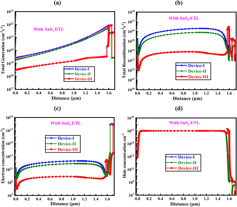
Fig. 14(a and b) display the rates of recombination and carrier production for both frameworks at various places. In the course of carrier generation, electron–hole pairs are created when an electron travels from the VB to the CB, leaving the hole in the VB. This transition is observed in Sr3PBr3 and Sr3PNCl3, which facilitates the discharge of holes and electrons, thereby generating additional carriers.80–82 For all the devices, the carrier generation rate is lowest near 1 mm and reaches its maximum around 1.6 μm. These differences can be explained by the fact that various places have variable rates of photon absorption. The generation of carrier rate, G(x), is calculated using eqn (10), On the other hand, the Nphot (λ, x) of the SCAPS-1D model evaluates the production of electron–hole pairs according to the incident photon flux.60| | |
G(λ, x) = α(λ, x)Nphot(λ, x)
| (10) |
 |
| | Fig. 14 Influence of absorber layer thickness on (a and b) carrier generation and recombination rates (c and d) electron and hole concentration. | |
In solar systems, the recombination of holes and electrons takes place within the conduction band. The rates of recombination in well-optimized PSCs are significantly affected by the effectiveness and durability of these carriers of charge, along with the presence of defect states in each layer. Increased recombination rates are observed when electrons overcome the energy barrier and combine with gaps present in the conduction band's valence band. The energy levels connected to this transition are also essential in figuring out how quickly electron–hole pairs recombine. Fig. 14(c and d) depict how differences in the absorber layer and ETL thickness affect the hole and electron carrier concentrations. Changes in absorber thickness influence hole concentration due to varying densities of states (DOS) within the VBs. Notably, greater concentrations of carriers, particularly in the comparison of electron and hole densities, are more evident. The research indicates that employing SnS2 as the ETL alongside the (Sr3PBr3/Sr3NCl3) absorber minimizes hole–electron recombination and increases carrier production, which improves the absorber material's efficiency. These insights could pave the way for the advancement of highly efficient PSCs.
4. Framework for conducting experimental validation
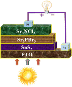
Recent investigations into Sr3PBr3 and Sr3NCl3-based solar cells faced challenges regarding performance when utilizing SnS2 as the ETL. Nevertheless, substantial advancements were achieved earlier this year, culminating in an impressive efficiency of 20.77% and 18.11%, which reflects a steady annual enhancement in the photovoltaic performance of Sr3PBr3 and Sr3NCl3. This research pinpointed an optimal configuration, as depicted in Fig. 15, that reached an outstanding peak efficiency of 30.32%. This achievement was realized by employing SnS2 as the ETL, JSC, FF, and VOC values of 26.44 mA cm−2, 90.14%, and 1.27 V, respectively. To enhance the accuracy of simulation results, Sr3PBr3/Sr3NCl3 a thorough methodology that includes material synthesis, device manufacturing, characterization, performance assessment, and stability testing-all of which are included in Table 4 should be used to experimentally evaluate solar cell technologies.
 |
| | Fig. 15 The improved optimized framework construction. | |
Several factors contribute to the higher performance of the devices compared to the reference values in Table 4. First, the selected absorber materials, Sr3PBr3 and Sr3NCl3, may possess superior optical and electrical properties, enhancing charge separation and transport. Effective band alignment between the layers reduces energy losses during charge extraction, leading to improved VOC and JSC. Additionally, optimized interfaces can minimize recombination losses, further boosting efficiency. To ensure an accurate comparison between theoretical work and experimental results, controlled experimental conditions were maintained to standardize the testing environment. Theoretical predictions were validated against established models and known experimental data. Consistent measurement techniques for key metrics, along with statistical analysis of multiple samples, ensured reliable results. Lastly, all methods and findings were transparently reported to enable reproducibility and verification by others in the field.
5. Conclusions
This research focused on utilizing SCAPS-1D applications to simulate a heterojunction without lead, PSC composed of Sr3PBr3/Sr3NCl3. The simulation process commenced with the establishment of the absorber layer by employing perovskite components, while SnS2 was integrated as the ETL. The effects of different absorber layer thicknesses were assessed in the study, as were doping concentrations and defect densities, in addition to the doping and thickness of the ETL, on the overall execution. Furthermore, the simulations investigated how temperature, series, and shunt resistance influenced the electrical characteristics under standard test conditions (STC). The results showed that the new prototype's maximum simulated efficiency achieved 30.32%, with a VOC of 1.27 V, an FF of 90.14%, and a JSC of 26.44 mA cm−2, achieved with approximately 800 nm thickness for both Sr3PBr3 and Sr3NCl3. Optimal doping concentrations were identified at around 1017 cm−3 for each perovskite, while a recommended defect density was approximately 1012 cm−3. To ensure stable performance, attention must be given to the absorber layer, FTO, and ETL during the manufacturing process. The study recommends maintaining the PSC's operating temperature near 300 K for best results. Future investigations should encompass experimenting with validation of stability and longevity in real-world scenarios, as well as a deeper exploration of the prototype's performance of several HTL, FTO, and ETL materials. This double absorber solar cell innovatively uses two light-absorbing materials, each optimized to capture different parts of the solar spectrum. This design enhances efficiency by reducing energy loss and utilizing a broader range of sunlight. The first absorber captures high-energy photons, while the second harnesses lower-energy photons. This tandem structure boosts overall solar energy conversion efficiency compared to traditional single-absorber cells.
List of abbreviations
| QE | Quantum efficiency |
| Op | Optimized |
| VOC | Open circuit current |
| WF | Work function |
| Rs, Rsh | Series (shunt) resistance |
| χ | Electron affinity |
| PV | Photovoltaic |
| J–V | Current density – voltage |
| ND | Shallow donor density |
| μn, μh | Electron (hole) mobility |
| FTO | Fluorine-doped tin oxide |
| EBD | Energy band diagram |
| VBO | Valence band offset |
| NA | Shallow acceptor density |
| CBO | Conduction band offset |
| VB | Valence band |
| PSC | Perovskite solar cell |
| ETL, HTL | Electron (hole) transport layer |
| SRH | Shockley–Read–Hall |
| SCAPS | Solar cell capacitance simulator |
| NV | Effective density valence band |
| JSC | Short circuit current density |
| NC | Effective density of conduction band |
| FF | Fill factor |
| PCE | Power conversion efficiency |
| ∈r | Dielectric permittivity (relative) |
| BMS | Back metal contact |
| Nt | Defect density |
Ethical approval
All the authors declare that the manuscript does not have studies on human subjects, human data or tissue, or animals.
Data availability
Data will be made available on reasonable request.
Author contributions
Md. Shamim Reza, and Avijit Ghosh: conceptualization, methodology, software, validation, formal analysis, visualization, investigation, data curation, supervision, writing – original draft, and review and editing. Nidhal Drissi, Hmoud Al-Dmour, and Md. Selim Reza: software, validation, formal analysis, data curation, writing – original draft, and review and editing. Ripan Kumar Prodhan, Majharul Islam, Sabina Sultana, and Shirin Begum: software, validation, formal analysis, writing – original draft, and review and editing.
Conflicts of interest
The authors have no conflicts of interest.
Acknowledgements
The authors extend their appreciation to the Deanship of Research and Graduate Studies at King Khalid University for funding this work through Large Research Project under grant number RGP.2/197/45.
References
- M. Z. Jacobson and M. A. Delucchi, Providing all global energy with wind, water, and solar power, Part I: Technologies, energy resources, quantities and areas of infrastructure, and materials, Energy Pol., 2011, 39(3), 1154–1169 CrossRef CAS.
- A. GhaffarianHoseini, N. D. Dahlan, U. Berardi, A. GhaffarianHoseini, N. Makaremi and M. GhaffarianHoseini, Sustainable energy performances of green buildings: A review of current theories, implementations and challenges, Renew. Sustain. Energy Rev., 2013, 25, 1–17 CrossRef.
- T. S. Ge, R. Z. Wang, Z. Y. Xu, Q. W. Pan, S. Du and X. M. Chen, et al., Solar heating and cooling: Present and future development, Renew. Energy, 2018, 126, 1126–1140 CrossRef.
- A. DiCarlo, E. Lamanna and N. Y. Nia, Photovoltaics, EPJ Web Conf., 2020, vol. 246 Search PubMed.
- K. Takanabe, Photocatalytic Water Splitting: Quantitative Approaches toward Photocatalyst by Design, ACS Catal., 2017, 7(11), 8006–8022 CrossRef CAS.
- T. Jafari, E. Moharreri, A. Amin, R. Miao, W. Song and S. Suib, Photocatalytic Water Splitting—The Untamed Dream: A Review of Recent Advances, Molecules, 2016, 21(7), 900 CrossRef.
- V. Kanneboina, Detailed review on c-Si/a-Si:H heterojunction solar cells in perspective of experimental and simulation, Microelectron. Eng., 2022, 265, 111884 CrossRef CAS.
- B. Salhi, The Photovoltaic Cell Based on CIGS: Principles and Technologies, Materials, 2022, 15(5), 1908 CrossRef CAS.
- Y. Wang, G. Wang, Y. Zhou, Q. Xie, J. Chen and K. Zheng, et al., Research progress in doped absorber layer of CdTe solar cells, Renew. Sustain. Energy Rev., 2023, 183, 113427 CrossRef CAS.
- Q. Zhao, R. Han, A. R. Marshall, S. Wang, B. M. Wieliczka and J. Ni, et al., Colloidal Quantum Dot Solar Cells: Progressive Deposition Techniques and Future Prospects on Large-Area Fabrication, Adv. Mater., 2022, 34(17), 2107888 CrossRef CAS.
- Y. Liu, B. Liu, C.-Q. Ma, F. Huang, G. Feng and H. Chen, et al., Recent progress in organic solar cells (Part I material science), Sci. China Chem., 2022, 65(2), 224–268 CrossRef CAS.
- X. Luo, X. Lin, F. Gao, Y. Zhao, X. Li and L. Zhan, et al., Recent progress in perovskite solar cells: from device to commercialization, Sci. China Chem., 2022, 65(12), 2369–2416 CrossRef CAS.
- M. A. Green, E. D. Dunlop, M. Yoshita, N. Kopidakis, K. Bothe and G. Siefer, et al., Solar cell efficiency tables (version 62), Prog. Photovoltaics Res. Appl., 2023, 31(7), 651–663 CrossRef.
- D. Zhang, H. Zhang, H. Guo, F. Ye, S. Liu and Y. Wu, Stable α-FAPbI 3 in Inverted Perovskite Solar Cells with Efficiency Exceeding 22% via a Self-Passivation Strategy, Adv. Funct. Mater., 2022, 32(27), 2200174 CrossRef CAS.
- X. Zhou, L. Zhang, H. Hu, Z. Jiang, D. Wang and J. Chen, et al., Highly efficient and stable hole-transport-layer-free inverted perovskite solar cells achieved 22% efficiency through p-type molecular synergistic doping, Nano Energy, 2022, 104, 107988 CrossRef CAS.
- J. L. Prasanna, E. Goel, A. Kumar and A. Kumar, Reduced interfacial recombination in perovskite solar cells by structural engineering simulation, J. Opt., 2022, 24(11), 115901 CrossRef CAS.
- S. Bhattarai, M. K. Hossain, G. F. I. Toki, R. Pandey, J. Madan and D. P. Samajdar, et al., Efficiency enhancement of perovskite solar cell devices utilizing MXene and TiO 2 as an electron transport layer, New J. Chem., 2023, 47(38), 17908–17922 RSC.
- J. L. Prasanna, E. Goel, A. Kumar and A. Kumar, Computational Study of Double Absorber layer Perovskite Solar Cell Devices, In: 2022 IEEE 19th India Council International Conference (INDICON). IEEE, 2022, pp. 1–6 Search PubMed.
- S. Bhattarai, M. K. Hossain, R. Pandey, J. Madan, D. P. Samajdar and M. F. Rahman, et al., Perovskite Solar Cells with Dual Light Absorber Layers for Performance Efficiency Exceeding 30%, Energy Fuels, 2023, 37(14), 10631–10641, DOI:10.1021/acs.energyfuels.3c01659.
- A. Ghosh, M. Ferdous Rahman, A. Kuddus, M. K. A. Mohammed, M. Rasidul Islam and S. Bhattarai, et al., Investigating of novel inorganic cubic perovskites of A3BX3 (A=Ca, Sr, B P, As, X=I, Br) and their photovoltaic performance with efficiency over 28, J. Alloys Compd., 2024, 986, 174097 CrossRef CAS . available from: https://linkinghub.elsevier.com/retrieve/pii/S0925838824006844.
- M. A. Rahman, M. F. Rahman, L. Marasamy, M. Harun-Or-Rashid, A. Ghosh and A. R. Chaudhry, et al., Impact of A-Cations Modified on the Structural, Electronic, Optical, Mechanical, and Solar Cell Performance of Inorganic Novel A 3 NCl 3 (A = Ba, Sr, and Ca) Perovskites, Energy Fuels, 2024 DOI:10.1021/acs.energyfuels.4c00525.
- J. Li, J. Xiao, T. Lin, Z. Yan and X. Han, Lanthanide doping enabled multimodal luminescence in layered lead-free double perovskite Cs 4 MnBi 2 Cl 12, J. Mater. Chem. C, 2022, 10(19), 7626–7632 RSC.
- C. Su, Z. Zhang, J. Yao, M. Chen, P. Huang and Y. Zhang, et al., Construction, photoelectric response and phase transition for new hybrid double perovskites showing narrow band gaps, Chin. Chem. Lett., 2023, 34(4), 107442 CrossRef CAS.
- R. Hooijer, A. Weis, A. Biewald, M. T. Sirtl, J. Malburg and R. Holfeuer, et al., Silver-Bismuth Based 2D Double Perovskites (4FPEA) 4 AgBiX 8 ( X = Cl, Br, I): Highly Oriented Thin Films with Large Domain Sizes and Ultrafast Charge-Carrier Localization, Adv. Opt. Mater., 2022, 10(14), 2200354 CrossRef CAS.
- A. J. Kale and A. Dixit, Vacancy ordered Cs2SnX6 (X = Cl, Br, I) double perovskites as an absorber and antiferromagnetic NiO with GO as a hole transport layer for highly efficient heterojunction solar cell application, Sol. Energy, 2022, 247, 330–345 CrossRef CAS.
- H. Saci, B. Bouabdallah, N. Benseddik, Z. Nabi, B. Bouhafs and B. Benichou, et al., Optoelectronic properties and lattice thermal conductivity of Cs2CuBiX6 (X = F, Cl, Br, I) double perovskites: Thermodynamic and ab initio approaches, Comput. Condens. Matter, 2023, 35, e00791 CrossRef.
- R. M. Shamim, A. Ghosh, A. Kalam Azad, M. Selim Reza, M. Mahfuz Hossain and A. Ahammad Miazee, et al., Boosting the effectiveness of a cutting-edge Ca3NCl3 perovskite solar cell by fine-tuning the hole transport layer, Mater. Sci. Eng. B, 2024, 309, 117656 CrossRef . available from: https://linkinghub.elsevier.com/retrieve/pii/S0921510724004859.
- M. Batzill and U. Diebold, The surface and materials science of tin oxide, Prog. Surf. Sci., 2005, 79(2–4), 47–154 CrossRef CAS.
- D. S. Ginley and C. Bright, Transparent Conducting Oxides, MRS Bull., 2000, 25(8), 15–18 CrossRef CAS.
- C. G. Granqvist, Transparent conductors as solar energy materials: A panoramic review, Sol. Energy Mater. Sol. Cells, 2007, 91(17), 1529–1598 CrossRef CAS.
- M. S. Reza, M. F. Rahman, A. Kuddus, M. K. A. Mohammed, A. K. Al-Mousoi and M. R. Islam, et al., Boosting efficiency above 28% using effective charge transport layer with Sr 3 SbI 3 based novel inorganic perovskite, RSC Adv., 2023, 13(45), 31330–31345 RSC . available from: http://xlink.rsc.org/?DOI=D3RA06137J.
- M. Burgelman, K. Decock, S. Khelifi and A. Abass, Advanced electrical simulation of thin film solar cells, Thin Solid Films, 2013, 535(1), 296–301 CrossRef CAS.
- M. A. Ashraf and I. Alam, Numerical simulation of CIGS, CISSe and CZTS-based solar cells with In 2 S 3 as buffer layer and Au as back contact using SCAPS 1D, Eng. Res. Express, 2020, 2(3), 035015 CrossRef.
- L. ∼I. Nykyruy, R. ∼S. Yavorskyi, Z. ∼R. Zapukhlyak, G. Wisz and P. Potera, Evaluation of CdS/CdTe thin film solar cells: SCAPS thickness simulation and analysis of optical properties, Opt. Mater., 2019, 92, 319–329 CrossRef CAS.
- N. K. Bansal, S. Mishra, H. Dixit, S. Porwal, P. Singh and T. Singh, Machine Learning in Perovskite Solar Cells: Recent Developments and Future Perspectives, Energy Technol., 2023, 11(12), 2300735 CrossRef.
- K. T. Arockiya-Dass, K. Sekar and L. Marasamy, Theoretical Insights of Degenerate ZrS 2 as a New Buffer for Highly Efficient Emerging Thin-Film Solar Cells, Energy Technol., 2023, 11(9), 2300333 CrossRef CAS.
- M. Burgelman, P. Nollet and S. Degrave, Modelling polycrystalline semiconductor solar cells, Thin Solid Films, 2000, 361–362, 527–532 CrossRef CAS . available from: https://linkinghub.elsevier.com/retrieve/pii/S0040609099008251.
- G. Kumar, B. K. Ravidas, S. Bhattarai, M. K. Roy and D. P. Samajdar, Exploration of the photovoltaic properties of oxide-based double perovskite Bi 2 FeCrO 6 using an amalgamation of DFT with spin–orbit coupling effect and SCAPS-1D simulation approaches, New J. Chem., 2023, 47(40), 18640–18658 RSC.
- S. Gohri, J. Madan, D. P. Samajdar, S. Bhattarai, M. K. A. Mohammed and M. Khalid Hossain, et al., Achieving 24.6% efficiency in 2D perovskite solar cells: Bandgap tuning and MXene contact optimization in (BDA)(MA)n−1PbnI3n+1 structures, Chem. Phys. Lett., 2024, 845, 141291 CrossRef CAS . available from: https://linkinghub.elsevier.com/retrieve/pii/S0009261424002288.
- A. A. Hassan, M. Sadia Islam Ria, A. Ghosh, H. A. Alrafai, A. Al Baki and A. A. S. Khalaf, et al., Investigating the physical characteristics and photovoltaic performance of inorganic Ba3NCl3 perovskite utilizing DFT and SCAPS-1D simulations, Mater. Sci. Eng. B, 2024, 308, 117559 CrossRef CAS . available from: https://linkinghub.elsevier.com/retrieve/pii/S092151072400388X.
- A. Ghosh, A. Bakkar, A. N. Momina, F. Ahmed and M. F. I. Buian, et al., Enhancing solar cell efficiency beyond 27% through the implementation of an efficient charge transport layer utilizing an innovative inorganic perovskite Sr3PI3, J. Phys. Chem. Solids, 2024, 190, 112029 CrossRef CAS . available from: https://linkinghub.elsevier.com/retrieve/pii/S0022369724001641.
- S. Z. Haider, H. Anwar and M. Wang, A comprehensive device modelling of perovskite solar cell with inorganic copper iodide as hole transport material, Semicond. Sci. Technol., 2018, 33(3), 035001 CrossRef.
- E. Karimi and S. M. B. Ghorashi, Investigation of the influence of different hole-transporting materials on the performance of perovskite solar cells, Optik, 2017, 130, 650–658 CrossRef CAS.
- H.-J. Du, W.-C. Wang and J.-Z. Zhu, Device simulation of lead-free CH 3 NH 3 SnI 3 perovskite solar cells with high efficiency, Chin. Phys. B, 2016, 25(10), 108802 CrossRef.
- J. Cerdà, J. Arbiol, R. Diaz, G. Dezanneau and J. Morante, Synthesis of perovskite-type BaSnO3 particles obtained by a new simple wet chemical route based on a sol–gel process, Mater. Lett., 2002, 56(3), 131–136 CrossRef . available from: https://linkinghub.elsevier.com/retrieve/pii/S0167577X02004287.
- Z. Gu, F. Chen, X. Zhang, Y. Liu, C. Fan and G. Wu, et al., Novel planar heterostructure perovskite solar cells with CdS nanorods array as electron transport layer, Sol. Energy Mater. Sol. Cells, 2015, 140, 396–404 CrossRef CAS.
- M. Burgelman, J. Verschraegen, S. Degrave and P. Nollet, Modeling thin-film PV devices, Prog. Photovoltaics Res. Appl., 2004, 12(2–3), 143–153 CrossRef CAS.
- C. Chen, D. C. Bobela, Y. Yang, S. Lu, K. Zeng and C. Ge, et al., Characterization of basic physical properties of Sb2Se3 and its relevance for photovoltaics, Front. Optoelectron., 2017, 10(1), 18–30 CrossRef.
- Y. H. Khattak, F. Baig, H. Toura, S. Beg and B. M. Soucase, Efficiency enhancement of Cu2BaSnS4 experimental thin-film solar cell by device modeling, J. Mater. Sci., 2019, 54(24), 14787–14796 CrossRef CAS.
- H. Zhang, S. Cheng, J. Yu, H. Zhou and H. Jia, Prospects of Zn(O,S) as an alternative buffer layer for Cu 2 ZnSnS 4 thin-film solar cells from numerical simulation, Nano-Micro Lett., 2016, 11(7), 386–390 CrossRef CAS.
- A. Tara, V. Bharti, S. Sharma and R. Gupta, Device simulation of FASnI3 based perovskite solar cell with Zn(O0.3, S0.7) as electron transport layer using SCAPS-1D, Opt. Mater., 2021, 119, 111362 CrossRef CAS.
- Y. Raoui, H. Ez-Zahraouy, N. Tahiri, O. El Bounagui, S. Ahmad and S. Kazim, Performance analysis of MAPbI3 based perovskite solar cells employing diverse charge selective contacts: Simulation study, Sol. Energy, 2019, 193, 948–955 CrossRef CAS.
- M. M. Salah, M. Abouelatta, A. Shaker, K. M. Hassan and A. Saeed, A comprehensive simulation study of hybrid halide perovskite solar cell with copper oxide as HTM, Semicond. Sci. Technol., 2019, 34(11), 115009 CrossRef CAS.
- R. Pandey, A. Khanna, K. Singh, S. K. Patel, H. Singh and J. Madan, Device simulations: Toward the design of >13% efficient PbS colloidal quantum dot solar cell, Sol. Energy, 2020, 207, 893–902 CrossRef CAS.
- E. Karimi and S. M. B. Ghorashi, Simulation of perovskite solar cell with P 3 HT hole-transporting materials, J. Nanophotonics, 2017, 11(3), 032510, DOI:10.1117/1.JNP.11.032510.
- F. Behrouznejad, S. Shahbazi, N. Taghavinia, H.-P. Wu and E. Wei-Guang Diau, A study on utilizing different metals as the back contact of CH 3 NH 3 PbI 3 perovskite solar cells, J. Mater. Chem. A, 2016, 4(35), 13488–13498 RSC . available from: http://xlink.rsc.org/?DOI=C6TA05938D.
- M. F. Hossain, A. Ghosh, M. A. Al Mamun, A. A. Miazee, H. Al-lohedan and R. J. Ramalingam, et al., Design and simulation numerically with performance enhancement of extremely efficient Sb2Se3-Based solar cell with V2O5 as the hole transport layer, using SCAPS-1D simulation program, Opt Commun., 2024, 559, 130410 CrossRef CAS . available from: https://linkinghub.elsevier.com/retrieve/pii/S0030401824001470.
- A. Ghosh, A. A. Hassan, H. A. Alrafai and S. K. A. Abdelrahim, A comprehensive study on electron and hole transport layers for designing and optimizing the efficiency of MoSe2-Based solar cells using numerical simulation techniques, Heliyon, 2024, 10(16), e35061 CrossRef CAS . available from: https://linkinghub.elsevier.com/retrieve/pii/S2405844024110924.
- M. S. Reza, A. Ghosh, S. N. Wornob, M. S. Reza, A. K. Azad and M. M. Hossain, et al., Tuning the Hole Transport Layer in the Ca3SbI3 Absorber-Based Solar Cells to Improve the Power Conversion Efficiency, J. Phys. Chem. Solids, 2024, 112250 CrossRef CAS . available from: https://linkinghub.elsevier.com/retrieve/pii/S0022369724003858.
- A. Ghosh, M. S. Hossain, F. Ahmed, M. M. J. Juhi, M. M. Rahman and N. S. Awwad, et al., Improving the power conversion efficiency of RbPbBr3 absorber based solar cells through the variation of efficient hole transport layers, J. Phys. Chem. Solids, 2024, 193, 112179 CrossRef CAS . available from: https://linkinghub.elsevier.com/retrieve/pii/S0022369724003147.
- M. F. I. Buian, M. S. Islam Ria, A. Ghosh, M. A. Rahman, M. S. Hossain and M. F. Ahmmed, et al., A novel investigation into strain-induced changes in the physical properties and solar cell performances of lead-free Ca3NCl3 perovskite, Mater. Sci. Semicond. Process., 2024, 180, 108580 CrossRef CAS . available from: https://linkinghub.elsevier.com/retrieve/pii/S1369800124004761.
- M. F. Rahman, Z. R. Melody, M. H. Ali, A. Ghosh, P. Barman and M. R. Islam, et al., First-principles analysis of how Cobalt doping affects the structural,
electronic, and optical properties of α-MoO3, Indian J. Phys., 2023 DOI:10.1007/s12648-023-03043-w.
- M. F. Rahman, M. Harun-Or-Rashid, M. R. Islam, A. Ghosh, M. K. Hossain and S. Bhattarai, et al., Exploring the impact of strain on the electronic and optical properties of inorganic novel cubic perovskite Sr 3 PI 3, Phys. Scripta, 2023, 98(11), 115105, DOI:10.1088/1402-4896/acfce9.
- M. S. Islam, M. F. Rahman, M. R. Islam, Q. Mahmood, M. A.l-Anazy mana and M. Z. Hasan, et al., Investigation strain effects on the electronic, optical, and output performance of the novel inorganic halide perovskite Sr3SbI3 solar cell, Chin. J. Phys., 2024, 270–286 CrossRef CAS , available from: https://linkinghub.elsevier.com/retrieve/pii/S057790732400011X.
- M. S. Reza, M. S. Reza, A. Ghosh, M. F. Rahman, J. R. Rajabathar and F. Ahmed, et al., New highly efficient perovskite solar cell with power conversion efficiency of 31% based on Ca3NI3 and an effective charge transport layer, Opt Commun., 2024, 561, 130511 CrossRef CAS . available from: https://linkinghub.elsevier.com/retrieve/pii/S0030401824002487.
- M. S. Islam, M. F. Rahman, M. R. Islam, A. Ghosh, M. A. Monnaf and M. S. Reza, et al., An in-depth analysis of how strain impacts the electronic, optical, and output performance of the Ca3NI3 novel inorganic halide perovskite, J. Phys. Chem. Solids, 2024, 185, 111791 CrossRef CAS . available from: https://linkinghub.elsevier.com/retrieve/pii/S0022369723005814.
- P. Khan, T. Mahmood, K. Ayub, S. Tabassum and M. Amjad Gilani, Turning diamondoids into nonlinear optical materials by alkali metal Substitution: A DFT investigation, Opt Laser. Technol., 2021, 142, 107231 CrossRef CAS . available from: https://linkinghub.elsevier.com/retrieve/pii/S0030399221003194.
- M. A. Green, Solar Cells: Operating Principles, Technology, and System Applications, Univ New South Wales Press, 1982 Search PubMed.
- H. Q. William Shockley, Detailed Balance Limit of Efficiency of p–n Junction Solar Cells, Renew. Energy, 2011, 32(3), 510–519 Search PubMed.
- N. L. Dey, M. S. Reza, A. Ghosh, H. Al-Dmour, M. Moumita and M. S. Reza, et al., Optimization of Sr3NCl3-based perovskite solar cell performance through the comparison of different electron and hole transport layers, J. Phys. Chem. Solids, 2025, 196, 112386 CrossRef CAS . available from: https://linkinghub.elsevier.com/retrieve/pii/S0022369724005213.
- C. Ming, H. Zhou, J. Wu, C. Hu, W. Fan and X. Ma, et al., The design and performance optimization of all-inorganic CsPbIBr2/CsSnI3 heterojunction perovskite solar cells, Sol. Energy, 2023, 263, 111885 CrossRef CAS . available from: https://linkinghub.elsevier.com/retrieve/pii/S0038092X23005182.
- U. Mandadapu, S. V. Vedanayakam, K. Thyagarajan and B. J. Babu, Optimisation of high efficiency tin halide perovskite solar cells using SCAPS-1D, Int. J. Simul. Process. Model., 2018, 13(3), 221 CrossRef . available from: http://www.inderscience.com/link.php?id=93097.
- Q. Zhao, A. Hazarika, X. Chen, S. P. Harvey, B. W. Larson and G. R. Teeter, et al., High efficiency perovskite quantum dot solar cells with charge separating heterostructure, Nat. Commun., 2019, 10(1), 2842 CrossRef . available from: https://www.nature.com/articles/s41467-019-10856-z.
- A. Hajjiah, M. Gamal, I. Kandas, N. E. Gorji and N. Shehata, DFT and AMPS-1D simulation analysis of all-perovskite solar cells based on CsPbI3/FAPbI3 bilayer structure, Sol. Energy Mater. Sol. Cell., 2022, 248, 112026 CrossRef CAS . available from: https://linkinghub.elsevier.com/retrieve/pii/S0927024822004433.
- X. Li, J. Li, S. Wu, Y. Li, C. Peng and M. Wu, et al., Theoretical analysis of all-inorganic solar cells based on numerical simulation of CsGeI3/CsPbI3 with p-p+ built-in electric field, Sol. Energy, 2022, 247, 315–329 CrossRef CAS . available from: https://linkinghub.elsevier.com/retrieve/pii/S0038092X22007782.
- F. Li, S. Zhou, J. Yuan, C. Qin, Y. Yang and J. Shi, et al., Perovskite Quantum Dot Solar Cells with 15.6% Efficiency and Improved Stability Enabled by an α-CsPbI 3/FAPbI 3 Bilayer Structure, ACS Energy Lett., 2019, 4(11), 2571–2578, DOI:10.1021/acsenergylett.9b01920.
- S. Yasin, M. Moustafa and Z. A. Waar, Performance Optimization of Double-Absorber Perovskite Solar Cell: Numerical Calculations, 2024 Search PubMed.
- B. He, L. Liu, J. Hu, S. Nie, Y. Chen and Y. Chen, The properties of perovskite solar cells with novel MAPbBr 3/CsPbBr 3 double absorber, J. Phys. D Appl. Phys., 2023, 56(1), 015107, DOI:10.1088/1361-6463/ac9ce5.
- S. Baruah, J. Borah, B. Vandana, S. Simran, M. Nagendra and S. Rajasekaran, Improvement of photovoltaic response in perovskite solar cell via all inorganic lead free cubic double La2NiMnO6/Cs3Bi2I9 based graded absorber architecture, Opt. Quant. Electron., 2024, 56(8), 1321 CrossRef CAS.
- Y. Zhou and A. Gray-Weale, A numerical model for charge transport and energy conversion of perovskite solar cells, Phys. Chem. Chem. Phys., 2016, 18(6), 4476–4486 RSC.
- O. Ahmad, A. Rashid, M. W. Ahmed, M. F. Nasir and I. Qasim, Performance evaluation of Au/p-CdTe/Cs2TiI6/n-TiO2/ITO solar cell using SCAPS-1D, Opt. Mater., 2021, 117, 111105 CrossRef CAS.
- A. Ghosh, A. Al Hossain Newaz, A. A. Baki, N. S. Awwad, H. A. Ibrahium and M. S. Hossain, et al., Solar power conversion: CuI hole transport layer and Ba 3 NCl 3 absorber enable advanced solar cell technology boosting efficiency over 30, RSC Adv., 2024, 14(33), 24066–24081 RSC . available from: https://xlink.rsc.org/?DOI=D4RA03695F.
|
| This journal is © The Royal Society of Chemistry 2024 |
Click here to see how this site uses Cookies. View our privacy policy here.  Open Access Article
 *a,
Avijit Ghosh
 *a,
Nidhal Drissib,
Hmoud Al-Dmourc,
Ripan Kumar Prodhand,
Md Majharul Islam
 d,
Shirin Begume,
Md. Selim Rezaa and
Sabina Sultanaf


![[thin space (1/6-em)]](https://www.rsc.org/images/entities/char_2009.gif) 857.55 cm−1, 159
857.55 cm−1, 159![[thin space (1/6-em)]](https://www.rsc.org/images/entities/char_2009.gif) 461.33 cm−1, 132
461.33 cm−1, 132![[thin space (1/6-em)]](https://www.rsc.org/images/entities/char_2009.gif) 958.86 cm−1, and 100
958.86 cm−1, and 100![[thin space (1/6-em)]](https://www.rsc.org/images/entities/char_2009.gif) 000 cm−1, respectively. To ensure that materials with bandgaps of 1.53 eV and 1.75 eV achieve adequate absorbance of light in the visible spectrum for optimal solar cell execution, targeted strategies should be implemented.
000 cm−1, respectively. To ensure that materials with bandgaps of 1.53 eV and 1.75 eV achieve adequate absorbance of light in the visible spectrum for optimal solar cell execution, targeted strategies should be implemented.