 Open Access Article
Theoretical insights into Z-scheme BAs/GeC van der Waals heterostructure for high-efficiency solar cell†
Khawla Chaoui *a,
Kamel Zanata,
Warda Elaggoune
 b,
Luc Henrardc and
Mohamed Achehboune
 c
c
aGuelma Physics Laboratory (GPL), Département des Sciences de la Matière, Faculté des Mathématiques, de l'informatique et des Sciences de la Matière, Université 8 Mai 1945, BP 401, Guelma, Algeria. E-mail: chaoui.khawla@univ-guelma.dz
bLaboratoire de Physique des Matériaux (L2PM), Département des Sciences de la Matière, Faculté des Mathématiques, de l'informatique et des Sciences de la Matière, Université 8 Mai 1945, BP 401, Guelma, Algeria
cDepartement of Physics, Namur Institute of Structured Matter (NISM), University of Namur, Rue de Bruxelles 61, 5000, Namur, Belgium
First published on 17th December 2024
Abstract
The urgent need for solar electricity production is critical for ensuring energy security and mitigating climate change. Achieving the optimal optical bandgap and effective carrier separation, essential for high-efficiency solar cells, remains a significant challenge when utilizing a single material. In this study, we design a BAs/GeC heterostructure using density functional theory. Our findings indicate that the BAs/GeC heterostructure exhibits direct bandgap semiconductor characteristics. Notably, the BAs/GeC heterostructure demonstrates excellent optical absorption within the infrared and visible light spectrum. Moreover, significant carrier spatial separation was suggested, facilitated by a Z-scheme pathway. Furthermore, applying biaxial strains revealed that the BAs/GeC heterostructure is unstable under compressive strain. However, the electronic and optical properties can be tuned using tensile biaxial strains. The calculated power conversion efficiency (PCE) of the BAs/GeC heterostructure is approximately 31%, as determined by the Scharber method. Hence, the combination of an appropriate bandgap, substantial carrier separation, and superior photoelectric conversion efficiency positions the BAs/GeC heterostructure as a promising candidate for high-efficiency solar cells.
1 Introduction
The increasing global energy demand is prompting the search for new renewable and sustainable energy sources as alternatives to non-renewable options that contribute to climate change.1–4 Solar energy stands out due to its plenty and eco-friendly nature. This has led to a pivotal field of research focused on developing materials tailored explicitly for photovoltaic systems.5,6 The achievement of high-efficiency solar cells involves overcoming fundamental challenges, primarily needing an optimal bandgap and effective carrier separation. The bandgap of a material is crucial because it determines the range of the solar spectrum that can be absorbed and converted into electricity.7,8 Silicon, the most widely used material in current solar cell technology, has a well-matched bandgap for solar energy conversion and has benefited from decades of research and development.9 At the same time, effective carrier separation is equally essential, as it ensures that photogenerated electron–hole pairs are efficiently separated and collected before recombination occurs.10,11 However, achieving both an optimal bandgap and effective carrier separation in a single material is challenging. Many materials with suitable bandgaps often suffer from poor carrier mobility or high recombination rates, limiting their overall efficiency. This trade-off has driven researchers to explore alternative approaches to material design and solar cell architecture.Heterostructures, which consist of two or more different materials with different electronic properties, offer a promising solution to the challenges faced by single-material solar cells. By carefully selecting and combining materials with complementary properties, heterostructures can simultaneously achieve optimal light absorption and effective carrier separation.12–14 One of the primary advantages of heterostructures is their ability to precisely engineer the band alignment at the interface between different materials for specific applications.15
Based on the nature of the band alignment, heterostructures can be categorized into three types: Type-I (straddling gap), where both the conduction band minimum (CBM) and valence band maximum (VBM) of one material lie within the bandgap of the other, making it suitable for applications requiring radiative recombination; Type-II (staggered gap), where the CBM of one material is lower than that of the other, and the VBM of the first material is also lower than that of the second, promoting charge separation across the interface and enhancing applications in photovoltaics and photocatalysis; and Type-III (broken gap), where the band edges are offset such that the CBM of one material is below the VBM of the other, leading to efficient tunneling across the heterojunction, beneficial for tunneling devices.16 Each type of band alignment offers unique advantages for various electronic and optoelectronic applications, allowing researchers to optimize heterostructures for enhanced performance in devices such as transistors, photodetectors, and solar cells.17–21
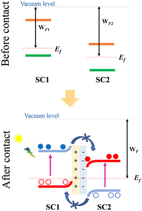
Within this framework, Z-scheme heterostructures have emerged as a promising subclass of Type-II band-aligned heterostructures, specifically designed to achieve efficient electron–hole separation with enhanced spatial separation. In these heterostructures, two 2D semiconductors with staggered (Type-II) band alignment are stacked to facilitate optimal charge separation. When the semiconductors combine to form a heterostructure, an initial charge transfer occurs between them, establishing a common Fermi level and resulting in a built-in electric field directed from the semiconductor with a lower work function and higher conduction band (denoted as SC1) toward the semiconductor with a higher work function (SC2) (Fig. 1).
Upon light exposure, electrons in each semiconductor become photoexcited, transitioning from the valence band (VB) to the conduction band (CB). The built-in electric field at the interface plays a critical role by preventing photoexcited electrons from relaxing into the lower conduction band of SC2 or holes from moving into the higher valence band of SC1. As a result, electrons remain confined to the conduction band of SC1, while holes accumulate in the valence band of SC2. This spatial separation across the two layers not only enhances charge separation but also reduces electron–hole recombination, significantly boosting the efficiency of the heterostructure for applications such as photocatalysis and photovoltaics.19,22 This is what necessitated the search for new Z-scheme heterostructures for this application, especially after the recent success in the fabrication of Z-scheme photocatalysts.23,24
Recently, a novel Z-scheme heterostructure for photovoltaic applications has been investigated, consisting of a CsPbBr3 surface and an SnS2 monolayer.25 This heterostructure has proven effective in efficiently separating (e–h) pairs, enhancing photovoltaic performance. Among heterostructures, two-dimensional (2D) semiconductors, prized for their tunable properties and high chemical stability, show great promise across various applications, particularly in optoelectronics and photovoltaics. Unlike traditional heterostructures, van der Waals heterostructures (vdWHs) composed of vertically or laterally stacked 2D monolayers offer unique advantages due to their weak interlayer interactions.26–32
The Germanium Carbide (GeC) monolayer, which has been successfully synthesized through experimental by chemical vapor deposition, has garnered increased interest from the scientific community.33 GeC exhibits a direct bandgap, and its electronic proprieties can be tuned around using several strategies, such as strain.34 GeC monolayer also entered into the formation of two-dimensional heterostructures such as GeC/MoSSe,35 GeC/SiC,36 GeC/BSe,37 blue phosphorus/GeC,38 GeC/ZnO.39 On the other hand, boron arsenide (BAs) has also drawn significant interest owing to its exceptional thermal conductivity and electronic properties, which have been thoroughly investigated in both bulk and two-dimensional structures.40–43 The heterostructures based on BAs monolayers have attracted considerable attention due to their potential in various applications, including optoelectronics and photocatalysis.44–47
Recently, Guo et al.48 used density functional theory (DFT) to explore three possible stacking configurations of the GeC/BAs heterostructure, selecting the most stable one based on calculated binding energy. Molecular dynamics simulations in their study showed a transition from one stacking arrangement to another, suggesting that the resulting configuration after simulation was the most stable. Conversely, Islam et al.49 identified a different stacking arrangement as the most stable. This difference in stacking led to a fundamental discrepancy: Guo et al.48 classified the BAs/GeC heterostructure as a Type-II heterostructure, while Islam et al.49 identified it as Type-I. Recognizing the importance of accurate band alignment in heterojunctions, we were motivated to further investigate the BAs/GeC heterostructure to determine its most stable stacking, especially given its promising electronic and optical properties for photovoltaic applications.
In this study, we construct a van der Waals heterostructure (vdWh) using BAs and GeC monolayers to develop an efficient Z-scheme system for solar energy applications. Using first-principles calculations, we investigate the geometric, electronic, and optoelectronic properties of the BAs/GeC vdWh across six different stacking configurations including the one previously studied.48,49 The binding energy for each configuration was determined using the HSE06 functional to accurately identify the most stable stacking. To further assess the stability of this optimal configuration, we performed phonon spectrum calculations and molecular dynamics simulations and evaluated their mechanical properties. Our study delves deeper into aspects that have not been previously covered, such as mechanical properties and Bader charge analysis. Indeed, we expanded the study to include a stability test under strain and we conducted a thorough investigation of the charge transfer mechanisms to confirm the presence of a Z-scheme heterostructure – a crucial feature not investigated in previous studies on the same heterostructure. We evaluated the optical absorption and resulting photovoltaic efficiency using two different methods to confirm the suitability of the BAs/GeC heterostructure for photovoltaic applications. Furthermore, we investigated the tunability of the bandgap and optical absorption properties of this heterostructure under biaxial strain.
2 Computational details
In this study, we performed first-principles calculations using the Vienna Ab initio Simulation Package (VASP.6.3).50,51 We employed the Perdew–Burke–Ernzerhof (PBE) generalized gradient approximation (GGA) for the exchange–correlation functional and utilized the projector augmented wave (PAW) method to account for ion–electron interactions.52–54 The optimization of K-points sampling and cutoff energy was carried out to ensure accuracy in the results. K-points grill convergence was tested from 6 × 6 × 1 to 18 × 18 × 1 at intervals of 3 × 3 × 1, converging at 15 × 15 × 1. The kinetic energy cutoff (ecut) convergence was tested in the range from 200 to 600 eV at intervals of 50 eV, converging at 500 eV (see Fig. S1†). All calculations were then performed using the converged values of the K-points and cutoff energy. Atomic positions were relaxed with a force criterion of 0.01 eV Å−1 and an energy conversion criterion of 10−7 eV. A vacuum space of 25 Å was incorporated along the z direction to prevent potential interaction between the periodic images of the monolayers. van der Waals interactions were included using the Becke–Johnson damping method (DFT-D3) coupled with Grimme dispersion correction.55 To accurately characterize the electronic and optical properties of the system, we also used the Heyd–Scuseria–Ernzerhof hybrid functional (HSE06).56 Dynamic stability was assessed through phonon spectra calculations. The phonon calculations were performed using density functional perturbation theory (DFPT) on a 2 × 2 × 1 supercell, adhering to strict convergence criteria of 10−9 eV.57 The phonon spectra were subsequently generated by processing the atomic forces with the PHONOPY code.58,59 Thermal stability was evaluated through ab initio molecular dynamics (AIMD) simulations at 300 K and 500 K using the Nose thermostat algorithm over 5 picoseconds with a time step of 1 femtosecond.60,61 The results calculated by VASP are post-processed using the VASPKIT program, and the structure and charge density difference visualizations are created with VESTA.62,633 Results and discussion
3.1 Geometric structures and stabilities of BAs/GeC heterostructure
Our investigation begins with a comprehensive examination of the structural and electronic properties of individual BAs and GeC monolayers. Both monolayers exhibit a planar hexagonal structure, characterized by lattice parameters of 3.38 and 3.26 Å for BAs and GeC, respectively (see Fig. 2). Each monolayer behaves as a direct bandgap semiconductor when examining the electronic properties. Specifically, using the GGA-PBE (HSE06) functional, we find bandgaps of 0.75 eV (1.180 eV) and 2.06 eV (2.89 eV) for the BAs and GeC monolayers, respectively. Our results are consistent with previous studies.64–68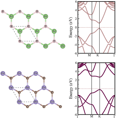 | ||
| Fig. 2 The left panel illustrates the crystal structures of the isolated BAs and GeC monolayers, and the right panel presents their electronic band structures. | ||
The lattice mismatch between BAs and GeC monolayers is 3.75% (less than 5.00%), indicating a suitable condition for the construction of the BAs/GeC heterostructure.69
We then constructed vdW heterostructures by placing a GeC monolayer on top of a BAs monolayer. We investigate six possible stacking configurations, labeled AA, AA′, AB (boron), AB (arsenic), AB′ (boron) and AB′ (arsenic), as shown in Fig. 3. In the first four configurations, the GeC monolayer atoms are positioned at (0, 0) for carbon (C) atoms and at (1/3, 2/3) for germanium (Ge) atoms. In AA-stacking, a Ge atom is above an As atom, and a C atom is above a B atom. In AA′-stacking, the positions are reversed, with a C atom above an As atom and a Ge atom above a B atom. In AB (boron)-stacking, a Ge atom is above a B atom, with a hollow site above the As atom. Similarly, in AB (arsenic)-stacking, a Ge atom is located above an As atom, with a hollow position above the B atom. In AB′ (arsenic) stacking, a C atom is above an As atom, with a hollow site above the B atom. The positions in AB′ (boron)-stacking are reversed, with a C atom above a B atom and a hollow site above the As atom.
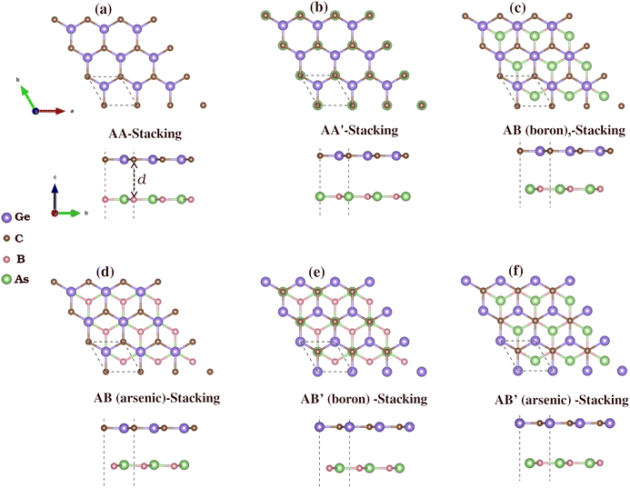 | ||
| Fig. 3 Top and side views of the six different possible stacking configurations of BAs/GeC heterostructure, labeled (a–f). (For more details, see the text). | ||
We calculated the binding energies (Eb) to confirm the energy stability of the six stacking configurations. The Eb is defined as:
| Eb = EBAs/GeC − (EBAs + EGeC) | (1) |
| System | a (Å) | dinter (Å) | Eb (eV) |
|---|---|---|---|
| AA-stacking | 3.308 | 4.004 | −0.238 |
| AA′-stacking | 3.307 | 4.090 | −0.227 |
| AB (boron)-stacking | 3.307 | 3.614 | −0.287 |
| AB (arsenic)-stacking | 3.307 | 3.501 | −0.295 |
| AB′ (boron)-stacking | 3.306 | 3.939 | −0.239 |
| AB′ (arsenic)-stacking | 3.308 | 3.793 | −0.255 |
To confirm the dynamic and thermal stability of our heterostructure, we conducted phonon spectra analysis and ab initio molecular dynamics (AIMD) calculations. The phonon spectra (Fig. 3) show no imaginary frequencies, indicating that the BAs/GeC heterostructure is dynamically stable. AIMD simulations were performed at room temperature and 500 K, with a total simulation time of 5000 fs. The results indicate that the thermal fluctuations are limited to a narrow range, and no bond breaking or structural transitions were observed upon heating (Fig. 4). These results support the high thermal stability of the BAs/GeC heterostructures at room temperature and elevated temperatures up to 500 K.
Additionally, we employed the stress–strain method with finite differences of 0.020 Å to determine the elastic constants Cij of the BAs/GeC heterostructure to evaluate their mechanical stability under in-plane strain.70 Given the hexagonal structure of these heterostructures, it was necessary to compute only two independent constants, C11 and C12 with C66 derived using the relation C66 = (C11 − C12)/2. The obtained values for C11 and C12 are 283.108 N m−1 and 85.790 N m−1, respectively. The conditions C11 > 0 and C11 > C12 validate the intrinsic mechanical stability of the heterostructure.71 Young's modulus Y, a crucial parameter indicating the material's stiffness and its deformation response to stress, is calculated using the formula:72
Our calculations show that Young's modulus for the BAs/GeC heterostructure is approximately 184.45 GPa. Compared to the individual BAs (116.27 GPa) and GeC (102.19 GPa) monolayers, the BAs/GeC heterostructure exhibits superior mechanical performance due to its higher Young's modulus. These results indicate an improvement in mechanical stability and rigidity of the heterostructure, highlighting its potential for advanced materials applications.
To calculate Poisson's ratio (ν), the lateral expansion is measured relative to the longitudinal compression, using the following formula:72
A Poisson's ratio of 0.303 was determined for our heterostructure, indicating a remarkable degree of ductility. The combination of hardness and ductility makes this heterostructure suitable for applications requiring durable and flexible materials.
Our comprehensive evaluation of various stability factors provides strong evidence for the stability of the BAs/GeC heterostructure. This opens the way for a more in-depth exploration of its various physical properties and supports the practical feasibility of experimentally implementing this van der Waals heterostructure.
3.2 Electronic properties of BAs/GeC van der Waals heterostructure
To understand the electronic properties of the studied van der Waals heterostructure (vdWh), we calculated the band structures and the density of states for the BAs/GeC vdWh using HSE06 functions (Fig. 5). Our results indicate that the heterostructure is a direct bandgap semiconductor, with the valence band maximum (VBM) and conduction band minimum (CBM) both located at the K point within the Brillouin zone. The calculated bandgap energy (Eg) for the BAs/GeC heterostructure is 1.05 eV. Considering the results of the two previous studies, the electronic properties in the first paper were calculated only with the PBE functional, yielding a band gap of 0.19 eV, without using hybrid functionals (HSE).48 In contrast, the second study reported a band gap of 1.74 eV using HSE.49 This significant difference in band gap values is attributed to the variation in stacking configurations.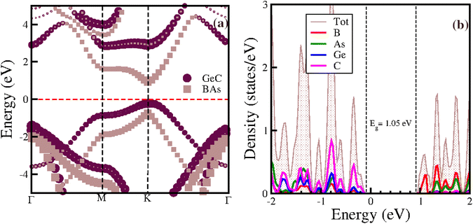 | ||
| Fig. 5 (a) Electronic band structure and (b) projected density of states of the BAs/GeC heterostructure. | ||
Fig. 5(a) displays the projected band structure of the BAs and GeC monolayers within the BAs/GeC heterostructure. The results reveal that the maximum valence band (VBM) primarily originates from the GeC monolayer, while the minimum of the conduction band (CBM) is mainly derived from the BAs monolayer. This distinct configuration signifies Type-II band alignment. This observation is further corroborated by the projected density of states (PDOS) shown in Fig. 5(b), where it is evident that the carbon (C) states contribute significantly to the VBM. At the same time, the conduction band minimum is predominantly composed of boron (B) and arsenic (As) states. These properties highlight the potential of the BAs/GeC heterostructure as a promising candidate for developing high-performance photovoltaic and optoelectronic devices.73
The formation of heterostructures often involves significant electron transfer and interfacial redistribution caused by differences in atomic electronegativity between individual layers. To accurately evaluate the mechanism of charge transfer qualitatively, the charge density difference (Δρ) along the z-direction is calculated using the following equation:
| Δρ = ρBAs/GeC − ρBAs − ρGeC | (2) |
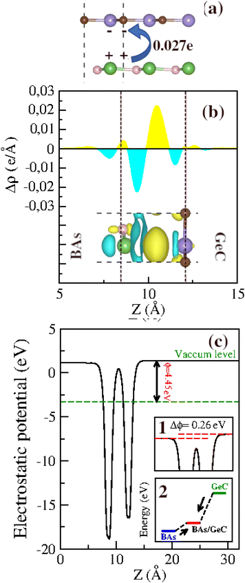
Before exploring the band alignment of heterostructures, it is crucial to understand how electrons flow and how Fermi energy levels shift during their formation. The difference in work function between the two monolayers forming the heterostructure is necessary for creating a built-in electric field. The work functions of the BAs monolayer, the GeC monolayer, and the BAs/GeC vdWH were calculated to be 4.91 eV, 2.81 eV, and 4.45 eV, respectively. The work function of the BAs/GeC vdWH falls between those of the individual BAs and GeC monolayers. When the GeC monolayer comes into contact with the BAs monolayer, electrons flow from GeC to BAs due to GeC's lower work function. As electrons are transferred, the Fermi energy level of BAs rises, while the Fermi energy level of GeC decreases until they reach an equilibrium energy level (Fig. 6(c)).2 This electron transfer results in a built-in electric field directed from the GeC monolayer to the BAs monolayer, which could plays a crucial role in the efficient separation and dynamic of photogenerated carriers within the heterostructure.
Fig. 6(c) illustrates the electrostatic potential along the z-axis of the BAs/GeC vdWh. In its optimized form, this heterostructure shows a difference in electrostatic potential energy, with the BAs monolayer having a lower potential than the GeC monolayer. This indicates an interfacial built-in electric field extending from the GeC monolayer towards the BAs monolayer at the heterostructure interface. This built-in electric field reduces carrier recombination rates and increases carrier lifetimes. As a result, it is essential to study the electron transfer within the heterostructure and the impact of this built-in electric field on it. Fig. 7 presents a schematic depiction of the band alignment and the migration behavior of photogenerated carriers at the BAs/GeC interface. The analysis of the conduction band offset (ΔEc) and valence band offset (ΔEv) between the BAs and GeC layers shows values of 1.69 eV and 0.25 eV, respectively.
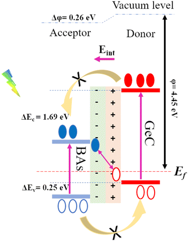 | ||
| Fig. 7 Schematic representation of the Z-scheme band alignment, including the movement of electrons (filled circles) and holes (empty circles). | ||
When exposed to light, electrons in both the BAs and GeC monolayers are excited from the valence band to the conduction band, forming electron–hole pairs. It was initially expected that electrons would migrate from the conduction band of the GeC monolayer (acting as the donor) to the conduction band of the BAs monolayer (acting as the acceptor). Simultaneously, it was anticipated that holes would move from the valence band of the BAs monolayer to the valence band of the GeC monolayer. This expectation stems from the principle that electrons tend to migrate to lower energy states, while holes prefer higher energy states, which is a behavior characteristic of a Type-II heterostructure.
However, the actual outcome differed from this expectation. The built-in electric field (Eint) and the subsequent band bending, created due to the heterostructure's formation and oriented from the GeC monolayer towards the BAs monolayer, impedes the transfer of electrons from the GeC monolayer to the BAs monolayer and the transfer of holes from the BAs monolayer to the GeC monolayer. As a result, electrons accumulate in the conduction band of the GeC monolayer, while holes gather in the valence band of the BAs monolayer. This accumulation of charge carriers confirms that the BAs/GeC heterostructure operates via a Z-scheme charge transfer pathway. This specific band alignment configuration effectively reduces the rate of electron–hole recombination and prolongs the lifetimes of photogenerated carriers. These characteristics make the BAs/GeC heterostructure a promising candidate for high-efficiency solar cell applications, as it enhances the separation and utilization of photogenerated charge carriers.
3.3 Effect of the biaxial strains on BAs/GeC heterostructure
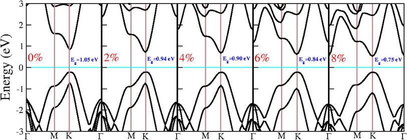
Strain can significantly influence the electronic and optical properties of semiconductors, thereby altering their behaviour. As a result, it is widely recognized as an effective method for modulating the properties of 2D materials. When these heterostructures are used as active layers in solar cell devices, the strain induced by lattice mismatch with other device layers may affect their performance. The following section delves into the impact of strain on the electronic and optical properties of the BAs/GeC heterostructure, exploring how these properties can be tuned to optimize device performance.Biaxial strain (ε) is defined as ε = (a − a0)/a0, where a and a0 represent the strained and unstrained lattice constants, respectively. Although many studies suggest that most 2D materials can withstand stretchability up to 20% without structural failure, we applied a biaxial strain ranging from −8% to 8%, with increments of 2% to ensure rationality and simplicity in our analysis. We analyzed the phonon dispersion at each applied strain level to assess the BAs/GeC heterostructure's susceptibility to strain. Fig. 8 shows the obtained results.
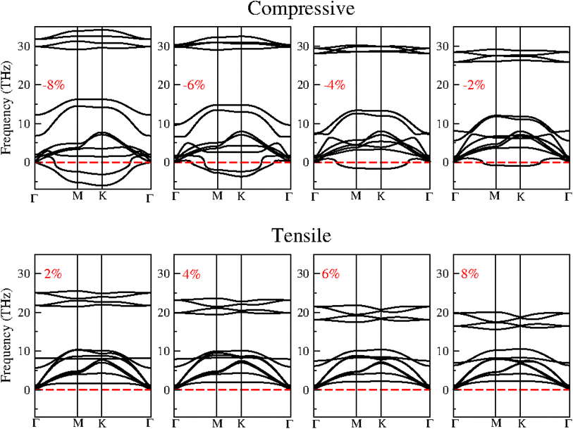 | ||
| Fig. 8 The phonon dispersion of BAs/GeC heterostructure with applied biaxial compressive and tensile strain ranging from −8% to 8%. | ||
The presence of imaginary frequencies in the phonon spectra under compressive strain indicates instability, while their absence under tensile strain suggests stability. This demonstrates that the BAs/GeC heterostructure is stable only under tensile strain. Therefore, our study focuses exclusively on tensile structures to investigate the effect of strain on the electronic and optical properties of the BAs/GeC heterostructure. Using the HSE06 functional, we calculated the tensile structure bandgaps, illustrating the bandgap variation with applied biaxial strain in Fig. 9. The BAs/GeC heterostructure maintains a direct bandgap under biaxial tensile strain, decreasing from 1.05 eV at 0% strain to 0.75 eV at 8% strain. These changes can be attributed to strain-induced alterations in the band structures of the individual materials, interfacial distances, and interlayer couplings.
3.4 Optical properties and power conversion efficiency
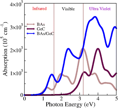
Considering that optical properties are crucial indicators in evaluating materials for solar energy conversion applications, we investigated the optical absorption coefficient of BAs/GeC heterostructures using HSE06 functional, following the formula:75
 | (3) |
We investigated also the optical absorption coefficients influenced by strain engineering. Fig. S2† illustrates the optical absorption under various tensile biaxial strains, the absorption intensity of the heterostructure is slightly higher under 2% and 4% biaxial tensile strain compared to 0% strain at 1.5 eV. However, it decreases under 6% and 8% biaxial tensile strain. Under tensile strain, the material exhibits small redshifts in absorption at 6% and 8% biaxial strain, indicating a shift towards lower-energy absorption peaks. However, as the strain increases, the material's efficiency begins to decrease. This reduction in efficiency can be attributed to the strain-induced alterations in the electronic structure, which may lead to a weakening of light absorption. Therefore, while moderate tensile strain can slightly affect the absorption characteristics, excessive strain negatively impacts the material's overall performance.
To evaluate the photovoltaic efficiency of the BAs/GeC heterostructure, the Power Conversion Efficiency (PCE) was calculated using the Scharber method according to the following formula:76
 | (4) |
The findings reveal a remarkable PCE for the BAs/GeC heterostructure, clocking in at approximately 30.58%. This is an outstanding achievement, surpassing previous heterostructures such as black-P/blue-P (20.25%)77 and BP/SnSe (17.24%)78 by a significant margin.
4 Conclusion
BAs/GeC van der Waals heterostructure exhibit robust stability, suitable bandgap, Type-II band alignment, high-performance optical absorption, and significant photoresponsiveness. The built-in electric field resulting from charge transfer between the BAs and GeC monolayers effectively suppresses the recombination of electron–hole pairs generated by light, enhancing photovoltaic efficiency. The enhanced absorption intensity of the vdW heterostructures, compared to their individual monolayers, enables more efficient utilization of visible light. Additionally, functioning as a direct Z-scheme heterostructure, BAs/GeC vdWHs achieve a high power conversion efficiency of up to 31%, representing a notable advancement in heterostructure performance. Further investigation indicates that both the bandgap and optical absorption properties can be tuned by applying biaxial strains. However, the BAs/GeC vdWH exhibits dynamic instability under compressive biaxial strain, prompting our study to focus exclusively on biaxial tensile strain. Under tensile strain, although small redshifts in absorption occur at 6% and 8% biaxial strain, the material's efficiency decreases as the strain increases. These findings underscore the significant potential of BAs/GeC vdWHs for advancing high-efficiency solar cell technology. Their unique combination of stability, optical properties, and efficiency enhancements positions them as promising candidates for future photovoltaic applications.Data availability
The data that support the findings of this study are available from the corresponding author upon reasonable request.Author contributions
Khawla Chaoui: conceptualization, formal analysis, data curation, investigation, software, visualization, writing – original draft. Kamel Zanat: supervision, investigation, validation. Warda Elaggoune: methodology, investigation, review & editing. Luc Henrard: analyzed the results and finalized the manuscript. Mohamed Achehboune: supervision, resources, formal analysis, writing – review & editing.Conflicts of interest
There are no conflicts to declare.Acknowledgements
This research used resources of the “Consortium des Équipements de Calcul Intensif (CÉCI)”, funded by the Fonds de la Recherche Scientifique de Belgique (F. R. S.-FNRS) and the Wallon region (Conventions No. 2.5020.11, GEQ U.G006.15, 1610468, RW/GEQ2016 et U.G011.22).References
- P. K. Ozili and E. Ozen, The Impact of Climate Change and Sustainability Standards on the Insurance Market, 2023, pp. 439–454 Search PubMed.
- D. Gielen, F. Boshell, D. Saygin, M. D. Bazilian, N. Wagner and R. Gorini, Energy Strategy Rev., 2019, 24, 38–50 CrossRef.
- Q. Hassan, P. Viktor, T. J. Al-Musawi, B. M. Ali, S. Algburi, H. M. Alzoubi, A. K. Al-Jiboory, A. Z. Sameen, H. M. Salman and M. Jaszczur, Renewable Energy Focus, 2024, 48, 100545 CrossRef.
- Z. Caineng, M. Feng, P. Songqi, Z. Qun, F. Guoyou, G. Zhang, Y. Yichao, Y. Hao, Y. Liang and L. Minjie, et al., Pet. Explor. Dev., 2023, 50, 722–740 CrossRef.
- N. Mariotti, M. Bonomo, L. Fagiolari, N. Barbero, C. Gerbaldi, F. Bella and C. Barolo, Green Chem., 2020, 22, 7168–7218 RSC.
- C. G. Granqvist, Adv. Mater., 2003, 15, 1789–1803 CrossRef CAS.
- M. Green, in Third Generation Photovoltaics: Advanced Solar Energy Conversion, Springer Berlin Heidelberg, Berlin, Heidelberg, 2003, pp. 21–34 Search PubMed.
- N.-G. Park, M. Grätzel, T. Miyasaka, K. Zhu and K. Emery, Nat. Energy, 2016, 1, 1–8 Search PubMed.
- W. Zhang, C. Chai, Q. Fan, Y. Song and Y. Yang, Results Phys., 2020, 18, 103271 CrossRef.
- O. J. Sandberg, A. Sundqvist, M. Nyman and R. Österbacka, Phys. Rev. Appl., 2016, 5, 044005 CrossRef.
- S. De Wolf, J. Holovsky, S.-J. Moon, P. Loper, B. Niesen, M. Ledinsky, F.-J. Haug, J.-H. Yum and C. Ballif, J. Phys. Chem. Lett., 2014, 5, 1035–1039 CrossRef CAS PubMed.
- Y. Peter and M. Cardona, Fundamentals of Semiconductors: Physics and Materials Properties, Springer Science & Business Media, 2010 Search PubMed.
- A. Polman, M. Knight, E. C. Garnett, B. Ehrler and W. C. Sinke, Science, 2016, 352, aad4424 CrossRef PubMed.
- M. A. Green, A. Ho-Baillie and H. J. Snaith, Nat. Photonics, 2014, 8, 506–514 CrossRef CAS.
- H. Kroemer, Rev. Mod. Phys., 2001, 73, 783–793 CrossRef CAS.
- A. K. Geim and I. V. Grigorieva, Nature, 2013, 499, 419–425 CrossRef PubMed.
- F. Withers, O. Del Pozo-Zamudio, A. Mishchenko, A. P. Rooney, A. Gholinia, K. Watanabe, T. Taniguchi, S. J. Haigh, A. Geim and A. Tartakovskii, et al., Nat. Mater., 2015, 14, 301–306 CrossRef PubMed.
- L. Song, M. Song, Z. Lu, G. Yu, Z. Liang, W. Hou, Q. Liao and Y. Song, Coatings, 2022, 12, 1152 CrossRef.
- F. Yu, Y. Zhou, J. Cui, Z. Liu, Y. Li, L. He, J. Zhang, X. Tang and Y. Liu, J. Mater. Sci., 2022, 57, 983–1005 CrossRef.
- Y. Guan, X. Li, Q. Hu, D. Zhao and L. Zhang, Appl. Surf. Sci., 2022, 599, 153865 CrossRef.
- S. E. Tsoeu, F. Opoku and P. P. Govender, SN Appl. Sci., 2020, 2, 341 CrossRef.
- S. Li, W. Xu, L. Meng, W. Tian and L. Li, Small Sci., 2022, 2, 2100112 CrossRef.
- Z. Li, J. Hou, B. Zhang, S. Cao, Y. Wu, Z. Gao, X. Nie and L. Sun, Nano Energy, 2019, 59, 537–544 CrossRef.
- X. Liu, Q. Zhang and D. Ma, Sol. RRL, 2021, 5, 2000397 CrossRef.
- M. Zhang, Y. Lin, J. Li, X. Wei, Y. Peng, Z. Wang, V. Maheskumar, Z. Jiang and A. Du, J. Mater. Chem. A, 2023, 11, 4758–4768 RSC.
- F. Withers, O. Del Pozo-Zamudio, A. Mishchenko, A. P. Rooney, A. Gholinia, K. Watanabe, T. Taniguchi, S. J. Haigh, A. Geim and A. Tartakovskii, et al., Nat. Mater., 2015, 14, 301–306 CrossRef PubMed.
- K. S. Novoselov, A. Mishchenko, A. Carvalho and A. Castro Neto, Science, 2016, 353, aac9439 CrossRef.
- A. Bakhtatou, A. Hamidani, K. Zanat, Y. O. Ciftci, I. K. Durukan and F. Ersan, J. Phys. Chem. Solids, 2023, 183, 111654 CrossRef.
- P. K. Sahoo, S. Memaran, Y. Xin, L. Balicas and H. R. Gutiérrez, Nature, 2018, 553, 63–67 CrossRef PubMed.
- Y.-C. Rao, S. Yu and X.-M. Duan, Phys. Chem. Chem. Phys., 2017, 19, 17250–17255 RSC.
- X. Hong, J. Kim, S.-F. Shi, Y. Zhang, C. Jin, Y. Sun, S. Tongay, J. Wu, Y. Zhang and F. Wang, Nat. Nanotechnol., 2014, 9, 682–686 CrossRef PubMed.
- Q. Zheng, W. A. Saidi, Y. Xie, Z. Lan, O. V. Prezhdo, H. Petek and J. Zhao, Nano Lett., 2017, 17, 6435–6442 CrossRef PubMed.
- F. Sousani, H. Jamali, R. Mozafarinia and A. Eshaghi, Infrared Phys. Technol., 2018, 93, 255–259 CrossRef.
- Y. Ji, H. Dong, T. Hou and Y. Li, J. Mater. Chem. A, 2018, 6, 2212–2218 RSC.
- H. Din, M. Idrees, A. Albar, M. Shafiq, I. Ahmad, C. V. Nguyen and B. Amin, Phys. Rev. B, 2019, 100, 165425 CrossRef.
- M. R. Islam, M. S. Islam, A. F. Mitul, M. R. H. Mojumder, A. J. Islam, C. Stampfl and J. Park, Sci. Rep., 2021, 11, 17739 CrossRef PubMed.
- X. Huang, Z. Cui, X. Shu, H. Dong, Y. Weng, Y. Wang and Z. Yang, Phys. Rev. Mater., 2022, 6, 034010 CrossRef.
- X. Gao, Y. Shen, Y. Ma, S. Wu and Z. Zhou, Appl. Phys. Lett., 2019, 114, 093902 CrossRef.
- G. Wang, L. Zhang, Y. Li, W. Zhao, A. Kuang, Y. Li, L. Xia, Y. Li and S. Xiao, J. Phys. D: Appl. Phys., 2019, 53, 015104 CrossRef.
- J. S. Kang, M. Li, H. Wu, H. Nguyen and Y. Hu, Appl. Phys. Lett., 2019, 115, 122103 CrossRef.
- J. S. Kang, M. Li, H. Wu, H. Nguyen and Y. Hu, Science, 2018, 361, 575–578 CrossRef PubMed.
- Y. Hu, D. Li, Y. Yin, S. Li, H. Zhou and G. Zhang, RSC Adv., 2020, 10, 25305–25310 RSC.
- R. Islam, S. Islam, R. H. Mojumder, Z. Khan, H. Molla, A. J. Islam and J. Park, Mater. Today Commun., 2022, 33, 104227 CrossRef.
- K. Bushick, S. Chae, Z. Deng, J. T. Heron and E. Kioupakis, npj Comput. Mater., 2020, 6, 3 CrossRef.
- D. Wei, E. Zhou, J. Xu, A. Chen, H. Xie, F. Duan, H. Wang, Z. Qin and G. Qin, Phys. Rev. B, 2024, 109, 205408 CrossRef.
- G. Xiong, J. Lu, R. Wang, Z. Lin, S. Lu, J. Li, Z. Tong, Z. Qiu, K. Chen and Y. Sun, et al., Mater. Today Phys., 2024, 42, 101360 CrossRef.
- Y. He and H. Sun, Phys. Rev. Mater., 2022, 6, 034603 CrossRef.
- R. Guo, L. Luan, M. Cao, Y. Zhang, X. Wei, J. Fan, L. Ni, C. Liu, Y. Yang and J. Liu, et al., Phys. E, 2023, 149, 115628 CrossRef.
- M. R. Islam, M. S. Islam, M. Y. Zamil, N. Ferdous, C. Stampfl, J. Park and M. K. Hossain, J. Phys. Chem. Solids, 2023, 176, 111263 CrossRef.
- G. Kresse and J. Hafner, Phys. Rev. B: Condens. Matter Mater. Phys., 1993, 48, 13115 CrossRef CAS.
- G. Kresse and J. Furthmüller, Phys. Rev. B: Condens. Matter Mater. Phys., 1996, 54, 11169 CrossRef CAS PubMed.
- M. Ernzerhof and G. E. Scuseria, J. Chem. Phys., 1999, 110, 5029–5036 CrossRef CAS.
- S. Grimme, J. Comput. Chem., 2006, 27, 1787–1799 CrossRef CAS.
- P. E. Blöchl, Phys. Rev. B: Condens. Matter Mater. Phys., 1994, 50, 17953 CrossRef PubMed.
- S. Grimme, S. Ehrlich and L. Goerigk, J. Comput. Chem., 2011, 32, 1456–1465 CrossRef CAS.
- J. Heyd, G. E. Scuseria and M. Ernzerhof, J. Chem. Phys., 2003, 118, 8207–8215 CrossRef CAS.
- L. Chaput, A. Togo, I. Tanaka and G. Hug, Phys. Rev. B: Condens. Matter Mater. Phys., 2011, 84, 094302 CrossRef.
- A. Togo, L. Chaput, T. Tadano and I. Tanaka, J. Phys.: Condens. Matter, 2023, 353001 CrossRef CAS PubMed.
- A. Togo, J. Phys. Soc. Jpn., 2023, 92, 012001 CrossRef.
- S. Nosé, Mol. Phys., 1984, 52, 255–268 CrossRef.
- W. G. Hoover, Phys. Rev. A, 1985, 31, 1695 CrossRef.
- V. Wang, N. Xu, J.-C. Liu, G. Tang and W.-T. Geng, Comput. Phys. Commun., 2021, 267, 108033 CrossRef CAS.
- K. Momma and F. Izumi, J. Appl. Crystallogr., 2008, 41, 653–658 CrossRef.
- Z. Lu, S. Jia, G. Li, P. Sun, S. Jiang, Y. Cao, J. Li and S. Jing, Mater. Sci. Semicond. Process., 2024, 173, 108163 CrossRef.
- S. Ahmad, H. Din, S. U. Sabir and B. Amin, Nanoscale Adv., 2023, 5, 4598–4608 RSC.
- S. Ahmad, K. Sohail, L. Chen, H. Xu, H. Din and Z. Zhou, Int. J. Hydrogen Energy, 2023, 25354–25365 CrossRef.
- J. Yang, C. Chen, J. Zhang, W. Zhou, H. Qu, J. Li, T. Guo, X. Shi, Z. Wu and S. Zhang, Adv. Electron. Mater., 2022, 8, 2200388 CrossRef.
- G. Wang, L. Zhang, Y. Li, W. Zhao, A. Kuang, Y. Li, L. Xia, Y. Li and S. Xiao, J. Phys. D: Appl. Phys., 2019, 53, 015104 CrossRef.
- H. Zheng, X.-B. Li, N.-K. Chen, S.-Y. Xie, W. Q. Tian, Y. Chen, H. Xia, S. Zhang and H.-B. Sun, Phys. Rev. B: Condens. Matter Mater. Phys., 2015, 92, 115307 CrossRef.
- M. Born and K. Huang, Dynamical Theory of Crystal Lattices, Oxford university press, 1996 Search PubMed.
- V. Wang, G. Tang, Y.-C. Liu, R.-T. Wang, H. Mizuseki, Y. Kawazoe, J. Nara and W. T. Geng, J. Phys. Chem. Lett., 2022, 13, 11581–11594 CrossRef PubMed.
- R. C. Andrew, R. E. Mapasha, A. M. Ukpong and N. Chetty, Phys. Rev. B: Condens. Matter Mater. Phys., 2012, 85, 125428 CrossRef.
- P. Rivera, K. L. Seyler, H. Yu, J. R. Schaibley, J. Yan, D. G. Mandrus, W. Yao and X. Xu, Science, 2016, 351, 688–691 CrossRef PubMed.
- G. Henkelman, A. Arnaldsson and H. Jónsson, Comput. Mater. Sci., 2006, 36, 354–360 CrossRef.
- M. Gajdoš, K. Hummer, G. Kresse, J. Furthmüller and F. Bechstedt, Phys. Rev. B: Condens. Matter Mater. Phys., 2006, 73, 045112 CrossRef.
- M. C. Scharber, D. Mühlbacher, M. Koppe, P. Denk, C. Waldauf, A. J. Heeger and C. J. Brabec, Adv. Mater., 2006, 18, 789–794 CrossRef CAS.
- T. Wen, Y. Yang and J. Li, Chem. Phys. Lett., 2023, 812, 140242 CrossRef CAS.
- W. Dou, A. Huang, Y. Ji, X. Yang, Y. Xin, H. Shi, M. Wang, Z. Xiao, M. Zhou and P. K. Chu, Phys. Chem. Chem. Phys., 2020, 22, 14787–14795 RSC.
Footnote |
| † Electronic supplementary information (ESI) available. See DOI: https://doi.org/10.1039/d4ra08369e |
| This journal is © The Royal Society of Chemistry 2024 |

