
Surface-deprotonated ultra-small SnO2 quantum dots for high-performance perovskite solar cells†
Wuchen
Xiang‡
ac,
Yiheng
Gao‡
a,
Bobo
Yuan
a,
Shuping
Xiao
a,
Rui
Wu
a,
Yiran
Wan
a,
Zhiqiang
Liu
c,
Liang
Ma
 a,
Xiangbai
Chen
a,
Weijun
Ke
b,
Guojia
Fang
b and
Pingli
Qin
*a
a,
Xiangbai
Chen
a,
Weijun
Ke
b,
Guojia
Fang
b and
Pingli
Qin
*a
aHubei Key Laboratory of Optical Information and Pattern Recognition, Wuhan Institute of Technology, Wuhan, Hubei 430205, P. R. China. E-mail: qpl2015@wit.edu.cn
bSchool of Physics and Technology, Key Laboratory of Artificial Micro- and Nano-structures of the Ministry of Education and School of Physics and Technology, Wuhan University, Wuhan 430072, P. R. China
cWuhan National Laboratory for Optoelectronics and School of Optical and Electronic Information, Huazhong University of Science and Technology, Wuhan, 430074, P. R. China
First published on 12th November 2024
Abstract
SnO2 electron transport layers (ETLs) have significantly boosted the recent record efficiencies in perovskite solar cells (PSCs). However, solution-processed SnO2 ETLs often suffer from surface protonation with interface/surface defects, leading to substantial energy loss and interface instability. Herein, we investigated the surface properties of SnO2 quantum dots (QDs) on device performance and then developed surface-deprotonated ultra-small SnO2 QD ETLs. Our findings revealed that traditional SnO2 QDs with thiourea doping introduced surface positive-charge protonation to recombine transferred electrons and lengthen their migration path, thereby reducing the electron-transfer efficiency and increasing the surface photocatalytic activity. In contrast, our surface-deprotonated ultra-small SnO2 QDs (2.5 nm average size) exhibited effective coordination between PbI2 and SnO2, lowering the interface barrier and suppressing carrier accumulation for rapid electron transfer and extraction. Consequently, PSCs with non-protonated SnO2 QDs as ETLs achieved a significantly improved champion PCE of 25.55% and enhanced stability, outperforming those with the protonated SnO2 QD ETLs. The corresponding X-ray detector devices also demonstrate broad applicability for superior detection performance.
Broader contextSnO2 electron transport layers (ETLs) have significantly boosted recent record efficiencies in perovskite solar cells (PSCs). However, solution-processed SnO2 ETLs often suffer from surface protonation with interface/surface defects, leading to substantial energy loss and interface instability. Herein, we have investigated the surface properties of SnO2 quantum dots (QDs) on device performance and then developed surface-deprotonated ultra-small SnO2 QD ETLs. Our findings reveal that traditional SnO2 QDs with thiourea doping introduced surface positive-charge protonation to recombine transferred electrons and lengthen its migration path, thereby reducing the electron-transfer efficiency and increasing surface photocatalytic activity. In contrast, our surface-deprotonated ultra-small SnO2 QDs (2.5 nm average size) exhibit effective coordination between PbI2 and SnO2, lowering the interface barrier and suppressing carrier accumulation for rapid electron transfer and extraction. Consequently, PSCs with non-protonated SnO2 QDs as ETLs achieved a significantly improved champion PCE of 25.55% and enhanced stability, outperforming those with protonated SnO2 QD ETLs. The corresponding X-ray detector devices also demonstrate broad applicability for superior detection performance. |
Introduction
To address the impending energy crisis, photovoltaic (PV) power generation technology has garnered significant attention for its ability to convert solar energy into clean and usable power. Among various PV technologies, perovskite solar cells (PSCs) have emerged as highly promising devices due to their long carrier transport path,1–4 high absorption coefficient,5,6 and adjustable bandgap.7–10 Currently, more attention has been focused on the surface/interface defects, including the buried/front interface that are related to electron transport layers (ETLs)/hole transport layers (HTLs), respectively, which can impact the carrier dynamics process and stability at the interface.11 For common tin dioxide (SnO2) ETLs, many scholars have adopted various strategies to achieve excellent properties with high native mobility (ca. 421 cm2 V−1 s−1),12 excellent visible light transmittance (ca. 3.6 eV), good anti-reflection, decent chemical stability, low sintering temperature, good valence band maximum and energetic compatibility with perovskites.13–16 Therefore, it has become an outstanding component as ETL in n–i–p PSCs with high performance, thereby bringing record power conversion efficiencies (PCEs).17–19Generally, the solution method is a common and low-cost method for preparing SnO2 ETLs. However, the insufficient combustion reaction at low annealing temperatures (below 200 °C) can induce several valence states of tin, along with some intrinsic defects (e.g., oxygen vacancy and surface dangling states) in the bulk, at grain boundaries (GBs) or on the surface of the SnO2 film.20 Specifically, surface dangling states have been killer defects in the amorphous state that can cause an SnO2 energy level mismatch with perovskite. This can make the related interface prone to some severe problems, such as high resistance and non-radiative recombination.21–25 SnO2 has a relatively weak light absorption in the visible range. However, its absorption edge is located in the ultraviolet region,26 which triggers the surface photocatalytic activity for the unstable interface between SnO2 and perovskites. High-temperature annealing (∼500 °C) can achieve a well-crystallized SnO2, thereby decreasing its intrinsic defects, but this increases the additional costs along with sacrificing the electron-transport performance.22 Therefore, some functionalization capping agents are expected to conquer these inherent surface defects to weaken the catalytic activity,8 as well as to optimize the energy level arrangement with adjacent functional layers for the smooth charge transport process.26–31 Although introducing the narrow bandgap neighbors enhances light absorption,8 these foreign bodies make the SnO2 surface protonated,32–36 introducing some new defects for the enhanced surface/interface catalytic activity, which not only prematurely recombines the transferred electron, but also lengthens the electron migration path to decay the electron transfer among SnO2 quantum dots (QDs) or between SnO2 QDs and perovskite for the improved hysteresis phenomenon in PSC devices.
Besides the amorphous and crystalline state, SnO2 QDs, with the size of the nanoparticles equal to or smaller than the exciton Bohr radius (ca. 2.7 nm),37 exhibit high surface-to-volume ratio,38 thus possessing specific properties from the quantum size effect.31,39 Although some groups have applied it as ETL in PSCs for excellent electron transfer and extraction,6,28 there are still no systematic reports about the surface protonation of SnO2 QDs on the performances of PSCs. Herein, we synthesized SnO2 QDs via a simple and green solution method with and without doped thiourea in water to explore the surface protonation of SnO2 QDs on the photocatalytic activity at low and high annealing temperatures, along with device performance. Consequently, SnO2 QDs without doped thiourea (labeled SnO2 QDs-N) achieved a smaller size (2–3 nm) as well as lower surface photocatalytic activity compared to those with doped thiourea (labeled SnO2 QDs-T). With them as ETLs, the SnO2 QDs-N-based device achieved an improved champion PCE of 25.55% compared to the SnO2 QDs-T-based device. After 1000 hours of storage in ambient air, the SnO2 QDs-N-based device still retained 95% of the initial PCE.
Results and discussion
Here, SnCl2·2H2O as solute dispersed rapidly in water with the help of a vigorous stirring process under an O2-rich ambient atmosphere and formed a milky white suspension due to the incomplete dissolution and hydrolysis of SnCl2, leading to the formation of Sn(OH)2 and other intermediate species. (Fig. S1, ESI†). After 24 hours of stirring, a transparent yellow aqueous solution was obtained through the hydrolysis–oxidation process40 (Fig. 1a-II). After 30 days of static aging, its color became slightly lighter (Fig. 1a-II), and no precipitate was found at the bottom with the solution aged for a month (Fig. S1d, ESI†), indicating that SnCl2·2H2O self-evolves into ultra-small SnO2 QDs,41 possibly along with the excessive hydroxyl functional groups as the terminal groups. These hydroxyl functional groups could be anchored on the surface of SnO2 QDs to form a sea urchin-like protective layer (Fig. 1a-III).42 Such a structure could inhibit the aggregation of SnO2 to form some ultra-small nanoparticles and then distribute uniformly on the transmission electron microscopy (TEM) copper grid with an average grain size of ca. 2.5 nm, and the outer d-spacing of 0.33 nm corresponds to the (110) crystal plane of tetragonal rutile SnO2 (Fig. 1b and c). | ||
| Fig. 1 Formation mechanism of SnO2 QDs-N and SnO2 QDs-T. SnO2 QDs-N's (a-I) synthesis, (a-II) solution aging, (a-III) surface structure diagram, (b) TEM images and (c) particle size distribution. SnO2 QDs-T's (d-I) synthesis, (d-II) solution aging, (d-III) surface structure diagram, (e) TEM images and (f) particle size distribution. Insets of (b and e) are the crystal lattice of the (110) plane and electron diffraction pattern from TEM images. | ||
Thiourea (CH4N2S) as an additive doping agent in the precursor solution accelerated the formation of the modified SnO2 QDs (Fig. 1d). Since the sulfur atoms in thiourea were prone to coordination with Sn2+, the protonated-NH3+ or [(NH2)2N]+ with positive charge could wrap around the as-produced SnO2 QDs-T to form a quasi-core–shell structure (Fig. 1d-III).26 Thus, the strong electrostatic repulsion among these SnO2 QDs could induce a porous distribution on the TEM copper grid with an enlarged average size of 3.3 nm (Fig. 1e and f). Since the SnO2 QDs solution was acidic, the long-standing aging gave a chance of the reaction of Cl− with the -NH3+ or [(NH2)2N]+ shell, destroying this structure to form larger clumps and then precipitate. Although the yellow solution had no changes in 30 days (Fig. 1d-II), some precipitates were found at the bottom with the solution aged for three months (Fig. S1e, ESI†). After vigorous stirring, the cloudy solution was found to form the SnO2 QDs-T-based sample (right in Fig. S1f, ESI†), but the SnO2 QDs-N sample was clear and bright under illumination (left in Fig. S1f, ESI†). Via X-ray diffraction (XRD), these white precipitates were confirmed as a mixture of SnO2, SnS, SnCl2, and thiourea complex (Fig. S1g, ESI†). However, this phenomenon did not occur in the SnO2 QDs-N acidic solution. Even though Cl− reacts with the terminal groups (hydroxyl functional groups), this behavior cannot destroy the shell coverage on SnO2 QDs for aggregation. Therefore, non-precipitation in the SnO2 QDs solution suggests that the SnO2 QDs-N-based solution exhibits much more stability compared to the SnO2 QDs-T-based sample.
Above 140 °C, thiourea exhibits extremely rich dynamical behavior.43 It can isomerize into ammonium thiocyanate (NH4SCN) between 140 and 180 °C, then form guanidinium thiocyanate in the liquid phase above 180 °C. Finally, the guanidinium thiocyanate pyrolytically decomposes to form solid cyclic compounds in the range of 220–300 °C.44 Obviously, two mass loss processes near 192 and 292 °C can be found from the TG/DTG curves (Fig. S2, ESI†). To explore these mass losses, the adsorption energy (Eads) was calculated, as shown in Fig. S3 (ESI†). The Eads of the –NH2–SnO2 configuration is −0.135 eV, which is lower than that of the SnO2 QDs-T (−0.053 eV) and SnO2–NH4SCN (−0.105 eV). For the thiourea and NH4SCN coexistence system, the Eads value increases to the highest of −0.173 eV, indicating that this coexistence system could make the corresponding compound form a more stable configuration. Therefore, the mass loss at 192 and 292 °C corresponds to the formation and the pyrolytic decomposition of guanidinium thiocyanate, respectively,43 which could affect the conductivity of SnO2 QDs with thiourea modification.
XRD patterns of SnO2 QDs are shown in Fig. 2a and b. With an annealing temperature at 192 °C, the small diffraction peaks at 26.6, 33.3, and 50.9°, indicating both two-type SnO2 QDs samples exhibit poor crystallization (Fig. 2a), which could be because the provided thermal energy at 192 °C is insufficient to overcome the activation energy barrier for complete crystallization. With the annealing temperature increasing to 500 °C, the high peak intensity and small half-peak full width (FWHM) originate from a higher crystallinity with a better-defined crystal structure (Fig. 2b). Several diffraction peaks at 26.6, 33.3, 37.2 and 50.9° are attributable to the (110), (101), (200) and (211) planes, respectively, which is consistent with powder diffraction database card (PDF# 41-1445) and TEM's results.45 No impurity phases can be found. Compared to the SnO2 QDs-T sample, the SnO2 QDs-N sample exhibits a higher peak intensity and smaller FWHM to achieve perfect crystallization (Fig. S4, ESI†).
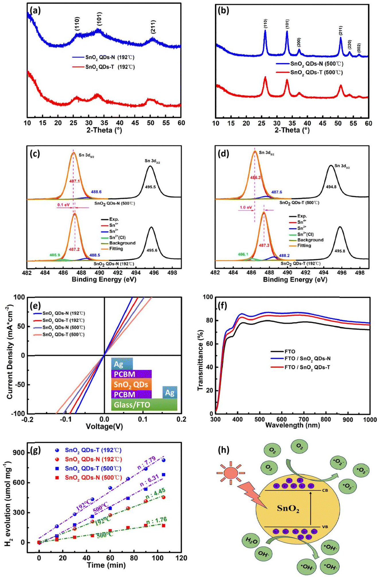 | ||
| Fig. 2 Interaction of SnO2 with the perovskite film. XRD patterns of SnO2 QDs annealed at (a) 192 °C and (b) 500 °C. Sn 3d XPS spectra from (c) SnO2 QDs-N and (d) SnO2 QDs-T samples. (e) J–V curves of the electron-only devices with an FTO/SnO2 QDs/Ag structure. (f) Transmission spectra of the SnO2 QDs-N and SnO2 QDs-T film on FTO substrates. (g) Photocatalytic H2 production rate and (h) Hydrogen evolution diagram of SnO2 QDs. | ||
The tin valence states were determined using X-ray photoelectron spectroscopy (XPS). At 192 °C, the Sn 3d core level exhibits a spin–orbit doublet with a splitting feature of 8.4 eV from Sn 3d5/2 (487.2 eV) and Sn 3d3/2 (495.6 eV) (Fig. 2c). From the asymmetric Sn 3d5/2 peak, there are three different valence states of ∼93.3% Sn4+, ∼3.5% Sn2+ and ∼3.2% Sn2+–Cl in the SnO2 QDs-N sample (Table S1, ESI†). The Cl 2p signal indicates an inadequate combustion reaction at 192 °C (Fig. S5a, ESI†). With doped thiourea, the corresponding characteristic peaks of Sn 3d shift up to 487.3 (Sn 3d5/2) and 495.8 (Sn 3d3/2) eV, respectively (Fig. 2d), along with ∼90.2% Sn4+, ∼6.1% Sn2+ and ∼3.7% Sn2+–Cl in the SnO2 QDs-T sample (Table S1, ESI†). At the binding energy (BE) of 400.0 eV, a small N 1s XPS signal could originate from the protonated-NH3+ or [(NH2)2N]+ of thiourea or its isomer on SnO2 QDs (Fig. S5b (ESI†) and Fig. 1d-III), which makes the corresponding spin–orbit splitting feature have an increase of 0.1 eV. Unfortunately, no sulfur peaks were found in the SnO2 QDs-T sample (Fig. S5b, ESI†), possibly because it was too little to be detected by XPS measurements. When the annealed temperature increases to 500 °C, the chlorine peak cannot be detected due to the sufficient combustion reaction. For the SnO2 QDs-N sample, there is minimal change for tin valence states (with ca. 3.8% increase of Sn4+ content and a ca. 0.6% decrease of Sn2+ content) with a 0.1 eV peak-shift towards low BE for Sn 3d peaks (Fig. 2c). However, the bigger peak-shift towards low BE with a 1.0 eV offset occurs in SnO2 QDs-T (Fig. 2d), possibly from the thorough combustion for the resulting deprotonation, along with a noticeable valence state change (with Sn4+ content increasing from ∼90.2 to 95.1% and Sn2+ content decreasing from ∼6.1 to 4.9%, Table S1, ESI†). It can be sure that decreasing Sn4+, along with increasing Sn2+, can increase the corresponding oxygen vacancy for the increased carrier density,22 which contributes to electron transfer. However, excessive oxygen vacancies also result in carrier recombination and interface instability among SnO2 QDs. Fortunately, the SnO2 QDs-N sample possessed a higher content of Sn4+ and a lower content of Sn2+ compared to the SnO2 QDs-T sample whether they were annealed at 192 or 500 °C, suggesting that the SnO2 QDs-N sample can achieve more stable photoelectric properties when it is used as ETL in PSCs.
The conductivity of SnO2 QDs films was analyzed via the current (J)–voltage (V) curves of electron-only devices (FTO/PCBM/SnO2 QDs (30 nm)/PCBM/Ag), as shown in Fig. 2e. The linear characteristics between J and V demonstrate the formation of ohmic contact between PCBM and SnO2 QDs. Since FTO glass, PCBM and silver electrodes were prepared under the same conditions, the bigger slope signifies that the corresponding SnO2 QDs film has better conductivity. With SnO2 QDs film annealed at 192 °C, the SnO2 QDs-N-based electron-only device achieves a larger conductivity of 4.05 × 10⁻³ S m−1, and it is bigger than that of the SnO2 QDs-T based one (2.90 × 10⁻³ S m−1), which is confirmed from the result that the square resistance of SnO2 QDs-N film (25.86 MΩ) is smaller than that of the SnO2 QDs-T film (36.13 MΩ) (Table S2, ESI†). Due to the coordination of S2− with Sn2+ on the surface of SnO2 QDs,26,41 the coverage of the outward –NH3+ or [(NH2)2N]+ group on SnO2 QDs lengthens the electron migration path among SnO2 QDs, thereby decreasing the corresponding conductivity of the devices. High-quality crystallization decreases the bulk defects, along with the decreased conductivity for the SnO2 QDs film.22 Moreover, the sufficient combustion of thiourea leaves some mesopores in the SnO2 QDs film (Fig. S6, ESI†), which is harmful to electron transfer. Therefore, the SnO2 QDs-T-based device had a smaller conductivity (2.03 × 10⁻³ S m−1) compared to the SnO2 QDs-N based device (2.86 × 10⁻³ S m−1) at 500 °C.
The transmission spectra are shown in Fig. 2f. With SnO2 QDs deposited on FTO substrates, the improved transmittance could originate from the filler of SnO2 QDs into the gullies on the surface of FTO (Fig. S6a-d, ESI†), indicating that SnO2 QDs can efficiently manage the UV-visible light to make much more transmitted photons, which thereby increases the absorption chance by the perovskite photoactive layer.31 Noted that the transmittance for SnO2 QDs-T/FTO is slightly lower than that for SnO2 QDs-N/FTO. Therefore, this SnO2 QDs-N filling improves the short-circuit current (Jsc). High- and low-temperature annealing has no obvious effect on the transmittance of the SnO2 QDs-N/FTO and SnO2 QDs-T/FTO (not shown here). According to Tauc plot (αhν)2vs. photon energy, a 3.79 eV Eg for the SnO2 QDs-N is bigger than that of SnO2 QDs-T (3.42 eV) (Fig. S7a, ESI†). This decreased Eg could result from the protonated-NH3+ or [(NH2)2N]+ coverage of SnO2 QDs, affecting the surface photocatalytic activity in the larger wavelength light absorption range. Urbach energy (Eu) was determined by the equation  (α denotes to the absorbance). SnO2 QDs-N has a smaller Eu value of 13 meV than that of SnO2 QDs-T (102 meV) (Fig. S7b, ESI†), indicating that SnO2 QDs-N has fewer structural defects for the improved electron transfer.46
The active catalytic sites on/in SnO2 QDs, relating to oxygen vacancies and affecting the interface stability of heterojunction, were characterized through the hydrogen evolution reaction from water splitting (Fig. 2g and h). Here, SnO2 QDs were deposited on fluorine-doped tin oxide (FTO) and placed in a glass reaction vessel with quantified deionized water. For the SnO2 QDs-N sample at 192 °C, its photocatalytic performance reaches 4.45 μmol g−1 min−1 hydrogen yield under simulated solar light without a 420 nm cut filter, then the hydrogen yield decreases to 1.76 μmol g−1 min−1 with SnO2 QDs-N annealed at 500 °C, which originates from the decrease of oxygen–vacancies in bulk as well as the terminal hydroxyl functional groups on the surface of SnO2 QDs. With thiourea treatment, the protonated-NH3+ or [(NH2)2N]+ coverage not only alters the bandgap of SnO2 QDs, thereby resulting in high visible-light absorption for the enhanced separation of the photo-induced carriers but also increases the active-sites, thereby resulting in the improved photocatalytic performance. Therefore, the SnO2 QDs-T sample achieved a better photocatalytic performance [7.39 and 6.31 μmol g−1 min−1 at 192 and 500 °C, respectively] than the SnO2 QDs-N sample.
Fig. S6 (ESI†) shows the SEM and AFM images of SnO2 QDs on FTO substrates. At 192 °C, the SnO2 QDs-N sample fills into the ravines at GBs along with a square average roughness (RMS) of ca. 3.39 nm, then it increases to 4.96 nm at 500 °C, which is less than that of the SnO2 QDs-T sample (ca. 4.77 nm at 192 °C and 6.73 nm at 500 °C), indicating that the small average-sized QDs can smoothen the surface of FTO,47,48 helping to reduce the leakage current for the better performance of PSC devices. Especially a lot of the raised burrs appear in the SnO2 QDs-T sample under a high annealed temperature (Fig. S6d, ESI†), which originates from the thorough combustion of guanidinium thiocyanate. Thus, these burrs make SnO2 QDs form a microporous structure to obtain the bigger RMS.
The PSC devices with a glass/FTO/SnO2 QDs/perovskite (500 nm)/spiro-OMeTAD (125 nm)/Au structure were fabricated, as shown in Fig. S8 (ESI†). Though the optimization of concentration (SnCl2·2H2O in water during the synthesis process) and spin-speed, we found that the concentration of 30 mg mL−1 and spin-speed of 3000 rad min−1 for SnO2 QDs preparation can achieve the optimal device efficiency (Fig. S9, ESI†).49 All J–V curves were obtained under standard sunlight (Fig. 3a–d), and the detailed statistical results (including the open-circuit voltage (Voc), Jsc, fill factor (FF), and PCE) exhibit good reproducibility (Fig. S10, ESI†). When SnO2 QDs ETLs were annealed from 192 to 500 °C, the SnO2 QDs-N-based devices achieved a weakened performance with a decreased PCE from 24.37 to 23.60%, Voc from 1.167 to 1.133 V, Jsc from 24.82 to 24.78 mA cm−2, FF from 84.13 to 84.06%, and hysteresis index (HI) from 0.57 to 0.38% in the reverse-scan mode, which is because SnO2 QDs at 500 °C had a poor electron extraction, despite obtaining better crystallization. Fortunately, the terminal hydroxyl functional groups on the SnO2 surface were removed under ozone treatment to make Pb2+ direct coordination with O2− or I− direct coordination with Sn2+, which can smoothen the interface barrier to suppress carrier accumulation for electron transfer at the interface between SnO2 and perovskite, obtaining the decreased HI for the corresponding device. For SnO2 QDs-T-based devices, the corresponding photovoltaic properties also exhibited a similar decreased trend when the annealed temperature of SnO2 QDs-T increased from 192 to 500 °C, along with a dropped PCE from 23.92 to 22.45%, Voc from 1.152 to 1.113 V, Jsc from 24.70 to 24.15 mA cm−2, FF from 84.07 to 83.53%, and HI from 2.13 to 1.69%. From the champion device of the two types of PSCs, the SnO2 QDs-N-based device obtained a higher PCE (25.55%) and smaller HI (0.26%) than the SnO2 QDs-T-based device (Fig. S11, ESI†), which could be attributed to the no coverage of the protonated-NH3+ or [(NH2)2N]+ on SnO2 QDs. Therefore, this deprotonated behavior made the corresponding device achieve a stable steady-state output efficiency of 25.27% (Fig. S12, ESI†), which closely matched the efficiencies obtained from the J–V scans (Fig. S11a, ESI†).
 | ||
| Fig. 3 Photovoltaic performance. The illuminated J−V characteristics of the PSCs based on (a) and (c) SnO2-N and (b) and (d) SnO2-T annealed at 192 and 500 °C. (e) IPCE of PSCs based on SnO2 annealed at 192 °C. (f) Raman spectra of thiourea mixed with PbI2 annealed at different temperatures. | ||
To explore the performance improvement of PSCs, water contact angle and incident photocurrent conversion efficiency (IPCE) characterizations were also performed. For the SnO2 QDs-N sample, the smaller contact angle means superior infiltration (Fig. S13, ESI†), leading to better contact with perovskite components to trigger heterogeneous nucleation over the perovskite precursor film for the high-quality perovskite. Thus, some relatively large-sized (ca. 800 nm) crystals on SnO2 QDs-N are twice as large as those on SnO2 QDs-T (Fig. S14, ESI†). Moreover, no bright crystals (indicating no PbI2 residual, confirmed by XRD pattern, Fig. S15, ESI†) exist in the SnO2 QDs-N-based perovskite films. The improved perovskite grains can enhance light absorption, along with the enhanced incident photocurrent conversion efficiency (IPCE, Fig. 3e). The integrated Jsc calculated from the IPCE curves is 24.39 mA cm−2 for the SnO2 QDs-N-based devices (matches well with the results from the J–V curve, and their difference is less than 1%), which is the bigger than that for the SnO2 QDs-T-based devices (23.67 mA cm−2). Therefore, the thiourea modified SnO2 QDs have an adverse impact on the performance of PSC devices with it as ETL.
Raman and Fourier transform infrared spectroscopy (FTIR) analyses were used to explore the interaction of thiourea with perovskite (Fig. 3f and 4a). To avoid the strong fluorescence characteristics of perovskite, thiourea was mixed with the raw material component of perovskite at a molar ratio of 1![[thin space (1/6-em)]](https://www.rsc.org/images/entities/char_2009.gif) :1. When the thiourea + PbI2 sample was annealed at 150 °C, two peaks appear at 106 and 197 cm−1, ascribing to the typical signatures of PbI2.50,51 With the annealed temperature increasing to 192 °C, two peaks shift to 109 and 214 cm−1, respectively. A new peak at 167 cm−1 is probably due to multi-phonon interactions between PbI2 and thiourea. Besides the intensity improvement of the above three peaks, another new peak appeared at 141 cm−1 when the annealed temperature increased to 250 °C. A first explanation for the appearance of new bands could be linked to a compression effect resulting from the ammonia penetration in the van der Waals spaces, which activates Raman vibrational modes situated at the low-frequency range of the spectrum. Another effect could result from the interaction between the unpaired electrons of sulphur/nitrogen atoms with PbI2.52
:1. When the thiourea + PbI2 sample was annealed at 150 °C, two peaks appear at 106 and 197 cm−1, ascribing to the typical signatures of PbI2.50,51 With the annealed temperature increasing to 192 °C, two peaks shift to 109 and 214 cm−1, respectively. A new peak at 167 cm−1 is probably due to multi-phonon interactions between PbI2 and thiourea. Besides the intensity improvement of the above three peaks, another new peak appeared at 141 cm−1 when the annealed temperature increased to 250 °C. A first explanation for the appearance of new bands could be linked to a compression effect resulting from the ammonia penetration in the van der Waals spaces, which activates Raman vibrational modes situated at the low-frequency range of the spectrum. Another effect could result from the interaction between the unpaired electrons of sulphur/nitrogen atoms with PbI2.52
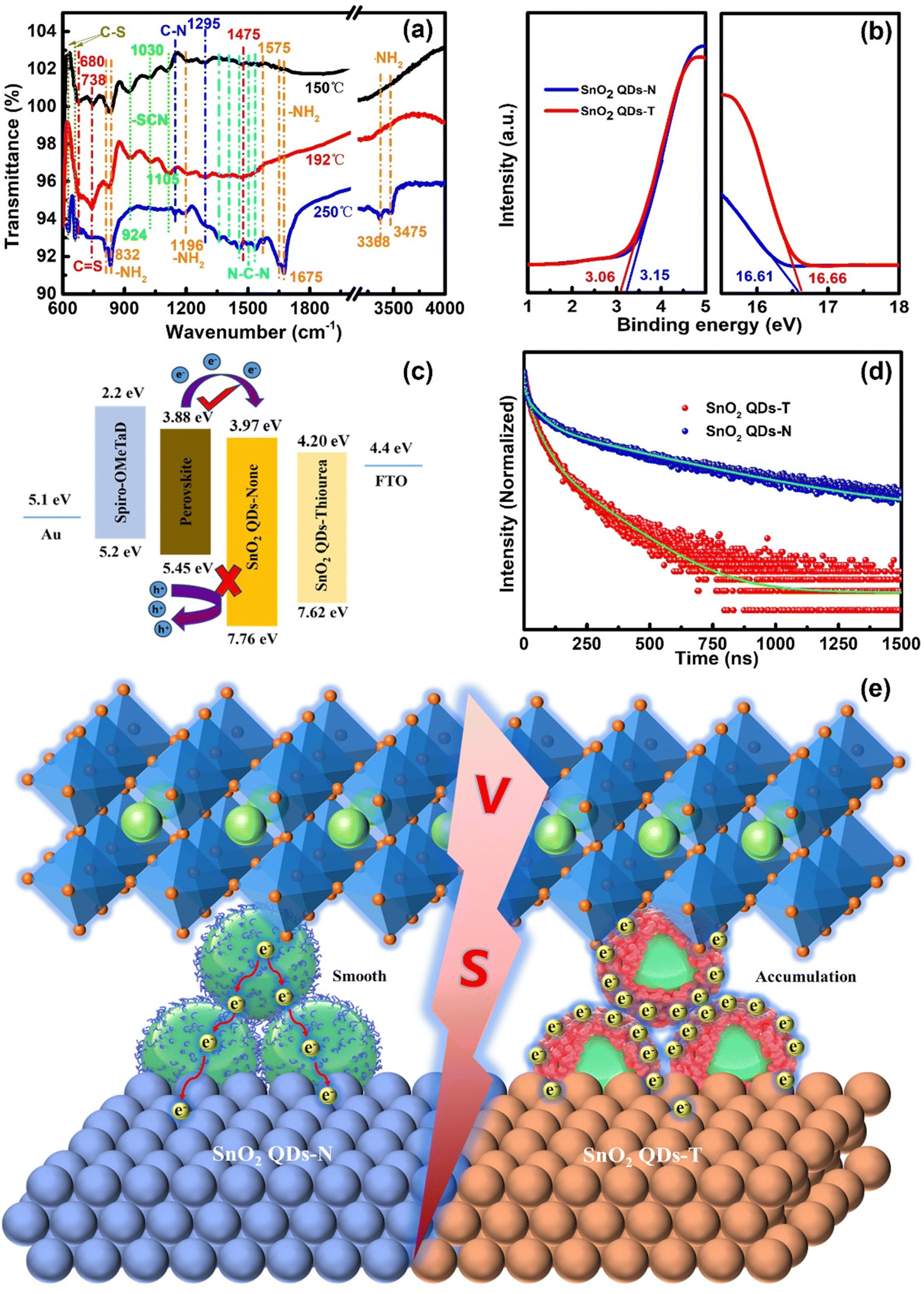 | ||
| Fig. 4 Carrier transport mechanism: (a) FTIR spectra of thiourea mixed with PbI2 annealed at different temperatures. (b) Secondary-electron cut-off and valence band region from the UPS of SnO2 QDs film. (c) Energy level diagram of PSCs. (d) Normalized TRPL of perovskite on SnO2 QDs. (e) Electro-migration diagram at the interface between perovskite and SnO2 QDs. | ||
From the FTIR results, it was also found that thiourea can completely react with PbI2 at 150 °C.44 The signals at 624 and 660 cm−1 correspond to the C–S stretching vibration (Fig. 4a). The C![[double bond, length as m-dash]](https://www.rsc.org/images/entities/char_e001.gif) S stretching vibrations at 680, 738 and 1475 cm−1 were not found.53 More double bond characteristics appear at 1356, 1408 (N–C–N symmetric stretching vibration), 1455 (N–C–N anti-symmetric stretching vibration), 1501 and 1538 cm−1, along with C–N stretching vibrations at 1144 and 1295 cm−1, indicating that thiourea processed the complex isomeric reaction via the coordination of the CS bond in thiourea with the Pb2+ in PbI2.54 Pb–S and Pb–I bonds are mainly electrovalent bonds. Unfortunately, the FTIR spectra did not show these bands associated with stretching and bending vibrations. Four peaks at 810 & 832 and 1575 & 1647 cm−1 are attributed to the N–H out-of-plane and in-plane deformation vibration, and those at 1196 and 1675 cm−1 are attributed to NH2-rock and N–H bending stretching vibrations,46 along with the asymmetric and symmetric stretching vibrations of NH2 at 3475 and 3368 cm−1. These results manifest that the isomerism and coupling reactions are quite complex. When the annealed temperature increased from 192 to 250 °C, the above two C–S bands and five N–C–N stretching vibrations, including five signals (related to NH2) at 1575, 1647, 1675, 3475 and 3368 cm−1, appear. Due to the delocalization of the lone pairs of electrons, the part of CN symmetric stretching vibration changes to –SCN, and then the three peaks at 924, 1025, and 1105 cm−1 disappear, along with the CS stretching vibration at 680, 738 and 1475 cm−1. However, the N–H out-of-plane deformation vibration at 832 cm−1 and the NH2-rock vibration at 1196 cm−1 are still present (Fig. 4a). These band-changes exhibit the rich dynamical formation and decomposition behavior of guanidinium thiocyanate, which could re-orientate or redistribute the organic cation groups.
S stretching vibrations at 680, 738 and 1475 cm−1 were not found.53 More double bond characteristics appear at 1356, 1408 (N–C–N symmetric stretching vibration), 1455 (N–C–N anti-symmetric stretching vibration), 1501 and 1538 cm−1, along with C–N stretching vibrations at 1144 and 1295 cm−1, indicating that thiourea processed the complex isomeric reaction via the coordination of the CS bond in thiourea with the Pb2+ in PbI2.54 Pb–S and Pb–I bonds are mainly electrovalent bonds. Unfortunately, the FTIR spectra did not show these bands associated with stretching and bending vibrations. Four peaks at 810 & 832 and 1575 & 1647 cm−1 are attributed to the N–H out-of-plane and in-plane deformation vibration, and those at 1196 and 1675 cm−1 are attributed to NH2-rock and N–H bending stretching vibrations,46 along with the asymmetric and symmetric stretching vibrations of NH2 at 3475 and 3368 cm−1. These results manifest that the isomerism and coupling reactions are quite complex. When the annealed temperature increased from 192 to 250 °C, the above two C–S bands and five N–C–N stretching vibrations, including five signals (related to NH2) at 1575, 1647, 1675, 3475 and 3368 cm−1, appear. Due to the delocalization of the lone pairs of electrons, the part of CN symmetric stretching vibration changes to –SCN, and then the three peaks at 924, 1025, and 1105 cm−1 disappear, along with the CS stretching vibration at 680, 738 and 1475 cm−1. However, the N–H out-of-plane deformation vibration at 832 cm−1 and the NH2-rock vibration at 1196 cm−1 are still present (Fig. 4a). These band-changes exhibit the rich dynamical formation and decomposition behavior of guanidinium thiocyanate, which could re-orientate or redistribute the organic cation groups.
The work function (WF) and valence band (VB) of SnO2 QD ETLs were determined by ultraviolet photoelectron spectroscopy (UPS, Fig. 4b). The cut-off binding energies (Ecut-off) were calculated as 16.61 and 16.66 eV, corresponding to the WFs of 4.61 and 4.56 eV for SnO2 QDs-N and SnO2 QDs-T, respectively. A 0.05 eV offset could originate from the surroundings of protonated-NH3+ or -[(NH2)2N]+ on the SnO2 QDs surface. From the VB characteristics of 3.15 and 3.06 eV, the ionization energies (IE) were estimated to be 7.76 and 7.62 eV for SnO2 QDs-N and SnO2 QDs-T, respectively (Fig. 4c). The lower IE can effectively block hole reverse migration,11 suppressing the unnecessary non-radiative recombination at this interface. Utilizing the direct bandgaps of 3.79 and 3.42 eV (Fig. S7a, ESI†), the corresponding electron affinities (EA) were estimated to be 3.97 and 4.20 eV, respectively. Thus, an energy level offset (ΔE) of 0.09 eV presents between SnO2 QD-N and perovskite, which is smaller than that between SnO2 QD-T and perovskite (0.32 eV), indicating that SnO2 QD-N as ETL can smoothen the interface barrier for electron transfer and extraction, avoiding charge accumulation at the interface for the reduced hysteresis of the PSC device.
The steady-state photoluminescence (PL) and time-resolved photoluminescence (TRPL) analyses were carried out to estimate carrier transfer between perovskite and SnO2 QDs. Compared to the SnO2 QDs-T-based perovskite, the SnO2 QDs-N-based perovskite exhibits an increased PL intensity at 788 nm (Fig. S16, ESI†), attributing to the high-quality perovskite film when the perovskite films were deposited on SnO2 QDs-N.33 TRPL spectra display a bi-exponential decay with a fast (τ1) and a slow (τ2) component (Fig. 4d). For the SnO2 QDs-N sample, τ1 and τ2 were 13.8 (13.2%) and 320.1 ns (86.8%), respectively (Table S3, ESI†). The τ1 increased to 24.6 ns (17.1%), while the τ2 decreased to 193.7 ns (82.9%) for the SnO2 QDs-T sample, which could be due to the quasi-core–shell structure of SnO2 QDs-T. Since the sulfur atoms in thiourea/its isomer were prone to coordination with Sn2+, the outward protonated-NH3+ or [(NH2)2N]+ groups, as shells, presented O2− in SnO2 not to crosslink directly with uncoordinated Pb2+ in the perovskite, not only increasing the electron-transport-length to decay electron transfer for the increasing τ1 but also prematurely recombined with the transferred electrons to decay electron extraction for the improved HI of PSC devices. Moreover, the poor infiltration cannot achieve the better-triggered effect for heterogeneous nucleation over the perovskite precursor film, and the formed poor perovskite film obtained the decreased τ2, which could weaken the performance of PSC devices with charge accumulation at the perovskite/SnO2 QDs interface (Fig. 4e).
Similarly, the results from the transient photoluminescence microscopy (TPLM, as a characterization tool for trap-states) further supported the above perspective. Here, a near-diffraction limited pulsed excitation laser (λex = 405 nm, 35 ps pulse) was used to generate a narrow initial exciton population and then focused on the bottom perovskite film at 31 ns to generate a near-diffraction-limited spot. As the delay time increased, the excitons began to diffuse, and the corresponding distribution width accordingly changed,51 from which the trap-state dynamics information related to GBs in the perovskite was extracted (Fig. 5a). At the diffraction limit spot (31 ns), the SnO2 QDs-N sample obtained the maximum photon number (15113), which was the higher than that (4235) from the SnO2 QDs-T sample (Fig. S17, ESI†). When the decay time was kept at 71 ns, the maximum photon number for the SnO2 QDs-N sample was 262, whereas the SnO2 QDs-T sample reduced to 151 counts at the shorter decay time of 52 ns (Fig. 5a and Fig. S17, ESI†),51 which indicates that the high-quality perovskite film on SnO2 QDs-N can achieve longer carrier lifetimes than that on SnO2 QDs-T. The exciton diffusion anisotropy is slightly higher along the y-axis than along the x-axis (Fig. S18, ESI†), which could be due to the influence of GBs in the perovskite.55,56
 | ||
| Fig. 5 Defects and stability of the PSCs based on SnO2 QDs-N and SnO2 QDs-T. (a) TPLM of perovskite films on SnO2 QDs-N from the FTO side. SCLC characteristics of (b) electron-only, the corresponding structure is shown in the inset. (c) EIS, (d) dark J–V curves and (e–g) long-term stability of the PSC devices. (h) X-ray response. There were 18 devices for each condition to carry out the aging process. | ||
Space charge-limited current (SCLC) measurements were used to investigate the electron-only devices with a structure of FTO/SnO2 QDs/perovskite (500 nm)/PCBM/Ag in depth. For the SnO2 QDs-N-based devices, the trap filling limit voltage (VTFL) is 0.09 V from the J–V curves (Fig. 5b), corresponding to the calculated electron trap state density (ntrap) of 2.16 × 1015 cm−3, which is smaller than that of the SnO2 QDs-T-based devices with a VTFL of 0.12 V as well as ntrap of 2.88 × 1015 cm−3. The electrochemical impedance spectroscopy (EIS) responses are shown in Fig. 5c. For the SnO2 QDs-N-based device, the charge transfer resistance (RTR) and recombination resistance (RREC) are 36.7 Ω and 3.25 × 10³ Ω, respectively. In contrast, RTR increases to 193.3 Ω, and RREC decreases to 3.94 × 10³ Ω for the SnO2 QDs-T-based device. The smaller RTR is beneficial to the extraction of charge, and the larger RREC can effectively inhibit charge recombination.57 These results indicate that SnO2 QDs-N can effectively suppress the defects at the perovskite/SnO2 QDs interface, thus greatly reducing the non-radiative recombination loss to smoothen electron transfer and extraction for the enhanced Jsc,58 which was confirmed by the lower leakage current density of the SnO2 QDs-N based PSCs compared that of the SnO2 QDs-T based device. (Fig. 5d)
The storage stability of unencapsulated devices was investigated in a dry and dark box (∼25% humidity, room temperature of ca. 25 °C). After 327 hours, the normalized PCE of the SnO2 QDs-T-based PSCs decayed to 90.0% of its initial value, whereas the SnO2 QDs-N-based PSCs decayed to the same efficiency over 1300 hours (Fig. 5e), and the storage stability was improved at a factor of ca. 4.0. Moreover, the thermal stability of T70 (PCE decay with 30%) increased from 140 hours for the SnO2 QDs-T-based PSCs to 372 hours for the SnO2 QDs-N-based PSCs, obtaining a factor of ca. 2.7 higher under annealing at 80 °C (Fig. 5f). Similarly, the normalized PCE of these devices exhibited a decay trend under white light illumination (ca 0.8 sun in ambient air, Fig. 5g), and decayed much faster than thermal (85 °C) only degradation. The photostability of T60 increased from 85 hours for SnO2 QDs-T-based PSCs to 286 hours for the SnO2 QDs-N-based PSCs with a factor of ∼4.8. These could originate from higher quality perovskite formation on SnO2 QDs-N ETLs than that on SnO2 QDs-T ETLs, which could suppress ion migration and prevent moisture (or oxygen) invasion into perovskite to achieve long-term storage, thermal and photothermal stability of the PSC devices.59
For SnO2 QDs-N, there was not only suitable for the photovoltaic field, but also played a powerful role in the X-ray detection. A thick perovskite layer (∼300 μm) was prepared on SnO2 QDs substrates to explore the current response from the X-ray detector using an FTO/SnO2 QDs/FA0.5FA0.5PbI3/Au structure. The time-dependent current curves of the devices at 1 V bias are shown in Fig. 5h. Both types of devices exhibit fast response speed and reproducible characteristics. In comparison, the SnO2 QDs-N-based device exhibits a diminished dark J (1.99 × 10⁻⁸ A cm−2) and enhances X-ray response J (2.14 × 10⁻⁷ A cm−2), along with 36 ms response time and 7.13 switch ratio, which is superior to those of the SnO2 QDs-T-based device (dark J 2.06 × 10⁻⁸ A cm−2, response J 1.09 × 10⁻⁷ A cm−2, 138 ms response time, and 2.25 switch ratio). This could be attributed to the rapid carrier migration among SnO2 QDs-N or between SnO2 QDs-N and high-quality perovskite crystal triggered by SnO2 QDs-N.
Conclusion
In summary, we have synthesized SnO2 QD ETLs by solution method to explore the surface protonation behavior of SnO2 QDs on the performance of PSCs. With no thiourea-treated SnO2 QDs, the prepared SnO2 QDs not only directly trigger heterogeneous nucleation over the perovskite precursor via the direct coordination of Pb2+ with O2− or I− with Sn2+ for the higher quality perovskite film, but also achieve the direct contact among SnO2 QDs, which can smoothen the interface barrier at the interface between SnO2 QDs and perovskite and among SnO2 QDs, facilitating rapid electron transfer for reduced non-radiative recombination. With thiourea doped into water solution, the surface protonation of SnO2 QDs exhibits strong electrostatic repulsion among SnO2 QDs due to the positive charge, which not only leads to electron recombination but also lengthens the electron migration path to decay electron transfer among SnO2 QDs. Furthermore, this surface protonation decreases the band gap, thereby resulting in an increased surface photocatalytic activity for the unstable interface. After thiourea was fully burned at high temperatures, the well-crystallized SnO2 achieved decreased intrinsic (bulk or surface) defects but weakened its n-type conductivity to harm electron migration and extraction compared to that at low-temperature annealing. Consequently, the SnO2 QDs-N-based PSC achieved an improved champion PCE of 25.55% and retained 95% of the initial PCE with 1000 h of storage in ambient air, far beyond the SnO2 QDs-T-based device. The corresponding X-ray detector also exhibits superior detection performance. The findings provide valuable insights into the wrapping behavior of quantum dots on non-radiative recombination and carrier transport at the interface, paving a pathway to develop stable and efficient PSCs for practical applications.Data availability
The data that support the findings of this study are available from the corresponding author on request. The data are not publicly available due to privacy or ethical restrictions.Conflicts of interest
The authors declare no conflict of interest.Acknowledgements
The manuscript was written through contributions from all authors. All authors have given approval to the final version of the manuscript. The work is supported by the Graduate Education Innovation Fund (CX2023272, CX2023277, CX2023279) of the Wuhan Institute of Technology.References
- Q. Fu, X. Tang, B. Huang, T. Hu, L. Tan, L. Chen and Y. Chen, Adv. Sci., 2018, 5, 1700387 CrossRef.
- L. Yan, J. Ma, P. Li, S. Zang, L. Han, Y. Zhang and Y. Song, Adv. Mater., 2022, 34, 2106822 CrossRef CAS PubMed.
- H. Zhou, Q. Chen, G. Li, S. Luo, T.-B. Song, H.-S. Duan, Z. Hong, J. You, Y. Liu and Y. Yang, Science, 2014, 345, 542–546 CrossRef CAS.
- C.-S. Jiang, M. Yang, Y. Zhou, B. To, S. U. Nanayakkara, J. M. Luther, W. Zhou, J. J. Berry, J. van de Lagemaat, N. P. Padture, K. Zhu and M. M. Al-Jassim, Nat. Commun., 2015, 6, 8397 CrossRef CAS.
- Z. Yu and L. Sun, Adv. Energy Mater., 2015, 5, 1500213 CrossRef.
- Z. Ren, K. Liu, H. Hu, X. Guo, Y. Gao, P. W. K. Fong, Q. Liang, H. Tang, J. Huang, H. Zhang, M. Qin, L. Cui, H. T. Chandran, D. Shen, M.-F. Lo, A. Ng, C. Surya, M. Shao, C.-S. Lee, X. Lu, F. Laquai, Y. Zhu and G. Li, Light: Sci. Appl., 2021, 10, 239 CrossRef CAS.
- Q. Lou, Y. Han, C. Liu, K. Zheng, J. Zhang, X. Chen, Q. Du, C. Chen and Z. Ge, Adv. Energy Mater., 2021, 11, 2101416 CrossRef CAS.
- D. H. Kim, C. P. Muzzillo, J. Tong, A. F. Palmstrom, B. W. Larson, C. Choi, S. P. Harvey, S. Glynn, J. B. Whitaker, F. Zhang, Z. Li, H. Lu, M. F. A. M. van Hest, J. J. Berry, L. M. Mansfield, Y. Huang, Y. Yan and K. Zhu, Joule, 2019, 3, 1734–1745 CrossRef CAS.
- G. E. Eperon, T. Leijtens, K. A. Bush, R. Prasanna, T. Green, J. T.-W. Wang, D. P. McMeekin, G. Volonakis, R. L. Milot, R. May, A. Palmstrom, D. J. Slotcavage, R. A. Belisle, J. B. Patel, E. S. Parrott, R. J. Sutton, W. Ma, F. Moghadam, B. Conings, A. Babayigit, H.-G. Boyen, S. Bent, F. Giustino, L. M. Herz, M. B. Johnston, M. D. McGehee and H. J. Snaith, Science, 2016, 354, 861–865 CrossRef CAS PubMed.
- R. Prasanna, A. Gold-Parker, T. Leijtens, B. Conings, A. Babayigit, H.-G. Boyen, M. F. Toney and M. D. McGehee, J. Am. Chem. Soc., 2017, 139, 11117–11124 CrossRef CAS PubMed.
- C. Shi, J. Li, S. Xiao, Z. Wang, W. Xiang, R. Wu, Y. Liu, Y. Zhou, W. Ke, G. Fang and P. Qin, J. Energy Chem., 2024, 93, 243–252 CrossRef CAS.
- NREL., 2024.
- L. Yang, J. Feng, Z. Liu, Y. Duan, S. Zhan, S. Yang, K. He, Y. Li, Y. Zhou, N. Yuan, J. Ding and S. Liu, Adv. Mater., 2022, 34, 2201681 CrossRef CAS PubMed.
- Z. Xiong, X. Chen, B. Zhang, G. O. Odunmbaku, Z. Ou, B. Guo, K. Yang, Z. Kan, S. Lu, S. Chen, N. A. N. Ouedraogo, Y. Cho, C. Yang, J. Chen and K. Sun, Adv. Mater., 2022, 34, 2106118 CrossRef CAS PubMed.
- C. Altinkaya, E. Aydin, E. Ugur, F. H. Isikgor, A. S. Subbiah, M. De Bastiani, J. Liu, A. Babayigit, T. G. Allen, F. Laquai, A. Yildiz and S. De Wolf, Adv. Mater., 2021, 33, 2005504 CrossRef CAS.
- Y. Dong, W. Shen, W. Dong, C. Bai, J. Zhao, Y. Zhou, F. Huang, C. Yi-Bing and J. Zhong, Adv. Energy Mater., 2022, 12, 2200417 CrossRef CAS.
- H. Min, D. Y. Lee, J. Kim, G. Kim, K. S. Lee, J. Kim, M. J. Paik, Y. K. Kim, K. S. Kim, M. G. Kim, T. J. Shin and S. I. Seok, Nature, 2021, 598, 444–450 CrossRef CAS.
- J. Park, J. Kim, H.-S. Yun, M. J. Paik, E. Noh, H. J. Mun, M. G. Kim, T. J. Shin and S. I. Seok, Nature, 2023, 616, 724–730 CrossRef CAS PubMed.
- J. J. Yoo, G. Seo, M. R. Chua, T. G. Park, Y. Lu, F. Rotermund, Y.-K. Kim, C. S. Moon, N. J. Jeon, J.-P. Correa-Baena, V. Bulovic, S. S. Shin, M. G. Bawendi and J. Seo, Nature, 2021, 590, 587 CrossRef CAS PubMed.
- P. Qin, T. Wu, Z. Wang, X. Zheng, X. Yu, G. Fang and G. Li, Sol. RRL, 2019, 3, 1900134 CrossRef CAS.
- J. M. Ball and A. Petrozza, Nat. Energy, 2016, 1, 1–13 Search PubMed.
- X. Li, Z. Shi, F. Behrouznejad, M. Hatamvand, X. Zhang, Y. Wang, F. Liu, H. Wang, K. Liu, H. Dong, F. Mudasar, J. Wang, A. Yu and Y. Zhan, J. Energy Chem., 2022, 67, 1–7 CrossRef CAS.
- R. Wu, L. Xiao, Z. Wang, C. Shi, S. Xiao, W. Xiang, Z. Qin, X. Chen, G. Fang and P. Qin, J. Mater. Chem. A, 2023, 11, 22409–22418 RSC.
- Z. Wang, T. Wu, L. Xiao, P. Qin, X. Yu, L. Ma, L. Xiong, H. Li, X. Chen, Z. Wang, T. Wu, L. Xiao, P. Qin, X. Yu, L. Ma, L. Xiong, H. Li and X. Chen, J. Power Sources, 2021, 488, 229451 CrossRef CAS.
- J. P. C. Baena, L. Steier, W. Tress, M. Saliba, S. Neutzner, T. Matsui, F. Giordano, T. J. Jacobsson, A. R. S. Kandada, S. M. Zakeeruddin, A. Petrozza, A. Abate, M. K. Nazeeruddin, M. Graetzel and A. Hagfeldt, Energy Environ. Sci., 2015, 8, 2928–2934 RSC.
- X. Zhou, R. Kong, R. Liu, Y. Liu, M. Liang, Z. Shen, F. Li, M. Jin, D. Yang, S. Wang, H. Li, R. Cao and C. Chen, J. Mater. Chem. C, 2023, 11, 13774–13781 RSC.
- Y. Zhang, D. Zherebetskyy, N. D. Bronstein, S. Barja, L. Lichtenstein, D. Schuppisser, L.-W. Wang, A. P. Alivisatos and M. Sameron, Nano Lett., 2015, 15, 3249–3253 CrossRef CAS.
- G. Yang, C. Chen, F. Yao, Z. Chen, Q. Zhang, X. Zheng, J. Ma, H. Lei, P. Qin, L. Xiong, W. Ke, G. Li, Y. Yan and G. Fang, Adv. Mater., 2018, 30, 1706023 CrossRef.
- L. Zhang, C. Fu, S. Wang, M. Wang, R. Wang, S. Xiang, Z. Wang, J. Liu, H. Ma, Y. Wang, Y. Yan, M. Chen, L. Shi, Q. Dong, J. Bian and Y. Shi, Adv. Funct. Mater., 2023, 33, 2213961 CrossRef CAS.
- Q. Liu, M.-C. Qin, W.-J. Ke, X.-L. Zheng, Z. Chen, P.-L. Qin, L.-B. Xiong, H.-W. Lei, J.-W. Wan, J. Wen, G. Yang, J.-J. Ma, Z.-Y. Zhang and G.-J. Fang, Adv. Funct. Mater., 2016, 26, 6069–6075 CrossRef CAS.
- L. Xiong, M. Qin, C. Chen, J. Wen, G. Yang, Y. Guo, J. Ma, Q. Zhang, P. Qin, S. Li and G. Fang, Adv. Funct. Mater., 2018, 28, 1706276 CrossRef.
- K. Deng, Q. Chen and L. Li, Adv. Funct. Mater., 2020, 30, 2004209 CrossRef CAS.
- J. Kim, J. Park, Y.-H. Kim and W. Jo, Small, 2022, 18, 44 Search PubMed.
- E. H. Jung, B. Chen, K. Bertens, M. Vafaie, S. Teale, A. Proppe, Y. Hou, T. Zhu, C. Zheng and E. H. Sargent, ACS Energy Lett., 2020, 5, 2796–2801 CrossRef CAS.
- H.-S. Yun, Y.-H. Seo, C.-E. Seo, H. S. Kim, S. B. Yoo, B. J. Kang, N. J. Jeon and E. H. Jung, Adv. Energy Mater., 2024, 14, 2400791 CrossRef CAS.
- Y. Gao, M. Yan, C. Cheng, H. Zhong, B.-H. Zhao, C. Liu, Y. Wu and B. Zhang, J. Am. Chem. Soc., 2023, 146, 714–722 CrossRef PubMed.
- A. Bhattacharjee and M. Ahmaruzzaman, J. Colloid Interface Sci., 2015, 448, 130–139 CrossRef CAS PubMed.
- C. Sun, J. Yang, M. Xu, Y. Cui, W. Ren, J. Zhang, H. Zhao and B. Liang, Chem. Eng. J., 2022, 427, 131564 CrossRef CAS.
- C. Burda, X. Chen, R. Narayanan and M. A. El-Sayed, Chem. Rev., 2005, 105, 1025–1102 CrossRef CAS PubMed.
- L. Wang, R. Li, W. Chen, H. Wang and K. Chen, Acta Chim. Sin., 2009, 67, 838–842 CAS.
- X. Lu, H. Wang, Z. Wang, Y. Jiang, D. Cao and G. Yang, J. Alloys Compd., 2016, 680, 109–115 CrossRef CAS.
- T. Niu, F. Zhen, Y.-M. Xie, T. Yang, Q. Yao, J. Lu, K. Zhao and H.-L. Yip, ACS Appl. Mater. Interfaces, 2022, 14, 52838–52848 CrossRef CAS.
- C. Fei, B. Li, R. Zhang, H. Fu, J. Tian and G. Cao, Adv. Energy Mater., 2017, 7, 1602017 CrossRef.
- Z. D. Wang, M. Yoshida and B. George, Comput. Theor. Chem., 2013, 1017, 91–98 CrossRef CAS.
- P. P. Patel, P. J. Hanumantha, O. I. Velikokhatnyi, M. K. Datta, B. Gattu, J. A. Poston, A. Manivannan and P. N. Kumta, Mater. Sci. Eng., B, 2016, 208, 1–14 CrossRef CAS.
- A. Tricoli, M. Graf and S. E. Pratsinis, Adv. Funct. Mater., 2008, 18, 1969–1976 CrossRef CAS.
- Z. Xu, Y. Jiang, Z. Li, C. Chen, X. Kong, Y. Chen, G. Zhou, J.-M. Liu, K. Kempa and J. Gao, ACS Appl. Energy Mater., 2021, 4, 1887–1893 CrossRef CAS.
- C.-X. Zhao, J.-N. Liu, B.-Q. Li, D. Ren, X. Chen, J. Yu and Q. Zhang, Adv. Funct. Mater., 2020, 30, 2004209 CrossRef.
- J. Zhou, M. Lyu, J. Zhu, G. Li, Y. Li, S. Jin, J. Song, H. Niu, J. Xu and R. Zhou, ACS Appl. Energy Mater., 2022, 5, 3052–3063 CrossRef CAS.
- Z. Wang, C. Shi, Z. Wang, L. Xiao, T. Wu, X. Yu, L. Ma, X. Chen, J. Zhang, H. Lei and P. Qin, Chem. Eng. J., 2022, 441, 136118 CrossRef CAS.
- T. Meier, T. P. Gujar, A. Schoenleber, S. Olthof, K. Meerholz, S. van Smaalen, F. Panzer, M. Thelakkat and A. Koehler, J. Mater. Chem. C, 2018, 6, 7512–7519 RSC.
- N. Preda, L. Mihut, M. Baibarac, I. Baltog, R. Ramer, J. Pandele, C. Andronescu and V. Fruth, J. Mater. Sci.: Mater. Electron., 2009, 20, 465–470 CrossRef CAS.
- R. G. Kumari, V. Ramakrishnan, M. L. Carolin, J. Kumar, A. Sarua and M. Kuball, Spectrochim. Acta, Part A, 2009, 73, 263–267 CrossRef.
- A. K. Surca, A. Rauter, M. Rodosek, L. S. Perse, M. Kozeljj and B. Orel, Prog. Org. Coat., 2017, 103, 1–14 CrossRef CAS.
- J. Luo, L. Yang, Z. Tan, W. Xie, Q. Sun, J. Li, P. Du, Q. Xiao, L. Wang, X. Zhao, G. Niu, L. Gao, S. Jin and J. Tang, Adv. Mater., 2021, 33, 2101903 CrossRef CAS PubMed.
- Z. Ni, S. Xu, H. Jiao, H. Gu, C. Fei and J. Huang, Sci. Adv., 2022, 8(36), eabq8345 CrossRef CAS PubMed.
- Z. Zhu, J. Shang, G. Tang, Z. Wang, X. Cui, J. Jin, Y. Zhou, X. Zhang, D. Zhang, X. Liu and Q. Tai, Chem. Eng. J., 2023, 454, 140163 CrossRef CAS.
- C. Shi, S. Xiao, Z. Wang, W. Xiang, R. Wu, X. Yu, L. Ma, Z. Qin, L. Xiong, Q. Liu, X. Jiang, G. Fang and P. Qin, Sol. RRL, 2023, 7, 2300461 CrossRef CAS.
- E. Wang, P. Chen, X. Yin, Y. Wu and W. Que, Sol. RRL, 2019, 3, 1900041 CrossRef.
Footnotes |
| † Electronic supplementary information (ESI) available. See DOI: https://doi.org/10.1039/d4ee03193h |
| ‡ These authors contributed equally to this article. |
| This journal is © The Royal Society of Chemistry 2025 |