Controlled Au-coated PDMS microwell array for surface-enhanced DNA biochips†
Yeongseok
Jang
ab and
Jonghyun
Oh
 *c
*c
aDepartment of Mechanical Design Engineering, Jeonbuk National University, Jeonju-si 54896, Jeollabuk-do, Republic of Korea
bDivision of Engineering in Medicine, Department of Medicine, Brigham and Women's Hospital, Harvard Medical School, Cambridge, MA, 02139 USA
cDepartment of Nano-Bio Mechanical System Engineering, Jeonbuk National University, Jeonju-si 54896, Jeollabuk-do, Republic of Korea. E-mail: jonghyuno@jbnu.ac.kr; Tel: +82 6327 04572 Tel: +82 6327 02451
First published on 27th November 2024
Abstract
Microwell technology is crucial in biological applications due to its ability to handle small sample sizes and perform numerous assays efficiently. This study aimed to develop a novel technique for microwell fabrication using pressure-assisted steam technology, offering lower cost, simplicity, and high reproducibility. Mechanical properties of microwell surfaces were successfully controlled and characterized, making them suitable for DNA capture. The application of gold coating generated an electric field within designed microwells, facilitating stable DNA detection. These microwells exhibited effective DNA sensing capabilities, validated using fluorescently stained lambda DNA at various concentrations (86, 8.6, and 0.86 ng μL−1). In particular, the 2.8 mm microwell showed a greater change in fluorescence intensity depending on DNA concentration than other microwells. At a concentration of 0.86 ng μL−1, to assess producibility using relative standard deviation (RSD) values as a DNA sensor, they were measured as 5.29, 2.76, and 1.85% for 1, 1.7, and 2.8 mm microwells, respectively. These results indicated that our proposed microwell exhibited efficient performance and good reproducibility. We believe that the developed method could be potentially used for high-throughput analysis as a biosensor for DNA applications.
Introduction
Microwell technology has been developed for numerous applications of biological purposes. The utilization of microwells in biological applications offers several advantages, including the ability to work with small sample sizes, which may facilitate a higher number of assay runs. Additionally, parallelization of microwell arrays can enhance overall analysis speed and the presence of specific structures such as topological recesses can provide added benefits.1 Since 2000, several approaches of microwell fabrication have been reported to ensure uniformity of microwells.2 While photolithography offers high precision in patterning, it is often limited by the need for expensive equipment such as UV lithography systems and cleanroom facilities.3–8 Additionally, photolithography is typically restricted to the fabrication of 2D structures with multiple complex steps, making it difficult to use it in large-scale applications. Another existing method is soft-lithographic technology, which often utilizes polydimethylsiloxane (PDMS)-based materials.9–13 Although it enables relatively simple production of 3D structures, it still faces challenges in terms of reproducibility. For example, the use of molds for repeated production can result in wear and degradation over time, which affects the consistency of microwell sizes. To produce microwells of various shapes and sizes by a simple method, 3D printing technology and laser engraving have been introduced.14–19 However, these methods have disadvantages such as low precision, limited reproducibility, and time-consuming processes.On the other hand, array-based DNA nanotechnology has been applied in various fields, including medical diagnosis, biowarfare agent detection, cell biology, and forensic analysis.20,21 In 2004, an electroplated microwell array chip was fabricated. It demonstrated the feasibility of using an isolation mechanism for oligonucleotide DNA synthesis.22 In 2006, to achieve high analyte concentration from highly diluted samples, a patterned DNA microarray with a hydrophobic fluorocarbon polymer demonstrated the effectiveness of using a microconcentration process for improving DNA detection sensitivity.4 In 2009, a microwell cell culturing chip for PCR amplification and mutation analysis was developed, where cells were lysed and subjected to PCR directly in wells.23 In 2010, a microwell for DNA damage analysis was fabricated using agarose and Su-8 stamp produced by a photolithography method.24 In 2012, a photoelectrochemical DNA biosensor was investigated for rapid and high throughput performance. However, due to the lack of appropriate platforms, the potential of high throughput has not been demonstrated.25 In 2015, a microwell chip fabricated by multilayer soft lithography was introduced for DNA amplification of single cancer cells.26 In 2016, an automated microwell system exhibited a high-quality large-scale single cell RNA sequencing performance.27 In 2020, femtoliter-sized microwells with magnetic beads were created to detect multiplex nucleic acids without needing any target amplification. This system demonstrated the ability to detect nucleic acid targets in microwells down to femtomolar (fM) concentrations.28 In 2020, a digital PCR sensor composed of a PDMS and polymethyl methacrylate (PMMA) microwell array was applied in a plasmonic heating system.29 In 2021, microarray patterns produced based on the soft lithography technology were developed to perform multi-step, multi-reagent assays. This microfluidic array device has advantages of small volume sample consumption and cost effectiveness.30 Shen et al. have reported a rapid nucleic acid concentration determination system based on a white laser light source and analyzed fluorescence intensity with different DNA concentrations.31
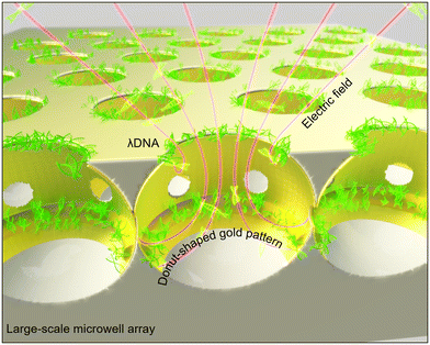
Methods developed so far for DNA application using microwells require the complex fabrication processes mentioned above. Given the disadvantages and limitations of conventional microwell fabrication methods, there is a need for a new strategy. Therefore, in this study, we present a novel technique for fabricating a microwell array using pressure-assisted steam technology. This pressure-assisted steam technology overcomes the limitations of previous methods by offering a simpler, scalable, and cost-effective approach for fabricating PDMS microwells. Our method does not require multiple complex steps. It enables the fabrication of microwells with varying sizes in a single process, which is not easily achievable with traditional methods. Additionally, controllable DNA capture can be achieved by the mechanical property of fabricated microwells' surfaces. The mechanical properties of fabricated microwells' surfaces were measured and characterized. A 300 nm gold layer on the microwells was coated using the E-beam process for application of electrical properties to the gold coated surface. The donut-shaped gold pattern generated an electric field inside the designed microwells, which facilitated stable DNA capture. DNA sensing performance was assessed using fluorescently stained lambda DNA with different concentrations to verify its feasibility for applications related to DNA detection (Fig. 1). Our proposed microwells present a useful and effective tool for DNA sensing as a biosensor. It is anticipated to be applicable to DNA sequencing, hybridization, and cell analysis.
Materials and methods
Fabrication of PDMS microwells
Silicone elastomer base at 4, 6, and 8 g was respectively mixed with a curing agent at a ratio of 10![[thin space (1/6-em)]](https://www.rsc.org/images/entities/char_2009.gif) :
:![[thin space (1/6-em)]](https://www.rsc.org/images/entities/char_2009.gif) 1 (Sylgard 184 silicone elastomer kit; Dow Corning, Midland, MI, USA). Mixed PDMS precursors were poured into 80 mm glass Petri dishes placed in a vacuum desiccator (DURAN Group GmbH, Mainz, Germany) to degas PDMS precursors for 5 minutes.
1 (Sylgard 184 silicone elastomer kit; Dow Corning, Midland, MI, USA). Mixed PDMS precursors were poured into 80 mm glass Petri dishes placed in a vacuum desiccator (DURAN Group GmbH, Mainz, Germany) to degas PDMS precursors for 5 minutes.
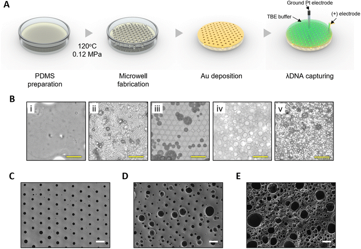
To prepare PDMS microwells, degassed PDMS precursors of silicone elastomer base at 4, 6, and 8 g were treated in a 0.12 MPa chamber (JSAT-85, JS Research Inc., Gongju, South Korea). Pressure-based steam technology operates at a pressure environment higher than atmospheric pressure using a sealed chamber and a heating mechanism. Upon heating, the water inside the chamber reached its boiling point at atmospheric pressure, generating water vapor. The chamber containing the vapor was then sealed and the pressure increased to 0.12 MPa at 120 °C. Microwells were fabricated in an environment where these temperature and pressure changed. In the first stage, the temperature was increased to 120 °C for 15 minutes, which created air bubbles inside the PDMS and caused them to travel upward. In the second stage, when the temperature of the chamber was stable at 120 °C, smaller bubbles in the PDMS mixture merged into one bubble, while the PDMS surface was simultaneously pressed by the pressure environment. Treatment time was 4, 10, or 12 minutes for 4, 6, or 8 g, respectively. Bubbles were aligned below the PDMS surface. In the last stage, pressure and temperature were lowered for 30 minutes, resulting in bursting and curing of aligned bubbles.
Characterization of PDMS microwells
Top, bottom, and cross-sections of PDMS microwells were visualized using a field-emission scanning electron microscope (FE-SEM) (SUPRA 40VP, Carl Zeiss Microscopy GmbH, Jena, Germany). Images were processed with ImageJ software (National Institutes of Health, MD, USA). The thickness of whole PDMS microwells, pore size, diameter, and height of a single microwell were investigated and quantitatively analyzed.Mechanical properties of three PDMS microwells were measured with an atomic force microscope (AFM) (XE-100, Park Systems Corp., Suwon, South Korea). Surface morphology was analyzed at a scan rate of 0.3 Hz in a tapping mode with the NCHR tip. The roughness was obtained for the scanned area of 40 × 40 μm2. The force–displacement (F/D) curve in the contact mode was recorded. Young's modulus was calculated from this curve using the Hertz model. The average value of Young's modulus was determined from measurements taken at five different points. All data were analyzed using the XEI software.
Gold coating of PDMS microwells
To allow for electrical properties, a 300 nm-thick Au layer was deposited on PDMS microwells using the E-beam process. Morphological and elemental analyses of Au-coated PDMS microwells were conducted using an FE-SEM with energy-dispersive X-ray spectroscopy (EDS) (ULTIM MAX 100, Oxford Instruments, Abingdon, United Kingdom). Accelerating voltages of 2 kV and 10 kV were used for image and EDS analysis, respectively. The line profile of Au element on the mapping images was obtained by analyzing the spectra collected.DNA detection and observation
To prepare DNA, lambda DNA (concentration of 0.3 μg μL−1) (SD0011, Thermo Scientific, Waltham, MA, USA) at a volume of 100 μl was stained with 7.5 μl of YOYO-1 dye (Y3601, Invitrogen, Carlsbad, CA, USA) and incubated in an oven at 55 °C for 2 hours. To eliminate the remaining dye, 100 μL of tris-borate-EDTA (TBE) buffer solution (T7527, Sigma-Aldrich, St. Louis, MO, USA) was added to the incubated mixture for washing, followed by centrifugation at 12![[thin space (1/6-em)]](https://www.rsc.org/images/entities/char_2009.gif) 000g for 2 minutes. This washing process was repeated three times. The washed DNA solution was then filtered using a 0.2 μm syringe filter. Finally, the filtered DNA solution was diluted to concentrations of 86, 8.6, and 0.86 ng μL−1 in TBE buffer.
000g for 2 minutes. This washing process was repeated three times. The washed DNA solution was then filtered using a 0.2 μm syringe filter. Finally, the filtered DNA solution was diluted to concentrations of 86, 8.6, and 0.86 ng μL−1 in TBE buffer.
To detect DNA, a PDMS mold with an 8 mm diameter hole was placed on the Au-coated PDMS microwells. Then 40 μL of stained lambda DNA solution was poured into the PDMS mold. A wire-type Pt electrode (99.95%, Taewon Scientific Co. Ltd., Seoul, South Korea) with a diameter of 1 mm was positioned 1 mm above the floor of Au-coated PDMS microwells and connected to the ground. Silver epoxy was used to attach a positive (+) electrode to the surface of Au-coated PDMS microwells (Fig. 2A).
Electrical stimulation time for constant DNA detection was optimized by applying 0 and +2 V to Au-coated PDMS microwells using a power supply (GPD-4303S, Good Will Instrument Co. Ltd., New Taipei, Taiwan) for 0, 10, 30, and 60 seconds. The DNA sensing performance of the PDMS microwells was evaluated with different stained DNA concentrations of 86, 8.6, and 0.86 ng μL−1. Following the electrophoresis test, electrodes were removed and surfaces of Au-coated PDMS microwells were washed three times with deionized (DI) water using vigorous pipetting to remove any unattached DNA. Subsequently, the PDMS mold was removed.
Fluorescence images with fluorescently-stained lambda DNAs were obtained using a confocal laser scanning microscope (LSM 510 META, Carl Zeiss, Jena, Germany). The fluorescence intensity of each microwell with a thickness of 1.0 mm, 1.7 mm, or 2.7 mm was quantitatively analyzed using ImageJ software and compared. The intensity for quantification of DNA attached to the inside of microwell according to lambda DNA concentration (86, 8.6, and 0.86 ng μL−1) was examined. Five samples were used for each analysis and 20 single microwells were measured for each sample at different thickness of microwells and concentration of lambda DNA.
Statistical analysis
Data are presented as mean ± standard deviation (SD). They were results of five independent experiments for each sample. Statistical significance was determined with one-way analysis of variance (ANOVA) with Tukey's multiple comparison tests. A p-value less than 0.05 was considered as significant.The limit of detection (LOD) was determined using the following formula: LOD = 3Sb/S (Sb: the standard deviation of the blank signal, S: the slope of the concentration peak intensity of the calibration curve).32 All experiments for LOD data were performed five times using 20 single microwells for each independent analysis.
Results and discussion
Fabrication and characterization of the PDMS microwell array
PDMS microwells were generated by a pressure-based steam technology including three stages (Fig. 2). Bubbles generated from mixing of the PDMS base and curing agent were placed inside the PDMS mixture. In the first stage, as the temperature increased to 120 °C for 15 minutes, very small, invisible bubbles in the PDMS mixture lifted from the bottom (Fig. 2(B, i)). In the second stage, before the PDMS mixture was fully cured, bubbles merged and grew larger as they approached the surface. Under a pressure of 0.12 MPa at 120 °C, bubbles located just below the surface, where further rise was restricted, were aligned below the PDMS surface for an appropriate treatment time depending on the membrane thickness (Fig. 2(B, ii)). Different treatment times of 4, 10, and 12 minutes were used to fabricate microwells using 4, 6, and 8 g of elastomer base, respectively. As the amount of elastomer base increased, the height at which bubbles lifted also increased, thereby increasing the processing time. Finally, bubbles were densely packed together, forming a uniform array structure. In the last stage, upon pressure release and a temperature decrease for 30 minutes, bubbles on the surface burst and cured completely to form microwells (Fig. 2(B, iii)).To further understand the fabrication process for microwells, the PDMS surface (8 g of elastomer base) was observed after treatment for a longer time (15 and 20 minutes) than the microwell fabrication time. As the treatment time increased, the irregularity in microwell size also increased (Fig. 2(B, iv and v)). Fig. 2C–E show representative FE-SEM images in Fig. 2B(iii–v), respectively. The increase of irregularity over time could be attributed to continuous merging and division of microwells within the PDMS mixture prior to curing under a pressure of 0.12 MPa. Therefore, treatment time plays a crucial role in achieving a consistent microwell array. On the other hand, at temperatures below 100 °C and during the same processing time, the pressure did not reach 0.12 MPa, which was presumed to be insufficient to provide the necessary pressure for microwells to align (Fig. S1†). In addition, microwells were not formed at any temperatures under atmospheric pressure. This could be attributed to the fact that the bubbles rising within the PDMS mixture escaped once they reached the surface, as bubbles were affected by atmospheric pressure.
The thickness of each microwell membrane fabricated with 4, 6, or 8 g of elastomer base was 1, 1.7, or 2.8 mm, respectively (Fig. S2†). The membrane size was 4 × 4 cm, enabling the production of large-scale microwells (Fig. S3†).
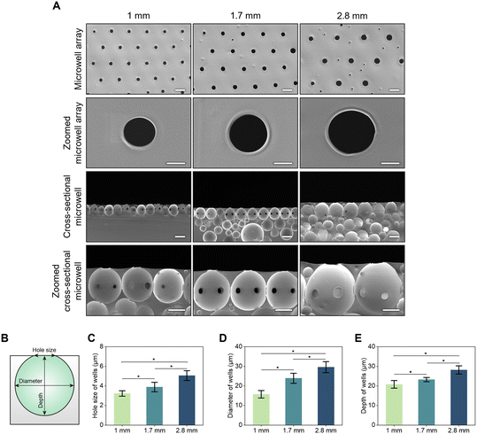
Fig. 3A shows the surface and cross-sectional images of fabricated microwells according to membrane thickness. As the membrane thickness increased, the production rate of microwells per unit area decreased. During the microwell fabrication process, as the pressure decreased, a hole was produced on the surface of the membrane, which became the entrance to the microwell. The smallest microwell pore size was observed in a 1 mm thick membrane. As seen in cross-sectional images of microwells, increasing the thickness of the membrane led to an increase in the number of bubbles beneath microwells on the surface. The largest microwell appeared in a 2.8 mm thick membrane. All microwells on the top layer were connected to each other at all conditions.
Fig. 3B shows a schematic of a single microwell. To quantitatively analyze the dependency of pore size, diameter, and depth of the microwell according to membrane thickness, the size of a single microwell was measured (Fig. 3C). Pore sizes of microwells were 3.23 ± 0.28 μm, 3.88 ± 0.48 μm, and 5.05 ± 0.51 μm for membrane thicknesses of 1, 1.7 and 2.8 mm, respectively. As confirmed in the FE-SEM image, the diameter of the microwell significantly increased from 15.76 ± 1.91 to 23.91 ± 2.56 and 29.58 ± 2.81 μm as the thickness of the microwell increased from 1 mm to 1.7 mm and 2.8 mm, respectively (Fig. 3D). With decreasing thickness, the depth of the microwell became smaller, resulting in membrane thicknesses of 20.80 ± 1.95 μm, 23.24 ± 1.11 μm, and 28.16 ± 2.09 μm for a microwell thickness of 1, 1.7, and 2.8 mm, respectively (Fig. 3E). As the membrane thickness increased, the size of the microwells also increased, leading to a decrease in the number of microwells generated per unit area.
The relationship between the thickness of the membrane and the shape of the microwell could be explained by the movement of pores trapped within the PDMS mixture. With thinner membranes, the rising time of bubbles within the PDMS mixture was short and the chance of merging was low, resulting in small microwells. On the other hand, increasing membrane thickness prolonged treatment time, facilitating the merging of bubbles trapped in the lower section of thicker membranes, leading to larger bubbles.
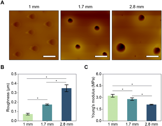
Surface mechanical properties such as roughness and Young's modulus significantly impacted the sensing performance of the sensor. Therefore, they were critical factors that had to be carefully considered in sensor design. To observe the mechanical properties of the surface of the microwell according to membranes thickness, surface morphologies of microwells membranes were visualized and subjected to AFM analysis (Fig. 4). In Fig. 4A, the smoothest surface was observed for the 1 mm membrane, while values of roughness and Young's modulus of microwell membranes increased with increasing thickness. In Fig. 4B, average values of roughness for microwell membranes were 0.07 ± 0.01 μm, 0.17 ± 0.01 μm, and 0.35 ± 0.04 μm for membrane thicknesses of 1, 1.7, and 2.8 mm, respectively. As the thickness of the microwell membrane increased, the value of Young's modulus decreased as shown in Fig. 4C. Young's moduli calculated from force–displacement (F–D) curves obtained from AFM were 3.22 ± 0.18 MPa, 2.80 ± 0.16 MPa, and 2.09 ± 0.05 MPa for membrane thicknesses of 1 mm, 1.7 mm, and 2.8 mm, respectively.
As the number of pores on the surface of the microwell membrane increased, the surface stress decreased, potentially leading to a reduction in roughness. On the other hand, an increase in microwell size resulted in an increase of empty space below the surface, contributing to a decrease in the Young's modulus value of the microwell membrane.
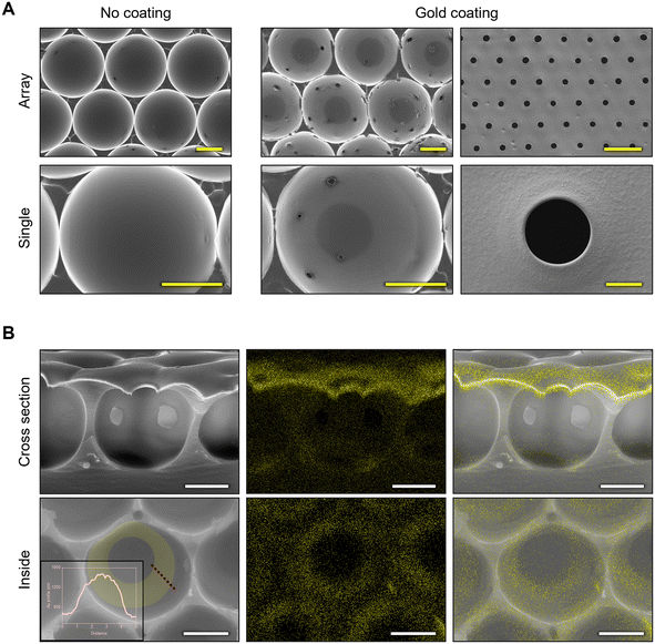
To allow for electrical properties, the microwell membrane was coated with gold at a thickness of 300 nm via the E-beam process. Fig. 5A shows microwells with and without gold coating. The surface of the microwell membrane including the slightly convex hole shape was uniformly coated with gold. After gold coating, the membrane surface and the inside of the microwell were entirely coated with gold except for the bottom of the microwell. Notably, a donut-shaped pattern was observed inside the microwell. As shown in Fig. 5B, yellow dots indicated positions of gold particles, which coated not only the surface, but also the inside of the microwell. A donut-shaped pattern was repeatedly confirmed using EDS mapping and line profile analysis of Au element. While gold was deposited using an E-beam, the substrate continued to rotate, resulting in a donut-shaped gold pattern. These elemental analysis results suggest that microwells can exhibit electrical properties from their surfaces to their inside. The donut-shaped gold pattern observed in the microwell arrays could be intentionally utilized to concentrate electric fields or enhance the sensitivity of the sensor in specific regions of the microwell.
Optimization for lambda DNA electrophoresis
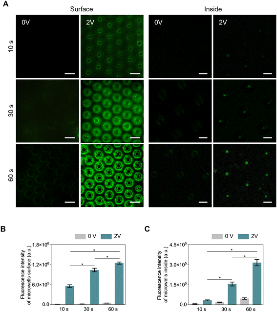
To confirm the applicability of microwells for DNA detection, an electrophoresis test was performed using fluorescently stained lambda DNAs. Initial experiments were conducted to optimize electrical treatment conditions using 2.8 mm microwells, which were expected to have the highest amount of lambda DNA attached due to the highest roughness of 2.8 mm microwells. Fig. 6A shows fluorescence confocal images of lambda DNAs attached to the surface and inside of microwells according to electrophoresis time. At a voltage of 0, there was almost no lambda DNA attached to the microwell. On the other hand, at a voltage of 1 volt for 60 s, DNA detection was only observed on the surface of microwells, suggesting that a voltage of 1 volt was insufficient to generate an electric field to capture DNA inside microwells (Fig. S4†). As the time of electrical treatment increased, the intensity of fluorescence was proportionally increased at a voltage of 2. After 30 seconds of treatment, lambda DNAs were observed to be densely and partially attached to the edge of the microwell hole on the surface. At 60 seconds, more uniform and larger amounts of lambda DNAs were found in microwell holes compared to 30 seconds. To minimize DNA damage associated with increased voltage, a voltage of 2 volts was applied, at which stable DNA attachment was observed. No further increase in voltage was implemented.33,34 Additionally, to investigate the influence of nonspecific interaction in DNA sensing, blank sample experiments (only fluorescent dye without DNA) were conducted. As shown in Fig. S5,† no significant fluorescence intensity was observed in blank samples compared to the 8.6 ng μL−1 DNA concentration sample at a voltage of 0. In contrast, the fluorescence intensity of DNA at a concentration of 8.6 ng μL−1 increased by 28.7-fold at a voltage of 2 volts compared to that of DNA at the same concentration with a voltage of 0 V, which demonstrated that DNA detection was controlled by electrical characteristics.The fluorescence image of the microwell inside indicated that lambda DNA had entered into the microwell along the electric field. The absence of DNA detection on the microwell surface was attributed to the electric field concentration caused by the edge effect at the entrance and the donut-shaped gold pattern formed inside the microwell.
The attachment of lambda DNA was investigated again through FE-SEM analysis. Fig. S6† shows lambda DNAs attached inside microwells according to treatment times of 10, 30 and 60 seconds. Compared to the smooth surface inside the microwell at 0 seconds, increased electrical treatment time resulted in attachment of more lambda DNAs and a rougher surface.
The fluorescence intensity of each microwell was quantitatively analyzed. As shown in Fig. 6B and C, a signal increase was observed with increasing treatment time at both the surface and inside of microwells. Overall, there was almost no signal at 0 voltage compared to 2 voltages. At 60 seconds on surfaces of microwells, the fluorescence intensity was significantly increased by 1.87-fold or 2.25-fold compared to that at 30 seconds or 10 seconds, respectively. The fluorescence intensity inside the microwells increased by 4.75-fold and 9.67-fold at 30 and 60 seconds, respectively, compared to 10 seconds. At 60 seconds, microwells showed the highest fluorescence intensity which could be explained by the highest number of attached lambda DNAs.
The reproducibility of the sensor was investigated through RSD values according to electrical treatment time (Table 1). As the electrical treatment time increased, the RSD value decreased, indicating good reproducibility of the sensor for detection.35 These results suggested that the saturation of DNA attachment occurred at 60 seconds, resulting in a consistent amount of DNA bound to microwells. Therefore, 60 seconds was selected as the electrical treatment time condition.
| 2.8 mm microwells | Sample number | Relative standard deviation (RSD) | ||||
|---|---|---|---|---|---|---|
| 1 | 2 | 3 | 4 | 5 | ||
| 10 s | 484![[thin space (1/6-em)]](https://www.rsc.org/images/entities/char_2009.gif) 014 014 |
575![[thin space (1/6-em)]](https://www.rsc.org/images/entities/char_2009.gif) 342 342 |
576![[thin space (1/6-em)]](https://www.rsc.org/images/entities/char_2009.gif) 267 267 |
566![[thin space (1/6-em)]](https://www.rsc.org/images/entities/char_2009.gif) 310 310 |
571![[thin space (1/6-em)]](https://www.rsc.org/images/entities/char_2009.gif) 557 557 |
7.16% |
| 30 s | 952![[thin space (1/6-em)]](https://www.rsc.org/images/entities/char_2009.gif) 225 225 |
1![[thin space (1/6-em)]](https://www.rsc.org/images/entities/char_2009.gif) 027 027![[thin space (1/6-em)]](https://www.rsc.org/images/entities/char_2009.gif) 868 868 |
1![[thin space (1/6-em)]](https://www.rsc.org/images/entities/char_2009.gif) 064 064![[thin space (1/6-em)]](https://www.rsc.org/images/entities/char_2009.gif) 613 613 |
1![[thin space (1/6-em)]](https://www.rsc.org/images/entities/char_2009.gif) 099 099![[thin space (1/6-em)]](https://www.rsc.org/images/entities/char_2009.gif) 475 475 |
1![[thin space (1/6-em)]](https://www.rsc.org/images/entities/char_2009.gif) 040 040![[thin space (1/6-em)]](https://www.rsc.org/images/entities/char_2009.gif) 589 589 |
5.27% |
| 60 s | 1![[thin space (1/6-em)]](https://www.rsc.org/images/entities/char_2009.gif) 275 275![[thin space (1/6-em)]](https://www.rsc.org/images/entities/char_2009.gif) 351 351 |
1![[thin space (1/6-em)]](https://www.rsc.org/images/entities/char_2009.gif) 286 286![[thin space (1/6-em)]](https://www.rsc.org/images/entities/char_2009.gif) 124 124 |
1![[thin space (1/6-em)]](https://www.rsc.org/images/entities/char_2009.gif) 225 225![[thin space (1/6-em)]](https://www.rsc.org/images/entities/char_2009.gif) 403 403 |
1![[thin space (1/6-em)]](https://www.rsc.org/images/entities/char_2009.gif) 220 220![[thin space (1/6-em)]](https://www.rsc.org/images/entities/char_2009.gif) 054 054 |
1![[thin space (1/6-em)]](https://www.rsc.org/images/entities/char_2009.gif) 220 220![[thin space (1/6-em)]](https://www.rsc.org/images/entities/char_2009.gif) 558 558 |
2.61% |
Assessment for lambda DNA detection attached to microwells
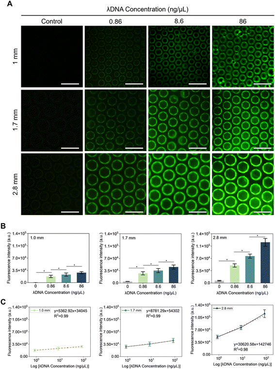
To verify the feasibility of the microwell biosensor for DNA detection, fluorescence examination was carried out using three concentrations of lambda DNA: 0.86, 8.6, and 86 ng μl−1. Fig. 7A presents fluorescence images of the microwell as a platform for sensing attached lambda DNAs at different concentrations after electrophoresis for 60 seconds. It was observed that the fluorescence intensity gradually increased with increasing concentration of lambda DNAs.Additionally, to verify the effectiveness of the microwell structure, lambda DNA detection was performed on flat PDMS (in Fig. S7†). DNA was attached unevenly on the surface of flat PDMS. As a result, no significant difference in fluorescence intensity was observed between DNA concentrations of 0 and 0.86 ng μL−1 on flat PDMS. At a DNA concentration of 0.86 ng μL−1, the RSD value was 62.9%, indicating poor reproducibility on flat PDMS. These results suggest that the structure of numerous individual microwells significantly contributes to enhancing the accuracy of DNA sensing.
Fluorescence intensities of experimental and control groups were compared. Results are shown in Fig. 7B. The control group of microwells had no DNA while the experimental group had DNA. For uniform measurement, the fluorescence intensity of the middle part of the microwell was measured. The fluorescence intensity for lambda DNA at a concentration of 8.6 ng μl−1 significantly increased by 1.30, 1.28, and 1.53-fold with 1, 1.7, and 2.8 mm microwells, respectively. For lambda DNA at 86 ng μl−1, the fluorescence intensity was significantly elevated by 1.24, 1.28, and 1.5-fold compared to that for lambda DNA at 8.6 ng μL−1 with 1, 1.7, and 2.8 mm microwells, respectively. The enhancement of fluorescence intensity observed with the 2.8 mm microwell compared to 1 mm and 1.7 mm microwells was due to the greater surface roughness, which enhanced electric fields, thereby enhancing the potential for DNA attachment.20,36 Results of linear regression analysis for 0 to 86 ng μL−1 of lambda DNA in 1.0, 1.7, and 2.8 mm microwells showed the following equations: FL = 5362.92![[thin space (1/6-em)]](https://www.rsc.org/images/entities/char_2009.gif) log
log![[thin space (1/6-em)]](https://www.rsc.org/images/entities/char_2009.gif) C (ng μL−1) + 34
C (ng μL−1) + 34![[thin space (1/6-em)]](https://www.rsc.org/images/entities/char_2009.gif) 045 with a correlation of 0.99, FL = 8781.29
045 with a correlation of 0.99, FL = 8781.29![[thin space (1/6-em)]](https://www.rsc.org/images/entities/char_2009.gif) log
log![[thin space (1/6-em)]](https://www.rsc.org/images/entities/char_2009.gif) C (ng μL−1) + 54
C (ng μL−1) + 54![[thin space (1/6-em)]](https://www.rsc.org/images/entities/char_2009.gif) 302 with a correlation of 0.99, and FL = 30
302 with a correlation of 0.99, and FL = 30![[thin space (1/6-em)]](https://www.rsc.org/images/entities/char_2009.gif) 620.58
620.58![[thin space (1/6-em)]](https://www.rsc.org/images/entities/char_2009.gif) log
log![[thin space (1/6-em)]](https://www.rsc.org/images/entities/char_2009.gif) C (ng μL−1) + 142
C (ng μL−1) + 142![[thin space (1/6-em)]](https://www.rsc.org/images/entities/char_2009.gif) 746 with a correlation of 0.98 (Fig. 7(C)). Meanwhile, LODs of lambda DNA in 1.0, 1.7, and 2.8 mm microwells were 0.05, 0.06, and 0.1 ng μL−1, respectively, with 1.0 mm microwells exhibiting the lowest LOD value, while 2.8 mm microwells showing the highest LOD value. This could be explained by the fact that as the membrane thickness increased, the sizes of microwells also increased, while the number of microwells decreased, resulting in a reduced detection area for DNA capture.
746 with a correlation of 0.98 (Fig. 7(C)). Meanwhile, LODs of lambda DNA in 1.0, 1.7, and 2.8 mm microwells were 0.05, 0.06, and 0.1 ng μL−1, respectively, with 1.0 mm microwells exhibiting the lowest LOD value, while 2.8 mm microwells showing the highest LOD value. This could be explained by the fact that as the membrane thickness increased, the sizes of microwells also increased, while the number of microwells decreased, resulting in a reduced detection area for DNA capture.
For biomedical applications, platforms that can enhance reproducibility and enable high-throughput screens (HTS) are essential. Therefore, the reproducibility of DNA detection was evaluated with a substantial number of precisely fabricated microwells. The relative standard deviation (RSD) was determined to assess the performance of these microwells as biosensors for DNA detection, with variations in microwell size (Table 2). Fluorescence intensity measurements were obtained from 25 microwells randomly selected from five samples. At a DNA concentration of 0.86 ng μl−1, the 2.8 mm microwell demonstrated an RSD of 1.85%, markedly lower than RSDs observed for microwells with other sizes. Results of comparing various fabrication methods in previously reported studies and their respective RSD values are shown in Table S1.† The proposed microwell sensor demonstrated a significantly lower RSD value than previously reported methods, indicating its superior reproducibility and consistency for DNA detection.
| 0.86 ng μL−1 concentration | Sample number | Relative standard deviation (RSD) | ||||
|---|---|---|---|---|---|---|
| 1 | 2 | 3 | 4 | 5 | ||
| 1.0 mm | 26![[thin space (1/6-em)]](https://www.rsc.org/images/entities/char_2009.gif) 237 237 |
27![[thin space (1/6-em)]](https://www.rsc.org/images/entities/char_2009.gif) 382 382 |
28![[thin space (1/6-em)]](https://www.rsc.org/images/entities/char_2009.gif) 939 939 |
29![[thin space (1/6-em)]](https://www.rsc.org/images/entities/char_2009.gif) 776 776 |
29![[thin space (1/6-em)]](https://www.rsc.org/images/entities/char_2009.gif) 446 446 |
5.29% |
| 1.7 mm | 44![[thin space (1/6-em)]](https://www.rsc.org/images/entities/char_2009.gif) 596 596 |
43![[thin space (1/6-em)]](https://www.rsc.org/images/entities/char_2009.gif) 863 863 |
46![[thin space (1/6-em)]](https://www.rsc.org/images/entities/char_2009.gif) 806 806 |
46![[thin space (1/6-em)]](https://www.rsc.org/images/entities/char_2009.gif) 480 480 |
45![[thin space (1/6-em)]](https://www.rsc.org/images/entities/char_2009.gif) 051 051 |
2.76% |
| 2.8 mm | 117![[thin space (1/6-em)]](https://www.rsc.org/images/entities/char_2009.gif) 820 820 |
116![[thin space (1/6-em)]](https://www.rsc.org/images/entities/char_2009.gif) 565 565 |
115![[thin space (1/6-em)]](https://www.rsc.org/images/entities/char_2009.gif) 643 643 |
115![[thin space (1/6-em)]](https://www.rsc.org/images/entities/char_2009.gif) 969 969 |
112![[thin space (1/6-em)]](https://www.rsc.org/images/entities/char_2009.gif) 081 081 |
1.85% |
Conclusion
This study demonstrated a novel fabrication method for microwells. It also demonstrates that microwells are a powerful and effective approach for DNA detection as biosensors. The microwell was fabricated by controlling bubbles trapped within a PDMS mixture under high-pressure conditions. This fabrication method represents a simple and cost-effective approach to PDMS microarray production. Sizes and mechanical properties of microwells were measured. The highest roughness and lowest Young's modulus values were observed for the 2.8 mm microwell. Electrophoresis experiments were performed to confirm the potential of the microwell as a DNA sensor. As electrical treatment time increased, the fluorescence intensity increased proportionally. DNA sensing performances of 1, 1.7, and 2.8 mm microwells were evaluated using three different DNA concentrations of 0.86, 8.6, and 86 ng μL−1. In particular, the 2.8 mm microwell showed a greater change in fluorescence intensity depending on DNA concentration compared to the other microwells. The reason was that the 2.8 mm microwell enhanced the electric field by increasing the surface roughness, which improved DNA attachment. Additionally, at a concentration of 0.86 ng μL−1, the RSD was measured for each microwell to assess the producibility of the microwell as a DNA sensor. RSD values were 5.29, 2.76, and 1.85% for 1, 1.7, and 2.8 mm microwells, respectively. These results indicated that our proposed microwell exhibited efficient performance and good reproducibility. We believe that the developed microwells could be potentially used as a biosensor for a variety of DNA applications. This platform could be extended to detect clinically relevant targets such as viruses, bacteria, and cancer biomarkers.Data availability
All data supporting the findings of this study are available within the paper and its ESI.† All data reported in this paper will be shared by the corresponding author upon reasonable request.Author contributions
Yeongseok Jang: writing – original draft, visualization, methodology, investigation, formal analysis, data curation, conceptualization; Jonghyun Oh: writing – review & editing, supervision, funding acquisition.Conflicts of interest
There are no conflicts to declare.Acknowledgements
This work was supported by grants (grant numbers: NRF-2023R1A2C1006145 and 2022R1C1C2006901) of the National Research Foundation of Korea (NRF) funded by the Ministry of Science and ICT, Republic of Korea.References
- A. A. Manzoor, L. Romita and D. K. Hwang, Can. J. Chem. Eng., 2021, 99, 61–96 CrossRef CAS.
- K. Kim, S.-H. Kim, G.-H. Lee and J. Y. Park, Biofabrication, 2018, 10, 045003 CrossRef PubMed.
- C.-T. Chen, F.-G. Tseng and C.-C. Chieng, Sens. Actuators, A, 2006, 130, 12–19 CrossRef.
- J. Li, Y. Wang, Z. Lu and M. Chan, Anal. Chim. Acta, 2006, 571, 34–39 CrossRef CAS PubMed.
- J. Wang, L. Du, Y. Han, D. Zhang and D. Jing, Lab Chip, 2023, 23, 5165–5172 RSC.
- S. Roy, J. H. Soh and Z. Gao, Lab Chip, 2011, 11, 1886–1894 RSC.
- T. Jain, A. Papas, A. Jadhav, R. McBride and E. Saez, Lab Chip, 2012, 12, 939–947 RSC.
- J. Y. Park, D. H. Lee, E. J. Lee and S.-H. Lee, Lab Chip, 2009, 9, 2043–2049 RSC.
- T. Liu, M. Winter and B. Thierry, Biomaterials, 2014, 35, 6060–6068 CrossRef CAS PubMed.
- Z. Wang, H. Hu, Y. Wang, Y. Wang, Q. Wu, L. Liu and G. Chen, Biomaterials, 2006, 27, 2550–2557 CrossRef CAS PubMed.
- J. M. Cha, H. Park, E. K. Shin, J. H. Sung, O. Kim, W. Jung, O. Y. Bang and J. Kim, Biofabrication, 2017, 9, 035006 CrossRef PubMed.
- C. H. Kim, I. R. Suhito, N. Angeline, Y. Han, H. Son, Z. Luo and T. H. Kim, Adv. Healthcare Mater., 2020, 9, 1901751 CrossRef CAS PubMed.
- M. Bukenya, J. H. Lee, S. Kalidindi, M. DeCortin, L. Tice, P. J. Yoo and H. Yi, Langmuir, 2021, 37, 1456–1464 CrossRef CAS PubMed.
- C. Chen, V. Rengarajan, A. Kjar and Y. Huang, Bioact. Mater., 2021, 6, 1130–1139 CAS.
- X. Sun, Z. Cui, Y. Liang, C. Duan, H. F. Chan, S. Mao, J. Gu, C. Ding, X. Yang and Q. Wang, Biofabrication, 2023, 15, 035005 CrossRef CAS PubMed.
- H. H. Hwang, S. You, X. Ma, L. Kwe, G. Victorine, N. Lawrence, X. Wan, H. Shen, W. Zhu and S. Chen, Biofabrication, 2021, 13, 025007 CrossRef CAS PubMed.
- E. Behroodi, H. Latifi, Z. Bagheri, E. Ermis, S. Roshani and M. Salehi Moghaddam, Sci. Rep., 2020, 10, 22171 CrossRef CAS PubMed.
- M. A. Nguyen, N. T. Dinh, M. H. Do Thi, D. Nguyen Thi, U. T. Pham, T. Q. Tran, V. M. Nguyen, N. H. Le, D. T. Nguyen and D. T. N. Pham, ACS Omega, 2024, 9, 16949–16958 CAS.
- J. L. Albritton, J. D. Roybal, S. J. Paulsen, N. J. Calafat, J. A. Flores-Zaher, M. C. Farach-Carson, D. L. Gibbons and J. S. Miller, RSC Adv., 2016, 6, 8980–8991 RSC.
- H.-I. Peng, C. M. Strohsahl, K. E. Leach, T. D. Krauss and B. L. Miller, ACS Nano, 2009, 3, 2265–2273 CrossRef CAS PubMed.
- Y. Chen, C. C. Wong, T. S. Pui, R. Nadipalli, R. Weerasekera, J. Chandran, H. Yu and A. R. Rahman, Sens. Actuators, B, 2012, 173, 903–907 CrossRef CAS.
- O. Srivannavit, M. Gulari, E. Gulari, E. LeProust, J. P. Pellois, X. Gao and X. Zhou, Sens. Actuators, A, 2004, 116, 150–160 CrossRef CAS.
- S. Lindström, M. Hammond, H. Brismar, H. Andersson-Svahn and A. Ahmadian, Lab Chip, 2009, 9, 3465–3471 RSC.
- D. K. Wood, D. M. Weingeist, S. N. Bhatia and B. P. Engelward, Proc. Natl. Acad. Sci. U. S. A., 2010, 107, 10008–10013 CrossRef CAS PubMed.
- Y. Liu, S. Jia and L.-H. Guo, Sens. Actuators, B, 2012, 161, 334–340 CrossRef CAS.
- Y. Yang, H. S. Rho, M. Stevens, A. G. Tibbe, H. Gardeniers and L. W. Terstappen, Lab Chip, 2015, 15, 4331–4337 RSC.
- J. Yuan and P. A. Sims, Sci. Rep., 2016, 6, 33883 CrossRef CAS PubMed.
- S. Safdar, K. Ven, J. van Lent, B. Pavie, I. Rutten, A. Dillen, S. Munck, J. Lammertyn and D. Spasic, Biosens. Bioelectron., 2020, 152, 112017 CrossRef CAS PubMed.
- C. D. Ahrberg, J. W. Choi, J. M. Lee, K. G. Lee, S. J. Lee, A. Manz and B. G. Chung, Lab Chip, 2020, 20, 3560–3568 RSC.
- J. Hu, L. Chen, P. Zhang, K. Hsieh, H. Li, S. Yang and T.-H. Wang, Lab Chip, 2021, 21, 4716–4724 RSC.
- J. Shen, J. Zheng, Z. Li, Y. Liu, F. Jing, X. Wan, Y. Yamaguchi and S. Zhuang, Lab Chip, 2021, 21, 3742–3747 RSC.
- Y. Jang, J. Won, Y. Lee, S.-H. Park and J. Oh, Sens. Actuators, B, 2024, 415, 135991 CrossRef CAS.
- W. Meaking, J. Edgerton, C. Wharton and R. Meldrum, Biochim. Biophys. Acta, Gene Struct. Expression, 1995, 1264, 357–362 CrossRef PubMed.
- J. P. Cerón-Carrasco and D. Jacquemin, Chem. Commun., 2013, 49, 7578–7580 RSC.
- V. Vamvakaki, D. Fournier and N. A. Chaniotakis, Biosens. Bioelectron., 2005, 21, 384–388 CrossRef CAS PubMed.
- P. Lazić and B. Persson, Europhys. Lett., 2010, 91, 46003 CrossRef.
Footnote |
| † Electronic supplementary information (ESI) available. See DOI: https://doi.org/10.1039/d4lc00654b |
| This journal is © The Royal Society of Chemistry 2025 |

