Rheological investigations on frequency selective surface carbon composite microwave absorber†
Priyanka
a,
Prashant S.
Alegaonkar
 *a and
Himangshu B.
Baskey
b
aDepartment of Physics, School of Basic Sciences, Central University of Punjab, Bathinda, Punjab 151401, India. E-mail: prashant.alegaonkar@cup.edu.in
bStealth & Camouflage Division, Defence Material Store R & D Establishment, DRDO, Kanpur, UP 208013, India
First published on 10th October 2024
Abstract
A high-performance stealth platform is one of the crucial requirements in defence technology that could practically be realized by building effective microwave frequency selective surface (FSS) absorbers. Herein, we report the design and manufacturing of an absorber by tuning the rheology of cell architecture. Initially, a fan-shaped cell (10.4 mm2) was designed for its surface and bulk rheology. The FSS overlayer composition was investigated using SEM, EDX, and XRD and tuned for 0.25% carbon: 1.5% silver to achieve the ink resistivity ∼255 Ω □−1. The bulk rheology was optimized for air (Roha) spacer (thickness ∼2.8 mm), interlayer dielectrics (0.2 mm each), carbon composition (5%), and cell dimension (10.2 mm). Analyses are presented for absorption loss (RC, dB), bandwidth (GHz), resonance dispersion, and constitutive (ε, μ) parameters, compounded with an equivalent circuit model with the settings R = 273.55 Ω, L = 2.25 nH, C = 0.057 pF and the Fabry–Perot reactance mode@10 GHz. The bi-modal response was investigated for induced polarization, electromagnetic fields, volume power distribution, and angular (Θ = 0°–50°) and rotational stability (Φ = 0°–90°) against TE/TM incidences. The FSS pattern was implemented using a screen printing technique to fabricate a prototype absorber and subjected to the free space measurements in an anechoic chamber. The prototype behaviour was found to be commensurate with the simulated performance, thereby achieving a figure of merit of RC ∼−25 dB@10 GHz, accessible bandwidth 4 GHz (in X band) by using the thickness of 0.057 λ0. Details are presented in this study.
New conceptsInteraction of electromagnetic (EM) signals with a finite-dimensional object is of great tactical importance. Strategically, achieving low observability to the target could be a disruptive act for the enemy state. Conventional coatings in the form of EM shielding were a popular route. However, advancements in radar and surveillance capabilities have driven new pathways for developing shielding, camouflage, and stealth technology. Stealth is an electronic countermeasure that combines the geometry and absorption properties of the military platform. Traditional shields offered a number of challenges such as bandwidth, stability, payload, and service backup. Herein, we proposed an idea of eliminating signature of the target, thereby erasing the echo of the incident signal. The proposed absorber is designed analog to a passive power circuit, capable of transferring maximum incident power. Absorber architecture has been discussed for its texture and rheology, including pattern modelling, material choice, and structure. Field response in terms of bi-modal stability, power, charge distribution, rotational invariance, etc., has been presented. Analysis of the simulated prototype performance has been discussed in light of the figure of merit achieved for the designed absorber. |
1. Introduction
Electromagnetic (EM) absorbers are game-changers in various fields due to their unparalleled ability to manipulate the EM field. They have been receiving widespread attention due to their incredible potential in diversified technologies such as wireless communication and networks, sensors,1 electromagnetic interference (EMI) shielding,2 energy harvesting components, and stealth. Among them, stealth technology is modern combat warfare in which military aircraft, uninhabited air vehicles, warships, rocket launcher platforms, etc., have been made less observable, thereby reducing the radar signature3,4 or remaining low observable from foe radar systems. A number of research and development attempts were made, such as radar-absorbing structures (RASs)5,6 and coating in the form of radar-absorbing materials (RAMs).7,8 These techniques involved the absorption of EM radiation that led to the stealth and shield technology. RAM is associated with the shape of the military platforms and the thickness of the coating adaptable for onboard systems. However, they have inherent limitations in terms of ware/tare, narrow bandwidth, high payload, post-deployment service backup and load bearing, in contrast to RAS.9–11 Thus, RAS is a kind of composite material that integrates the structural and functional properties of an absorption coating. In its traditional format, laminated, porous, and honeycomb structures were the basis for such a class of materials. There are a number of reports in the literature on laminated ferrites and mesoporous carbon materials12,13 integrated with various designs such as Salisbury14 and Jaumann absorbers.15 A typical Salisbury design comprises a resistive sheet of thickness λ/4 placed on a metallic ground plane, whereas, Jaumann consists of a multi-layered resistive sheet architecture to achieve broadband absorption. The reported coatings were found to be cost-effective, lightweight, ecological and compounded with a user-friendly design. However, they offered a significant challenge in terms of bandwidth, thicknesses, and consequently enhancing the payload that led to the limitations on implementing them for practical purposes.In this context, there is an emergence of a new class of synthetic material as an effective absorber. The proposed absorber has a frequency selective characteristic, which comes via designing a peculiar metasurface pattern. Such an absorber is called a frequency selective surface (FSS) absorber. It is an artificially engineered material block that possesses exotic EM properties such as negative permittivity,16 permeability,17 and refractive index.18 FSS absorber scatters the incident signals in an unusual fashion. They are thin, lightweight, mouldable, and conformal, and encompass higher bandwidths with tuneable resonance characteristics to achieve high absorption performance. They are electronic analogs of the PCB-based RLC circuitry with tunned gain parameters.
Ghosh et al. demonstrated an ultra-thin, symmetric, concentric ring, having a bandwidth of 1.15![[thin space (1/6-em)]](https://www.rsc.org/images/entities/char_2009.gif) GHz from 9.50–10.50
GHz from 9.50–10.50![[thin space (1/6-em)]](https://www.rsc.org/images/entities/char_2009.gif) GHz with 96% and 92.5% resonant absorptivity.19 Xu et al. demonstrated the absorber based on the ITO square cut pattern that was capable of absorbing power of more than 90% at a resonant frequency of 17.5 GHz in 8–20 GHz.20 Cheg et al. developed a three-layer square resistive metamaterial having an absorption bandwidth of 156.7% in 4.73–39.04 GHz under TE and TM configurations.21 Similarly, Nguyen et al. proposed a broadband metamaterial absorber with eight resistive arm cells possessing a minimum 90% absorption in 8–13 GHz with good angular stability.22 Tayde et al. presented a polarization-insensitive broadband multilayered resistive absorber with −10 dB reflection loss in 2–18 GHz having a sample thickness of 0.082λL (λL is corresponding to the lowest operating frequency).23 After this Wang et al. demonstrate a flexible and broadband carbon-based resistive frequency selective surface (RFSS) with −10 dB reflection loss in 7.1–35.4 GHz having a sample thickness of 5.5 mm.24 Wang et al. proposed a glass fiber composite and multilayer FSS that exhibits −10 dB loss in 8–18 GHz having a sample thickness of 3.5 mm.25 In a similar fashion Kundu et al., Qu et al., and Luo et al. have also demonstrated resistive pattern-based absorbers.26–28 P. Tiwari et al. also demonstrate a metasurface absorber with 20 dB absorptivity in 10.5–19.5 GHz with 3.2 mm thickness possessing angular stability of up to 40°.29 In general, research studies have demonstrated absorber designs that reduce reflectivity by 10 dB, which is not sufficient for real-time strategic applications. Few research studies have reported microwave absorptivity of 20 dB across some frequencies, however, they have some inherent limitations. Hence, in this work, we have demonstrated composite having 20 dB microwave absorption in the X band region along with a minimum 10 dB absorptivity in the lower and upper sides of the X band spectrum.
GHz with 96% and 92.5% resonant absorptivity.19 Xu et al. demonstrated the absorber based on the ITO square cut pattern that was capable of absorbing power of more than 90% at a resonant frequency of 17.5 GHz in 8–20 GHz.20 Cheg et al. developed a three-layer square resistive metamaterial having an absorption bandwidth of 156.7% in 4.73–39.04 GHz under TE and TM configurations.21 Similarly, Nguyen et al. proposed a broadband metamaterial absorber with eight resistive arm cells possessing a minimum 90% absorption in 8–13 GHz with good angular stability.22 Tayde et al. presented a polarization-insensitive broadband multilayered resistive absorber with −10 dB reflection loss in 2–18 GHz having a sample thickness of 0.082λL (λL is corresponding to the lowest operating frequency).23 After this Wang et al. demonstrate a flexible and broadband carbon-based resistive frequency selective surface (RFSS) with −10 dB reflection loss in 7.1–35.4 GHz having a sample thickness of 5.5 mm.24 Wang et al. proposed a glass fiber composite and multilayer FSS that exhibits −10 dB loss in 8–18 GHz having a sample thickness of 3.5 mm.25 In a similar fashion Kundu et al., Qu et al., and Luo et al. have also demonstrated resistive pattern-based absorbers.26–28 P. Tiwari et al. also demonstrate a metasurface absorber with 20 dB absorptivity in 10.5–19.5 GHz with 3.2 mm thickness possessing angular stability of up to 40°.29 In general, research studies have demonstrated absorber designs that reduce reflectivity by 10 dB, which is not sufficient for real-time strategic applications. Few research studies have reported microwave absorptivity of 20 dB across some frequencies, however, they have some inherent limitations. Hence, in this work, we have demonstrated composite having 20 dB microwave absorption in the X band region along with a minimum 10 dB absorptivity in the lower and upper sides of the X band spectrum.
The focus of the current communication is to design and manufacture an FSS microwave absorber by tuning its surface and bulk rheological properties. The design of the absorber cell consisted of multi-laminate elements such as a fan-shaped FSS overlayer imprinted onto a glass fabric reinforced plastic (GFRP), Roha air spacer, two carbon composite dielectric interlayers, and a carbon fabric reinforced plastic (CFRP) conducting ground. Initially, the rheology of the FSS overlayer was tuned for resistive carbon ink by varying w/w proportion of carbon (0.25–0.30%) and silver nano-particles (1.0–2.5%). The microstructural analysis was performed using FESEM, EDX, and XRD techniques to optimize the composition at 0.25% carbon and 1.5% silver, thereby, achieving the surface resistivity ∼255 Ω □−1. Following this, the parametric variations were made in laminate elements by varying thickness, composition, and dimensions of the designed cell. Its impact on reflection loss (RC@20 dB), accessible bandwidth (8–12 GHz), resonance dispersion, etc., have been studied to design optimally, superior absorber architecture. The equivalent circuit, constructed using different electromagnetic models, was analyzed for open/short circuit conditions including the performance of constitutive (ε′, ε′′) parameters and the Fabry–Perot reactance mode. Analysis of bi-modal (TE/TM) polarization current, electric/magnetic field, and power densities including mode mapping stability (Θ = 0°–50°) and rotational invariance (Φ = 0°–90°) are presented. The performance of the fabricated prototype vis-à-vis simulated absorber is discussed.
2. Methodology: simulation and fabrication
2.1 Simulation studies
The proposed model consists of a fan-shaped FSS unit cell geometry with dimensions 10.4 mm × 10.4 mm (l × w) imprinted on GFRP and integrated with an air spacer (Roha cell), two lossy dielectric carbon composite and a CFRP conducting ground plane. The structure was simulated using a frequency domain solver by applying periodic boundary conditions along the xy-plane and kept open along the z-direction. The rheology of the unit cell was optimized using the solver. The reflectivity in terms of RC was estimated using eqn (1):30RC = 10![[thin space (1/6-em)]](https://www.rsc.org/images/entities/char_2009.gif) log[1 − |S11|2 − |S21|2] log[1 − |S11|2 − |S21|2] | (1) |
RC = 10![[thin space (1/6-em)]](https://www.rsc.org/images/entities/char_2009.gif) log[1 − |S11|2] log[1 − |S11|2] | (2) |
From the extracted S-parameters, the relative impedance (Z) and refractive index (n) of the medium were calculated using:
 | (3) |
 | (4) |
 | (5) |
| εeff = n × z | (6) |
Once the hybrid absorber design was finalized, the equivalent circuit was simulated using transmission line theory and advanced design system (ADS). Further, the complex permittivity measurements of the interlayer dielectrics were carried out using a vector network analyzer (Model: VNA E8364B) and a free space measurement system (FSMS) setup by subjecting it to a calibration process of through-reflect-line (TRL) protocols. Fig. S1 in the ESI† displays the setup of VNA equipped with horn-shaped transmitter/receiver I/O ports, and sample holder assembly.
2.2 Fabrication of absorber
To establish a correlation between the composite ink micro-structure to their resistive properties, a number of characterization techniques were used to optimize the composition of the overlayers. The analysis was carried out using field emission scanning electron microscopy (FESEM, Model: Merlin Compact) compounded with energy-dispersive X-ray spectroscopy (EDS). For this purpose, the ink material was taken in a micropipette, and the drop was released onto a polished and clean silicon substrate. The sample was dried under normal atmospheric conditions. Prior to imaging, the sample was coated with gold. For bulk analysis, the powder X-ray diffraction technique (XRD, make: PAN Analytical, Model: X’pert) was used to identify the crystallographic phases formed into the ink when mixed with the host polymer matrix to control resistivity.
![[thin space (1/6-em)]](https://www.rsc.org/images/entities/char_2009.gif) δ = 0.0004) and (ii) composite lossy laminates. The lossy laminates were fabricated using conducting carbon black (5% w/w), and epoxy matrix/hardener. Both the filler and polymer matrix were add-mixed thoroughly and sonicated for a period of 20 minutes. The process was carried out to disperse nanofillers homogeneously into the polymer medium. Following this, the prepared slurry was spread onto the glass fabric layer, of thickness 0.1 mm, with the help of a doctor blade. The coating thickness was achieved to be 0.1 mm. The thickness uniformity was confirmed using a micro-meter screw gauge of least count 10 μm. The imprinted FSS overlayer along with the lossy interlayer dielectrics was attached and subjected to the compression moulding stage at a kilogram-force of 10 kgf/10 cm2 for about 2 h at a temperature of 55 °C. Subsequently, the prepared laminates were employed in a post-curing process with the help of a hot air flow oven at 80 °C for 02 h. Following this, the specimens were subjected to an edge-finishing process to achieve the tile dimensions of 208 mm × 208 mm.
δ = 0.0004) and (ii) composite lossy laminates. The lossy laminates were fabricated using conducting carbon black (5% w/w), and epoxy matrix/hardener. Both the filler and polymer matrix were add-mixed thoroughly and sonicated for a period of 20 minutes. The process was carried out to disperse nanofillers homogeneously into the polymer medium. Following this, the prepared slurry was spread onto the glass fabric layer, of thickness 0.1 mm, with the help of a doctor blade. The coating thickness was achieved to be 0.1 mm. The thickness uniformity was confirmed using a micro-meter screw gauge of least count 10 μm. The imprinted FSS overlayer along with the lossy interlayer dielectrics was attached and subjected to the compression moulding stage at a kilogram-force of 10 kgf/10 cm2 for about 2 h at a temperature of 55 °C. Subsequently, the prepared laminates were employed in a post-curing process with the help of a hot air flow oven at 80 °C for 02 h. Following this, the specimens were subjected to an edge-finishing process to achieve the tile dimensions of 208 mm × 208 mm.
3. Results and discussion
The proposed hybrid absorber comprised a multilayered structure with specific constitutive (ε, μ) properties. It has a prime function to absorb and arrest the net incident EM field. To minimize the reflection effects, at the air/absorber interface, the overlayer sheet resistance is essentially tuned closer to the free space microwave impedance. Thus, the rheology of the synthesized ink composite plays a crucial role in the construction of an effective absorber.3.1 Microstructure analysis of FSS overlayer: ink composite rheology
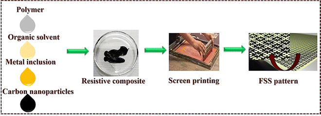
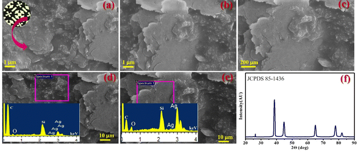
The composition of the carbon nano-particle fillers was kept constant@0.25 w/w%. The silver nano-particle inclusion was varied from 1.0 to 2.5 w/w%. The rheology of 1.5 w/w% composite with surface resistance 255 Ω □−1 showed commensurate absorption performance with that of the simulated FSS overlayer. Fig. 2(a)–(e) shows the recorded surface morphology of the composite ink. Insets in Fig. 2(d) and (e) display the elemental composition of the imprinted material. EDAX spectra of the composition of (a) raw CB, (b) Ag NPs, and (c) ink composite are provided in the ESI† as Fig. S2 including data of atomic% of elements in Table S1 (ESI†). The spectra show the presence of OJ lines associated with carbon, silver, and a fraction of oxygen elements. The presence of oxygen is attributed to a native oxide formed on the surface region of silver nanoparticles. The presence of oxygen could be due to the organic solvent used during the synthesis of the composite. Thus, the rheological analysis revealed that the imprinted material was mainly composed of carbon and silver. In FESEM, the morphology of the composite was seen to be homogenous and uniform. No trace of aggregation of silver or carbon nanoparticles was seen. The carbonaceous material, due to its local covalent bonding environment could offer tuneable electrical resistivity compounded with the conducting silver nano-particles. This could be advantageous to architect a host surface to generate the symmetric patterns of displacement currents. In their interaction with the incident microwave field, the scattered power could be arrested within the hybrid absorber structure. Moreover, due to the homogenous nature of the prepared ink paste the screen printing of the FSS overlayer became easy.Fig. 2(f) shows the recorded XRD spectrum for the material. Two characteristic carbon diffraction reflexes emerged at 2θ ∼ 26.5° and 54.5°. They are assigned to the Miller indices (002) and (004) with a corresponding d–spacing of 3.5 Å and 1.9 Å, respectively.31 The characteristic silver diffraction reflexes were found to emerge at 2θ ∼ 38.2°, 64.1°, 77.5° and 81.3°. These peaks were assigned, respectively, to the Miller indices (111), (220), and (311).32 XRD analysis revealed that the composite has two phases of carbon, one contributing to the sp2-bonded carbon. This phase is rich in electrons to participate in generating displacement current paths. In contrast, the presence of the sp3 phase is mainly responsible for encasing the silver nano-particles to give rise to image charges on their interaction with the incident microwaves.
3.2 Cell design and bulk parameters
The proposed absorber is a multilayered structure, as shown in Fig. 3(a), indicating the cell orientation in the xy plane. The design hierarchy is as follows: an FSS overlayer imprinted onto GFRP (t2 = 0.1 mm, ε = 4.3, tan![[thin space (1/6-em)]](https://www.rsc.org/images/entities/char_2009.gif) δ = 0.01), two lossy dielectric laminates made up of carbon composite (t1 = t3 = 0.2 mm thick), air spacer Roha cell (tv = 2.5 mm) with a CFRP (tg = 0.035 mm) conducting ground. The optimized geometric parameters are displayed in Fig. 3(b), indicating cell dimensions u = v = 1.8, q = r = 1.0, p = 2.0, s = 2.24, L = w = 10.4 (all mm). Fig. 3(c) shows the corresponding color scheme.
δ = 0.01), two lossy dielectric laminates made up of carbon composite (t1 = t3 = 0.2 mm thick), air spacer Roha cell (tv = 2.5 mm) with a CFRP (tg = 0.035 mm) conducting ground. The optimized geometric parameters are displayed in Fig. 3(b), indicating cell dimensions u = v = 1.8, q = r = 1.0, p = 2.0, s = 2.24, L = w = 10.4 (all mm). Fig. 3(c) shows the corresponding color scheme.
 | ||
| Fig. 3 (a) Simulated geometry of the hybrid absorber unit cell, (b) FSS pattern displaying geometrical parameters, (c) color codes representing the structural architecture of the designed absorber. | ||
3.3 Cell rheology: performance optimization
Cell architecture plays an important role in achieving high-performance absorption properties. Table 1 shows rheological changes in unit cells, attributed to the absorption performance in terms of bandwidth, loss, and dispersion of resonance. However, one has to keep in mind that all design parameters cannot have superior absorption characteristics simultaneously. Hence, optimization was performed from the perspective of the overall thickness of the absorber. The bold values in Table 1 show the commensurate design parameters to achieve optimum characteristics. Correspondingly, Fig. S3 is provided in the ESI,† which compliments the data in Table 1.| FSS overlayer resistance | Roha spacer thickness | ||||||
|---|---|---|---|---|---|---|---|
| R s Ω □−1 | Bandwidth GHz@20 dB | Loss RC (dB) | Resonance frequency (GHz) | t v mm | Bandwidth GHz@20 dB | Loss RC (dB) | Resonance frequency (GHz) |
| 235 | 2.7 (X) | 22.3 | 9.6 | 2.7 | 3.8 (X) | 25.1 | 10.3 |
| 245 | 3.3 (X) | 24.0 | 9.8 | 2.8 | 3.9 (X) | 25.5 | 10.1 |
| 255 | 3.8 (X) | 26.0 | 10.0 | 2.9 | 3.7 (X) | 26.4 | 9.7 |
| 265 | 4.0 (X) | 27.7 | 10.4 | 3.0 | 3.7 (C, X) | 26.9 | 9.5 |
| 275 | 4.2 (X) | 31.8 | 10.1 | 3.1 | 3.7 (C, X) | 27.2 | 9.3 |
| Interlayer dielectric composite thickness | |||||||
| t 1 mm | t 3 mm | ||||||
| 0.2 | 4.1 (X) | 26.2 | 10.0 | 0.2 | 4.1 (X) | 26.2 | 10.0 |
| 0.3 | 3.3 (C, X) | 25.7 | 9.2 | 0.3 | 3.4 (C, X) | 25.3 | 9.3 |
| 0.4 | 3.3 (C, X) | 25.7 | 9.2 | 0.4 | 2.9 (C, X) | 24.9 | 8.7 |
| 0.5 | 3.0 (C, X) | 25.7 | 8.9 | 0.5 | 2.6 (C, X) | 24.4 | 8.2 |
| Unit cell size (L) mm | wt% of carbon in interlayer composite | ||||||
| 10.1 | 2.8 (X) | 21.8 | 10.3 | 5% | 4.1 (X) | 26.2 | 10.0 |
| 10.2 | 3.4 (X) | 23.2 | 10.2 | 10% | 2.6 (C, X) | 22.7 | 8.9 |
| 10.3 | 3.6 (X) | 24.3 | 10.1 | 15% | — | 19.4 | 7.6 |
| 10.4 | 4.1 (X) | 26.2 | 10.0 | — | — | — | — |
3.4 Equivalent circuit model of the absorber
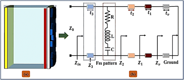
Fig. 4(a) shows the laminated configuration of the absorber cell oriented in the yz plane. Each cell component was transformed into an equivalent resistance (R), inductance (L), and capacitance (C) using the model of the transmission line. The cell was acting as a power circuit that transferred maximum input power into the ground without any losses. The equivalent circuit is shown in Fig. 4(b). For the FSS overlayer, the ink imprints are the R component due to the finite conductivity of the ink material. The contribution of L came from the fan-shaped geometry as well as other cell components. The inter-cell region represents the mutual C between the conjugated area of the pattern. The resistive component functioned as the absorber of the incident power. The C and L contributions emerge from the eddy currents and image charges, respectively, generated due to the induction of the incident power into the absorber.The laminates are displayed in the circuit diagram and represented as the transmission lines of length tv, t1, t2, and t3 with impedances Zv, Z1, Z2, and Z3, respectively. The effective input impedance Zin offered by the absorber is given by:
 | (7) |
3.5 Parametric analysis
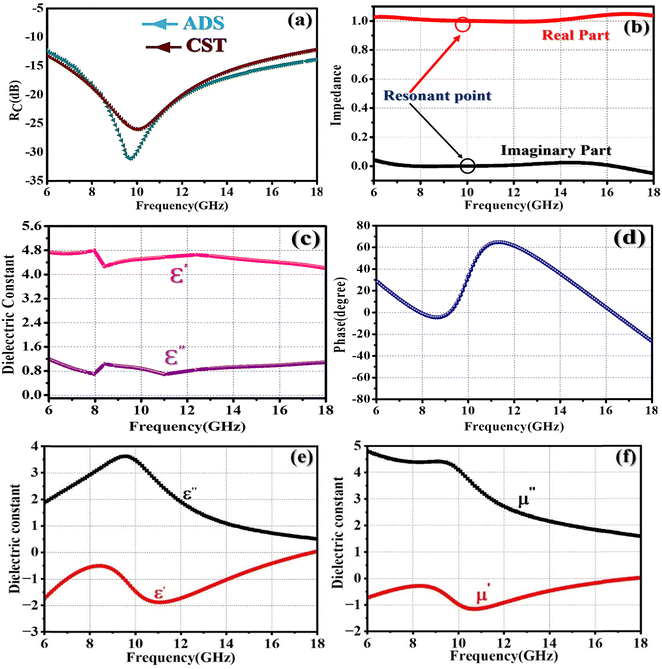
Fig. 5(a) depicts the simulated RC performances using ADS and CST over 6–18 GHz. A minimum 10 dB absorptivity was recorded encompassing C (4–8), X (8–12) and Ku (12–18) bands. Whereas, 20 dB absorptivity was achieved in the X band with a local minimum of 33.5 dB@10 GHz. At the low-frequency region, capacitive coupling dominated over L and R. At resonance, inductive became predominant over R and C. Whereas, at the high-frequency domain resistive coupling was influenced more than L and C. Such a behavior stems from the absorber design. A smaller deviation is noted for the ADS and CST results. By and large, the RC value had reached almost ∼99.9% over the simulated frequency domain. Hence, these variations are negligible. This shows that the effective impedance (Zeff) of the designed absorber is commensurate with the free space impedance (Z0).Fig. 5(b) shows the behaviour of real and imaginary parts of the impedance offered by the absorber. The arrows in the figure indicate the values achieved by the absorber at the resonance frequency. The real and imaginary components of the normalized impedance are nearly one and zero, respectively. This suggests that there is a strong impedance match with free space across the frequency range of 6–18 GHz. As discussed earlier, the absorption properties of the cell depend significantly on the design architecture, typically lossy laminates. Hence parametric analysis of these laminates for their EM properties are discussed in detail. The complex permittivity of the laminate is expressed as εr = ε′ − jε′′, where ε′ = real part, which represents storage of the incident power, and ε′′ = imaginary part indicating dissipation.33Fig. 5(c) shows the variations in complex permittivity for the laminates. The real part was found to be between 4.7–4.2, whereas, the imaginary part was ∼1.1–0.6 over 6–18 GHz. This shows that laminates possess a nine-fold capacity of storage over dissipation of incident power. Fig. 5(d) shows the phase change of the incident signal on an interaction with the cell. At 10 GHz a Fabry–Perot mode was observed. The phase shift was found to be symmetric with respect to the Fabry–Perot mode. The change in the phase is attributed to the capacitive coupling of the unit cell before the resonance. The mode emerges due to the inductive nature and the coupling is capacitive after the surpass of the resonance mode. The analysis is self-consistent with the results presented before. Fig. 5(e) and (f) display the complex permittivity and permeability of the absorber, respectively. The red curve represents the real part, while the black curve represents the imaginary part. The comparison results indicate that the working bandwidth is essentially the same, the real part of ε(ω) and μ(ω) is closer to 0, and hence impedance matching with free space wave is achieved. The imaginary part of the constitutive parameter signifies the loss attributed to the absorber. In 6–18 GHz, the imaginary part is found to be consistently greater than 0, which demonstrates the dominance of the absorption mode.
3.6 Analysis of micro-parameters: current density, electric/magnetic field, and power losses
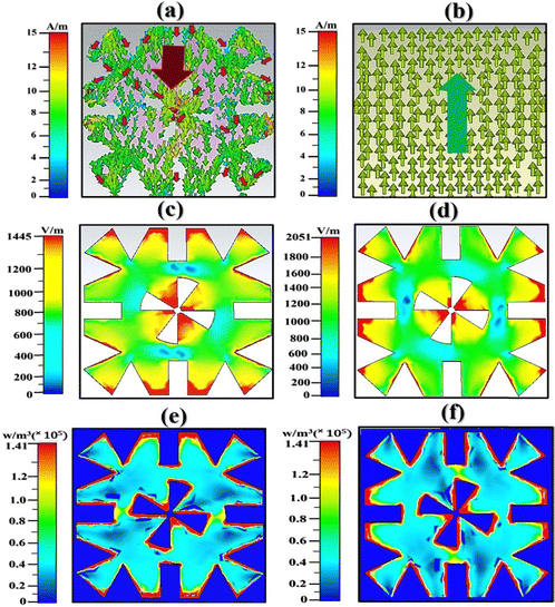
Fig. 6 displays the topological configuration of the cell simulated for the number of micro-parameters. Fig. 6(a) and (b) show induced displacement current at front, and rear surfaces, respectively, for the incident TE mode. On the front surface, currents achieved a value of ∼15 A m−1, typically at the canter region and edges of the fan blades. The direction of the current is semi-curly in nature encompassing the upper portion of the symmetric fan, thereby generating an identical feature spanning the entire tile. There are low current density regions observed at the center of the fan or at the extreme edges. The magnitude of the current density is noted to be 6–10 A m−1 in this region. The effective direction of the induced current density seems to be vectorially orthogonal to the incident TE field. In Fig. 6(b), the rear portion of the absorber is visible in which the current density is found to be uniform across the cell maintaining a magnitude between 6–10 A m−1. The direction vector of the current is opposite to the front surface maintaining the orthogonal nature of coupling with the incident mode. In a similar fashion, surface current density distribution induced by the TM mode was analysed and the data are provided in the ESI† as Fig. S4. In summary, for the TM mode, no peculiar curl-type pattern was observed on the front face. The magnitude of current density was found to be between 8–10 A m−1. For the rear surface, density was found to be in the range of 7–8 A m−1. The direction vectors of the front and rear surfaces were found to be orthogonal and mutually opposite in direction with respect to the incident mode.In a similar manner, surface current density distribution at an angle of incidence 30° and 60° for TE and TM mode are provided in the ESI† as Fig. S5 with detailed description. Fig. 6(c) and (d) show the distribution of the electric field induced by TE and TM modes, respectively. For the TE mode, the field distribution near the fan blades and on the peripheral region of the cell reached a value of 1445 V m−1. In other regions, the field magnitude was found to be lower between 400–600 V m−1. At some places, the field magnitude was found to be moderate between 1000–1200 V m−1. For TM (Fig. 6(d)), the orthogonally symmetric pattern was observed with a diverging field distribution in the region of fan blades. In this region, the field intensity was recorded to be highest between 1600–2051 V m−1. The generated magnetic field distribution for both TE and TM modes is provided in the ESI† as shown in Fig. S6. Summarily, the imprinted overlayer has no magnetic material in its composition. Hence, the magnetic field generated on the top surface is negligible. In most of the regions, the magnitude of the field is almost 0 A m−1. However, in some portions of the cell, the field is seen to be non-zero but has a lowest magnitude of ∼2–4 A m−1. In the absence of any magnetic material, the emergence of the weak magnetic field is attributed to the local loop currents generated due to the magnetic inclusion. This may be due to the presence of impurities in the resistive ink. In a similar fashion, one can see the distribution of power across the unit cell for TE and TM modes displayed in Fig. 6(e) and (f), respectively. For both modes, the geometrical edges present in the unit cell in the form of fan blade and perimeter are the major sources of high-power dissipation of the magnitude 1.2–1.4 × 10⁵ W m−3. The electric field and power loss distribution at 30° and 60° of the incidence for both modes is provided in the ESI† as Fig. S7.
3.7 Angular stability and polarisation insensitivity: TE and TM modes
Fig. 7 shows the topology for (a) TE and (b) TM modes at a variable angle Θ = 0 to 50° over 6–18 GHz of the spectral range. Insets show the corresponding vector representation of TE and TM modes. In mapping (a), the spectrum of TE mode is found to be asymmetric encompassing RC levels from −26 to −10 dB. At the resonance frequency, the spectrum shows a Bell-shaped distribution extended over 9–11 GHz with a max Θ = 20°. In this domain, losses are almost −26 dB. The Bell-shaped pattern is found to be grown asymmetrically for larger incident angles (>40°) with RC spanning almost the entire frequency region attaining loss value up to −10 dB. The TM topology displayed in Fig. 7(b) is distinctly different than that of the TE mode. The highest losses were found to be in the region of Θ = 20°–30° centered ∼12 GHz. The cell has a gradient-type response to the TE mode. Moreover, the cell has offered larger stability to TE coupling, bound asymmetrically around the resonance and spanning the entire frequency domain.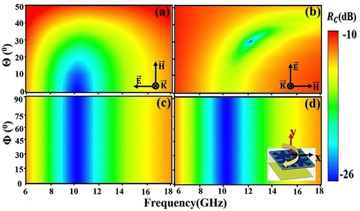 | ||
| Fig. 7 Mapping of RC performance for (a) TE and (b) TM modes at variable angles of incidence Θ = 0°–50°. Topology of cell mapping for (c) TE and (d) TM modes at angular rotation Φ = 0°–90°. | ||
In contrast, the cell has a drifting response to the TM mode. The larger losses are noted in the intermediate Θ region (20°–30°) beyond the resonance limit. This shows that the cell offers an effective absorption of the TE mode with larger angular stability as compared with the TM mode. Fig. 7(c) and (d) show the TE and TM loss spectra, respectively, over 6–18 GHz for Φ = 0°–90°. Inset in (d) shows the rotation of the absorber cell schematically. The loss spectra of both modes are found to be identically symmetric with the highest losses reported near resonance. The bandwidth is almost 2 GHz, centred asymmetrically ∼10 GHz. For larger frequency regions the losses have reached a value of ∼−10 dB. The performance data of RC loss with frequency at the variable angle of incidences Θ = 0°–50° and angular rotation Φ = 0°–90° for TE and TM modes is provided in Fig. S8 in the ESI.†
3.8 Prototype performance
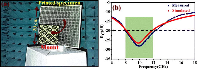
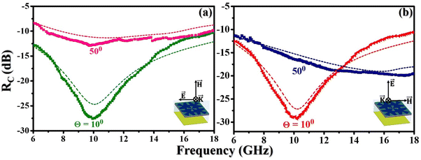
In the above sections, a theoretical construct of cell rheology and simulated absorption performances were discussed. The analysis revealed that the absorption properties could be tuned by controlling the rheology of the cell. Furthermore, the practical implementation of the absorber is described in Section 2.2. The experimental investigations were carried out inside an anechoic chamber, as shown in Fig. 8(a). The measurement setup consisted of a pair of horn antennas with voltage standing wave ratio (VSWR) < 2. In this assembly, the transmitter and receiver antennas were connected to the two ports of a vector network analyzer (Make: Agilent, E 8364B). The absorber was placed at a distance >2D2/λ0 at the required frequency in order to eliminate the near-field scattering effects. Where D is the largest transverse dimension of the transmitting antenna aperture and λ0 is the mean operating wavelength. The data was collected in terms of reflectivity measurements. Initially, measurements were performed on a copper target of identical dimensions to that of the fabricated tile. Following this, the absorber was mounted, and measurements were carried out. The difference in reflectivity response between the copper specimen and the tile was calculated to obtain the actual reflectivity data of the prepared absorber. Fig. 8(b) shows a comparison between measured RC performance with the simulated data. The results are displayed for the mode TE incidence. The measured data is in good agreement with the simulated performance. This shows that it is feasible to implement the designed cell in practice. All the cell parameters are experimentally feasible and up-scalable to realize an actual stealth platform. The fabrication is easy, involves trivial preparation steps, cost- and time-effective. However, a small departure in prototype data has been seen for the simulated RC profile. At low-frequency regions, both profiles match well. The RC deviation of ∼±5% was seen over the X and Ku bands. The resonance peak is in good agreement. This shows that the simulated RLC is commensurate with the experimentally acting RLC patterns. The smaller deviations in X and Ku bands could be attributed to a smaller mismatch in capacitive contribution at low and inductive-resistive action at high-frequency domains.As discussed earlier, mode stability is one of the important parameters to achieve superior absorption characteristics. Fig. 9 shows the bi-modal (TE/TM) performance of the prototype absorber vis a vis the one simulated theoretically. Panel Fig. 9(a) shows behaviour and stability of the TE mode achieved experimentally that agrees effectively with the simulated parameters. The variations in RC and the emergence of absorption peak have a smaller deviation of ∼±5% attributed to the reasons discussed before. In the prototype profile, typically, Θ = 50°, there are certain staggering behaviours in the Ku region, which indicates a weakening of the resistive coupling mode at higher Θ. For the TM mode, displayed in panel Fig. 9(b), similar behaviour between the theoretical and prototype RC performances has been noted. This shows that the prototype absorber is conformally robust in its absorption performance. Table 2 shows a compilation of the performance of relevant absorbers that exist in the literature vis-à-vis current work.
| Ref. | Architecting technique | Structure | Frequency (GHz) | Loss (dB) | Fractional bandwidth (%) | Thickness (mm) | Angular stability |
|---|---|---|---|---|---|---|---|
| a Current work. | |||||||
| 25 | Screen printing | Square patch | 08–18 | 10 | ∼77 | 3.3 | — |
| 26 | Screen printing | Resistive pattern | 03–12 | 10 | 120 | 8 | 0°–45° |
| 27 | Screen printing | Square strips | 04–12 | 10 | 130 | — | 0°–40° |
| 29 | Screen printing | Square layers | 10.5–19.5 | 20 | 60 | 3.4 | 0°–40° |
| 34 | 3-D printing | Honeycomb | 5.52–16.96 | 10 | ∼102 | 5.5 | 0°–45° |
| 35 | Screen printing | Hexa-pattern | 08–18 | 10 | 76 | 1.9 | 0°–60° |
| 36 | Lumped resistor | I-shaped | 08–12 | 20 | 40 | 4.5 | 0°–45° |
| 37 | Screen printing | Double I-shaped | 03–18 | 10 | ∼141 | 7.2 | 0°–45° |
| Screen printing | Fan-shaped | 06–18 | 10 | ∼113 | 3.2 | 0°–50° | |
| 08–12 | 20 | 40 | |||||
Data shows that the current absorber is superior in its design in terms of losses, geometric thickness, and angular stability compounded with broadband performance.
4. Conclusions
We demonstrated the development of a prototype microwave absorber (dimension ∼208 mm2) with a high-performance scattering characteristic. Its unit cell comprises a resistive FSS overlayer (255 Ω □−1) having a fan-shaped topology imprinted onto GFRP laminate (thickness ∼0.2 mm). The overlayer was cascaded to a Roha air spacer (∼2.8 mm), two interlayer dielectrics carbon composites (each ∼0.2 mm), and CFRP ground. The cell design was optimized for its surface and bulk rheology. Its equivalent circuit analysis showed the emergence of a band-symmetric Fabry–Perot reactance mode at 10 GHz with maximum power transfer and zero load resistance tuned for R = 273.55 Ω, L = 2.25 nH, and C = 0.057 pF. The cell is capable of storing ten folds of incident microwave power over absorption. Thus, the fabricated absorber had a loss characteristic of >10 dB over 6–18 GHz and >20 dB in the X band region. It has a slim configuration ∼0.057 λ0 with FBW 113%@10 dB and 40%@20 dB, having angular stability of up to ∼50° and polarization insensitivity of ∼90°. The cell generates displacement currents and image charges due to the fan-shaped geometry, which is responsible for sinking a large amount of power ∼1.3–1.4 × 10⁵ W m−3 at the centre and edges of the blade. The induced polarization currents were found to be upper-bounded and semi-curly in nature at the front and continuous at the rear end of the cell. The field vectors were found to be oriented opposite and have an impact on the locking of the mode of the incident power. In the mode mapping analysis, the TE spectrum showed a strong Gaussian-type coupling with loss centred at 10 GHz (>−25 dB) and bandwidth ∼4 GHz compounded with a gradual increase in the angle of incidence. Whereas, TM was found to be weakly coupled with a skewed lossy band and shifted towards 11.5–12 GHz having maxima near 20°–30°. The bi-modal angular stability spectra, at the resonance condition were found to be maximum (>−20 to −25 dB) and possess a gradient-type lossy dispersion behaviour. The RC performance of the prototype was dictated as per the simulated conditions. The deviation and dispersion in losses were found to be ∼±5% and attributed to the fault-tolerant design of the absorber. The proposed absorber seems to be a well-suited candidate for the stealth platform.Author contributions
Priyanka: implemented work, performed simulations, designed material and performed measurements. HBB: provided experimental facilities and access to the measurements including primary formulation of the problem. PSA: tackled the scientific problems, analysed and interpreted data, including manuscript writing.Data availability
Data will be available upon request to Dr Himangshu B. Baskey (hbbaskey@gmail.com) and Dr Prashant S. Alegaonkar (Prashant.alegaonkar@cup.edu.in).Conflicts of interest
The authors declare no competing interests.Acknowledgements
No funding source is available. The authors are thankful to the Vice-Chancellor and Deans of the Central University of Punjab Bathinda and the Director and Scientist of DMSRDE Kanpur.References
- C. Sabah, F. Dincer, M. Karaaslan, E. Unal, O. Akgol and E. Demirel, Perfect metamaterial absorber with polarization and incident angle independencies based on ring and cross-wire resonators for shielding and a sensor application, Opt. Commun., 2014, 322, 137–142 CrossRef CAS
.
- R. Kumaran, A. V. Kumar, S. Ramaprabhu and V. Subramanian, Absorption-enhanced EMI shielding using silver decorated three-dimensional porous architected reduced graphene oxide in polybenzoxazine composites, New J. Chem., 2021, 45(36), 16939–16948 RSC
.
-
E. F. Knott, J. Shaeffer and M. T. Tuley, Radar Cross Section, Artech House, Inc., Norwood, MA, 1993 Search PubMed
.
- C.-Y. Chen, N.-W. Pu, Y.-M. Liu, S.-Y. Huang, C.-H. Wu and M.-D. Ger,
et al., Remarkable microwave absorption performance of graphene at a very low loading ratio, Composites, Part B, 2017, 114, 395–403 CrossRef CAS
.
- A. Shah, A. Ding, Y. Wang, L. Zhang, D. Wang and J. Muhammad,
et al., Enhanced microwave absorption by arrayed carbon fibers and gradient dispersion of Fe nanoparticles in epoxy resin composites, Carbon, 2016, 96, 987–997 CrossRef CAS
.
- M. Bibi, S. M. Abbas, N. Ahmad, B. Muhammad, Z. Iqbal and U. A. Rana,
et al., Microwaves absorbing characteristics of metal ferrite/multiwall carbon nanotubes nanocomposites in X-band, Composites, Part B, 2017, 114, 139–148 CrossRef CAS
.
- T. Wang, P. Wang, Y. Wang and L. Qiao, A broadband far-field microwave absorber with a sandwich structure, Mater. Des., 2016, 95, 486–489 CrossRef CAS
.
- Y. Zhang, Y. Huang, T. Zhang, H. Chang, P. Xiao and H. Chen,
et al., Broadband and tunable high-performance microwave absorption of an ultralight and highly compressible graphene foam, Adv. Mater., 2015, 27(12), 2049–2053 CrossRef CAS PubMed
.
- K.-Y. Park, S.-E. Lee, C.-G. Kim and J.-H. Han, Fabrication and electromagnetic characteristics of electromagnetic wave absorbing sandwich structures, Compos. Sci. Technol., 2006, 66(3–4), 576–584 CrossRef CAS
.
- W.-H. Choi and C.-G. Kim, Broadband microwave-absorbing honeycomb structure with novel design concept, Composites, Part B, 2015, 83, 14–20 CrossRef CAS
.
- M. Chen, Y. Pei and D. Fang, Design, fabrication, and characterization of lightweight and broadband microwave absorbing structure reinforced by two dimensional composite lattice, Appl. Phys. A: Mater. Sci. Process., 2012, 108, 75–80 CrossRef CAS
.
- F. Nanni, P. Travaglia and M. Valentini, Effect of carbon nanofibres dispersion on the microwave absorbing properties of CNF/epoxy composites, Compos. Sci. Technol., 2009, 69(3–4), 485–490 CrossRef CAS
.
- I. Choi and D. Lee, Radar absorbing composite structures dispersed with nano-conductive particles, Compos. Struct., 2015, 122, 23–30 CrossRef
.
- W. W. Salisbury, Absorbent body for electromagnetic waves, US Pat., 259994410, 1952 Search PubMed.
- L. J. Du Toit, The design of Jauman absorbers, IEEE Antennas Propag. Mag., 1994, 36(6), 17–25 Search PubMed
.
- J. B. Pendry, A. Holden, D. Robbins and W. Stewart, Low frequency plasmons in thin-wire structures, J. Phys.: Condens. Matter, 1998, 10(22), 4785 CrossRef CAS
.
- J. B. Pendry, A. J. Holden, D. J. Robbins and W. Stewart, Magnetism from conductors and enhanced nonlinear phenomena, IEEE Trans. Microwave Theory Tech., 1999, 47(11), 2075–2084 CrossRef
.
- J. B. Pendry, Negative refraction makes a perfect lens, Phys. Rev. Lett., 2000, 85(18), 3966 CrossRef CAS
.
- S. Ghosh, S. Bhattacharyya, Y. Kaiprath and K. Vaibhav Srivastava, Bandwidth-enhanced polarization-insensitive microwave metamaterial absorber and its equivalent circuit model, J. Appl. Phys., 2014, 115, 10 Search PubMed
.
- J. Xu, Y. Fan, X. Su, J. Guo, J. Zhu and Q. Fu,
et al., Broadband and wide angle microwave absorption with optically transparent metamaterial, Opt. Mater., 2021, 113, 110852 CrossRef CAS
.
- P. Chen, X. Kong, J. Han, W. Wang, K. Han and H. Ma,
et al., Wide-angle ultra-broadband metamaterial absorber with polarization-insensitive characteristics, Chin. Phys. Lett., 2021, 38(2), 027801 CrossRef CAS
.
- T. T. Nguyen and S. Lim, Design of metamaterial absorber using eight-resistive-arm cell for simultaneous broadband and wide-incidence-angle absorption, Sci. Rep., 2018, 8(1), 6633 CrossRef PubMed
.
- Y. Tayde, M. Saikia, K. V. Srivastava and S. A. Ramakrishna, Polarization-insensitive broadband multilayered absorber using screen printed patterns of resistive ink, IEEE Antennas Wirel. Propag. Lett., 2018, 17(12), 2489–2493 Search PubMed
.
- Y. Wang, C. Huang, J. Peng, L. Yuan, Y. Qi and X. Luo, Flexible and broadband absorbing woven fabric using carbon-based resistive frequency selective surface, Compos. Struct., 2022, 285, 115262 CrossRef
.
- C. Wang, M. Chen, H. Lei, K. Yao, H. Li and W. Wen,
et al., Radar stealth and mechanical properties of a broadband radar absorbing structure, Composites, Part B, 2017, 123, 19–27 CrossRef CAS
.
- D. Kundu, S. Baghel, A. Mohan and A. Chakrabarty, Design and analysis of printed lossy capacitive surface-based ultrawideband low-profile absorber, IEEE Trans. Antennas Propag., 2019, 67(5), 3533–3538 Search PubMed
.
- Z. Qu, J. Hao, H. Jing, Y. Wei, J. Duan and J. Wang,
et al., An ultra-thin ultra-broadband microwave absorber for radar stealth, Adv. Compos. Hybrid Mater., 2022, 5(3), 1778–1785 CrossRef CAS
.
- H. Luo, F. Chen, X. Wang, W. Dai, Y. Xiong and J. Yang,
et al., A novel two-layer honeycomb sandwich structure absorber with high-performance microwave absorption, Composites, Part A, 2019, 119, 1–7 CrossRef CAS
.
- P. Tiwari, S. K. Pathak and V. Siju, Development of Resistive-Ink Based Planar and Conformal Metasurfaces for RCS Reduction, IEEE Access, 2022, 10, 61472–61483 Search PubMed
.
- N. I. Landy, S. Sajuyigbe, J. J. Mock, D. R. Smith and W. J. Padilla, Perfect metamaterial absorber, Phys. Rev. Lett., 2008, 100(20), 207402 CrossRef CAS
.
- A. Radoń and D. Łukowiec, Structure of nanographite synthesised by electrochemical oxidation and exfoliation of polycrystalline graphite, Micro Nano Lett., 2017, 12(12), 955–959 CrossRef
.
- K. Jemal and B. Sandeep, Pola S. Synthesis, characterization, and evaluation of the antibacterial activity of Allophylus serratus leaf and leaf derived callus extracts mediated silver nanoparticles, J. Nanomater., 2017, 2017(1), 4213275 Search PubMed
.
- X. Han, Y. Huang, J. Wang, G. Zhang, T. Li and P. Liu, Flexible hierarchical ZnO/AgNWs/carbon cloth-based film for efficient microwave absorption, high thermal conductivity and strong electro-thermal effect, Composites, Part B, 2022, 229, 109458 CrossRef CAS
.
- S. Ghosh and S. Lim, Perforated lightweight broadband metamaterial absorber based on 3-D printed honeycomb, IEEE Antennas Wirel. Propag. Lett., 2018, 17(12), 2379–2383 Search PubMed
.
- Priyanka, S. Mohanty, P. S. Alegaonkar and H. B. Baskey, Design and Manufacturing of a Hexapattern Frequency Selective Surface Absorber for Aerospace Stealth Application, ACS Appl. Mater. Interfaces, 2023, 15(30), 37107–37115 CrossRef CAS PubMed
.
- A. P. Sohrab and Z. Atlasbaf, A circuit analog absorber with optimum thickness and response in X-band, IEEE Antennas Wirel. Propag. Lett., 2013, 12, 276–279 Search PubMed
.
- Z. Zhang, Y. Xu, L. Yu, J. Li and X. Hou, A Wideband Absorbing Structure Based on Two Different Resistance Layers and a Magnetic Layer, J. Electron. Mater., 2023, 52(2), 1057–1068 CrossRef CAS
.
Footnote |
| † Electronic supplementary information (ESI) available. See DOI: https://doi.org/10.1039/d4mh00993b |
| This journal is © The Royal Society of Chemistry 2025 |

