
 Open Access Article
 This Open Access Article is licensed under a Creative Commons Attribution-Non Commercial 3.0 Unported Licence
Bird's eye inspired hyperuniform disordered TiO2 meta-atom based high-efficiency metalens†
Ohidul
Islam‡
 a,
Dip
Sarker‡
be,
K. B. M. Sharif
Mahmood‡
c,
Joyprokash
Debnath
d and
Ahmed
Zubair
*b
a,
Dip
Sarker‡
be,
K. B. M. Sharif
Mahmood‡
c,
Joyprokash
Debnath
d and
Ahmed
Zubair
*b
aDepartment of Electrical and Computer Engineering, Auburn University, Auburn, USA
bDepartment of Electrical and Electronic Engineering, Bangladesh University of Engineering and Technology, Dhaka, Bangladesh. E-mail: ahmedzubair@eee.buet.ac.bd
cEskayef Pharmaceuticals Ltd, Bangladesh
dDepartment of Electrical and Computer Engineering, University of Central Florida, Orlando, USA
eDepartment of Electrical and Computer Engineering, University of California San Diego, La Jolla, USA
First published on 18th December 2024
Abstract
We proposed an ingenious, highly efficient TiO2 meta-atom (MA)-based near-infrared disordered metalens structure harnessing bird's eye-inspired hyperuniform distribution and analyzed its optical and imaging properties employing the finite-difference time-domain (FDTD) method. The hyperuniform disordered MAs constructed an image at a focal length by engineering the phase shift of transmittance. We obtained a high focusing efficiency of 84.39% at a wavelength of 820 nm for disordered metalens structures. Amazingly, our proposed disordered metalens structures can mimic the optical properties of ordered metalens structures. Similar focusing efficiencies of disordered and ordered metalens structures were found in a wavelength range from 850 to 890 nm due to the long-range periodic properties of hyperuniform disordered structures. The focal length shifts and NAs of disordered metalens structures were comparable to the focal length shifts and NAs of periodic metalens structures in the entire operating region from 770 to 970 nm with a constant FWHM of 1.503 μm. Our proposed structure paves the way for designing new and innovative imaging, sensing, and spectroscopic technologies, such as lidar, medical devices, IR and machine vision cameras, display systems, and holography.
1 Introduction
The consumer electronics, industrial, medical, and automotive industries are increasingly interested in small and light imaging systems.1–3 Dielectric optical lenses are the primary components of these devices that concentrate light. Therefore, it is crucial to create lightweight and minuscule lenses. However, these properties are not easy to obtain utilizing conventional lenses. Dielectric metalenses are small and promising optical components that can manipulate light like conventional optical lenses but are no thicker than a piece of paper.4 Several metalens structures consisting of various materials have been reported experimentally and numerically; some involved dielectrics, while others were made of metal or phase-changing materials.5–7 Metalenses can reduce the size and weight of the optics in the system, which is conducive to many applications, such as lidar for 3D sensing in autonomous vehicles and facial recognition systems, medical devices, surveillance systems, and holography. Metalenses comprising noble metal structures have significant light attenuation due to high visible plasmatic metal loss.6 In contrast, dielectric metalenses hold great promise for achieving high transmission efficiency while minimizing visual reflection.8 Several dielectric materials, such as silicon (Si),4 silicon dioxide (SiO2),9 titanium oxide (TiO2),8 and gallium nitride (GaN),10 have all been utilized to exhibit different types of metalens structures. Among them, TiO2 is a promising material for metalens applications due to its high band gap, excellent transmission efficiency, minimum light absorption, and high refractive index. Numerous TiO2 MA-based metalens structures have been reported experimentally and numerically by harnessing these unique properties.4,8MA structures can be classified into two distinct arrangements: ordered MA structures and disordered MA structures. Most importantly, these structures enhance optical device performance and miniaturization by varying the size, shape, and material composition of MAs. The arrangement of MAs is properly ordered in periodic formations to achieve maximum efficiency in optics. Hence, many optoelectronic devices, such as solar cells,11 LEDs,12 photodetectors,13 polarization-controlling devices,14,15 and sensors,16 can be used with this periodic arrangement. In contrast, MAs are arranged in an aperiodic formation for disordered MA structures. Though several disordered structures exist in nature, these structures rarely exhibit the properties of an ordered structure. The hyperuniform structure, such as the pigment distribution in a chicken's eye, is a rare pattern that acts as an ordered structure in a disordered structure.17 The cone cell distribution of hyperuniform structures can mimic the distribution of periodic structures by increasing the window radius. Thus, this hyperuniform distribution is called long-range periodic disordered distribution. Several investigations were conducted to analyze this disordered pattern theoretically and experimentally for numerous optoelectronic applications, including bandgap engineering,18 waveguides,19 polarizers,20 and topological insulators.21 Recently, researchers reported several TiO2-based metalens studies to enhance performance parameters, such as maximum focusing efficiency, numerical aperture (NA), and full-width half-maximum (FWHM). Wang et al. reported a highly efficient TiO2 MA-based periodic metalens structure; however, the structure comprised four differently shaped MAs to obtain the desired phase, which requires a complex fabrication technique.8 Khorasaninejad et al. designed a narrowband rectangular TiO2 MA metalens structure in the visible wavelength region using the Pancharatnam–Berry phase technique.22 However, the average efficiency was poor without the ability to control light. The problems associated with controlling light can be assuaged by a slanted two-rectangular dielectric structure.23 However, the structure had an efficiency of 20% at 500 nm. All previously reported MA metalenses were designed with ordered structures; however, no disordered MA metalens structure has been proposed yet. Therefore, there is a scope for designing highly efficient disordered MA metalens structures with a flexible fabrication process by taking inspiration from the bird's eye's color-sensitive cone cell distribution.
In this work, we proposed a disordered TiO2 MA metalens structure on a SiO2 substrate harnessing nature-inspired hyperuniform distribution and analyzed the optical imaging performance utilizing the FDTD method. We obtained the transmittance amplitude and phase shift by varying the structural parameters, such as MA height and radius, via parametric sweep. Additionally, the target phase shift and MA radius profiles for the desired focal length of the metalens were calculated. We designed our metalens structure according to the radius and phase profiles and calculated the simulated phase shift. We designed the metalens structure for a focal length of ∼50 μm. We compared the target phase shift with the simulated phase shift of our proposed disordered structure. Moreover, we compared the performance analysis of our proposed disordered metalens structure with the periodic TiO2 MA metalens structure. A high focusing efficiency of 84.39% was obtained at a wavelength of 820 nm for disordered metalens structures. Additionally, similar focusing efficiencies of disordered and ordered metalens structures were found in a wavelength range from 850 to 890 nm due to the long-range periodic properties of hyperuniform disordered structures. Finally, we conducted an extensive comparative analysis between our proposed structure and previously reported metalens structures.
2 Design and methodology
Metalenses comprised meticulously constructed unit cells or MAs with sub-wavelength specifications. Fig. 1(a) depicts the unit cell of the ordered and hyperuniform disordered metalens structures. We utilized a TiO2 nanorod due to its large bandgap, low light absorption, and excellent light transmission efficiency on a glass (SiO2) substrate. We obtained the material properties of TiO2 and SiO2 from Palik.24 We optimized the MA's height, hpillar, and the substrate's height, hsub, to achieve the highest transparent medium. The optimized hpillar and hsub were set to be 1000 and 280 nm, respectively. We varied the width, d, of the MA to obtain the desired phase. We adopted structural parameters using a parametric sweep technique. The unit cell's periodicity, Px = Py, was considered 520 nm for the best outcomes. We developed a phase profile with varying MA radius, d/2, ranging from 50 to 230 nm. We used this phase profile to set MAs accurately to obtain the desired phase at each grid point of the metalens.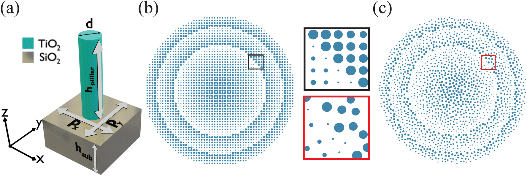 | ||
| Fig. 1 (a) Illustration of the unit cell of TiO2 MAs on a SiO2 substrate. The structural parameters of the unit cell are Px = Py = 520 nm, hpillar = 1000 nm, and hsub = 280 nm. The schematics of (b) periodic and (c) disordered metalens structures. The diameter of the metalens structures was set to be 30 μm. The black and red rectangles illustrate the zoomed-in view of the periodic and disordered metalens structures, respectively. | ||
Fig. 1(b) and (c) depict two-dimensional (2D) illustrations of the spatial distribution of circular ordered and hyperuniform disordered MA metalens structures, where the diameter of the metalens was 30 μm. We adopted a straightforward and conventional approach to building the ordered MA metalens by arranging meta-atoms or unit cells. The MAs in the black and red rectangles illustrate the ordered and disordered distributions of metalenses, respectively. In contrast, Birdson's Poisson disk sampling algorithm was implemented to determine spatial coordinates for the placement of unit cells for our proposed disordered MA metalens structure.25 We generated these structures using predefined desired and unit cell phase profiles. An extensive discussion is provided in the later section. We considered a minimum point-to-point separation distance, m, of 520 nm for our proposed structures, where each cell size was set to be m/2. The selection process of m for our hyperuniform disordered metalens structure is provided in the later section. The grid of our proposed structures was designed so that each cell could occupy just a single element. Hence, the algorithm effectively eliminated any clustering. We provided our generated coordinates of ordered and hyperuniform disordered MA metalens structures in GitHub.26 We can utilize a top-down etching approach to fabricate these ordered and hyperuniform disordered MA structures. Lin et al.27 and Wang et al.8 fabricated a hyperuniform disordered NW laser and an ordered MA metalens structure using the top-down etching approach. They utilized the electron beam lithography technique to grow the MA on the substrate layer, where they employed polymethyl methacrylate (PMMA) and acetone as the photoresist and etchant, respectively. The patterned nanoholes of PMMA could be developed on the substrate. Then, TiO2 can be deposited by using the atomic layer deposition method. This conformal coating fills the patterned gaps in the PMMA nanoholes, forming a precise structure. Finally, a lift-off process to remove the PMMA can be performed by utilizing acetone, which leaves the periodic and disordered TiO2 MA structures on the substrate.
We conducted our study employing the three-dimensional (3D) FDTD method using Ansys Lumerical.28 Additionally, we utilized Python open-source scripting software to generate the coordinates of our ordered and hyperuniform TiO2 MA metalens structures. For unit cell simulation, anti-symmetric and symmetric boundary conditions were applied in the x- and y-directions, respectively. We used 12 steep angle perfectly matched layers (PMLs) in the z-direction. In contrast, we adopted the PML boundary condition in all directions for our ordered and hyperuniform TiO2 MA metalens structures. A transverse magnetic (TM) plane wave was incident normally on the bottom surface of the metalens structures along the z-direction. We used a mesh size of 10 nm in the x- and y-directions to increase the accuracy of the results. We obtained the transmission light's amplitude and phase profile from extracting S parameters.
We analyzed the scalar variance, σ2(R), by varying the window radius, R, for our proposed ordered and hyperuniform disordered structures. In conventional disordered systems, such as liquids and glasses, the scalar variance of MAs inside a d-dimensional observational window follows σ2(R) ∼ Rd. The σ2(R) increased with increasing R. In contrast, when R increased, the variation of σ2(R) was lower compared to Rd for our proposed hyperuniform disordered structure, as shown in Fig. 2(a). Hence, the σ2(R) values of our proposed ordered and hyperuniform disordered structures were closely aligned with each other. Thus, we can model a hyperuniform disordered structure to obtain an ordered structure's properties as it adheres σ2(R) ∼ Rd−1.29 We calculated σ2(R) by using
| σ2(R) = 〈N2(R)〉 − 〈N(R)〉2. | (1) |
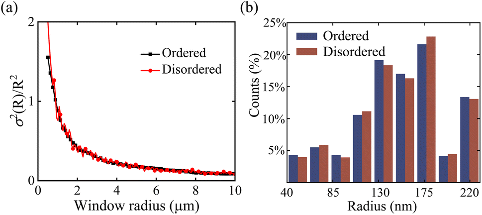 | ||
| Fig. 2 (a) The scaled variance of the number of elements inside a randomly placed observation window for periodic and hyperuniform disordered metalens structures. (b) Percentage distribution of the radius of the MAs of both metalens structures. | ||
3 Results and discussion
3.1 Impact of structural parameters of metalenses
Metalenses comprise numerous tiny elements called MAs. Each MA is engineered to introduce specific phase delays to incoming light. By varying the size, shape, and arrangement of these MAs, metalenses can achieve complex wavefront modulation. This capability allows them to bend light in desired directions, effectively focusing it or creating other optical effects without the need for bulky curved surfaces. Moreover, metalenses can focus light beyond the diffraction limit, which is a significant limitation of conventional lenses. Thus, we need to study the impact of changing structural parameters on transmittance and phase before delving into a full lens study. We varied the structural parameters of the MA, such as radius and height, and analyzed its transmittance and phase, as shown in Fig. 3. A good metalens requires perfect transmittance and phase coverage from 0 to 2π. We tuned the height and radius of the MA to obtain the phase and transmittance; however, controlling both variables was difficult for fabrication and handling codes, increasing the computation requirements. Hence, we fixed one variable while varying the other. Our proposed unit cell exhibited a perfect transmittance and a complete coverage of the phase from 0 to 2π around a MA height of 1000 nm, as shown in Fig. 3(a) and (b). Therefore, we adopted a MA height of 1000 nm for our study.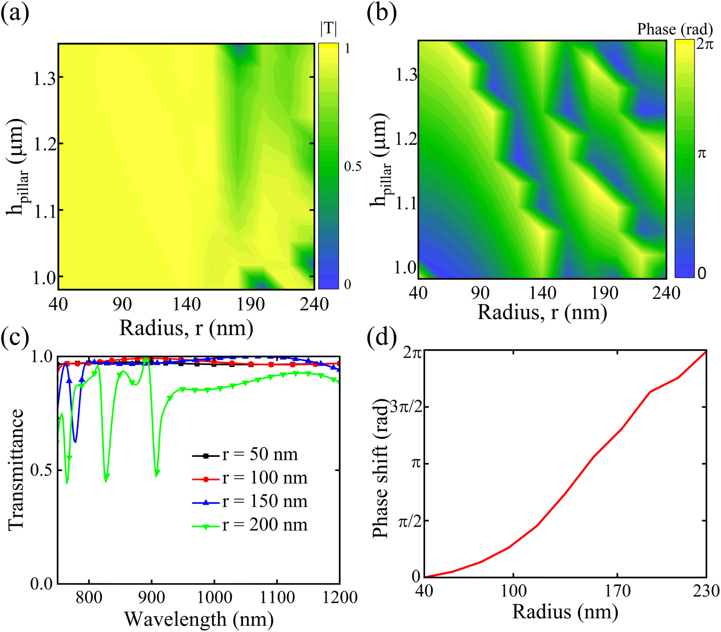 | ||
| Fig. 3 Spatial distributions of (a) the transmission and (b) the phase of a TiO2 MA unit cell with varying height and radius. Here, we considered Px = Py = 520 nm for our study. We varied the MA height from 0.98 to 1.35 μm and the MA radius from 40 to 240 nm, respectively, to cover the phase range from 0 to 2π. (c) Transmission spectra of a unit cell structure for different radii of the MA. Here, the height of the MA was set to be 1 μm. The unit cell exhibited a constant transmittance at 820 and 900 nm for different radii. (d) Numerically calculated phase shifts of a TiO2 MA unit cell with varying MA radius, where the wavelength of incident light was set to be 820 nm. | ||
Moreover, we studied the spatial distributions of the phase by changing the height and radius of the MA. Our proposed unit cell achieved the phase spectrum from 0 to 2π by varying the radius from 40 to 240 nm at a MA height of 1000 nm, as shown in Fig. 3(b). Additionally, we analyzed the impact of the MA radius on the transmittance spectra. We obtained a near-perfect transmittance for different MA radii at 820 and 900 nm, as depicted in Fig. 3(c). When we increased the radius of the TiO2 MA, our meta-atom exhibited reflection at the transmittance dips. The absorptance was negligible for our proposed meta-atoms. Here, we considered 820 nm as our operating wavelength; however, we performed an extensive performance analysis in a broad wavelength range in a later section. We obtained the phase shift from 0 to 2π by varying the MA's radius, as shown in Fig. 3(d), where the height of TiO2 was set to be 1000 nm. This phase profile provided information for placing the MAs to achieve the desired phase of the metalens structure.
3.2 Target phase and radius profiles
We analyzed the desired phase shift of every MA's position on the full structure of the metalens, as shown in Fig. 4(a). We calculated the desired phase shift of the metalens as30 | (2) |
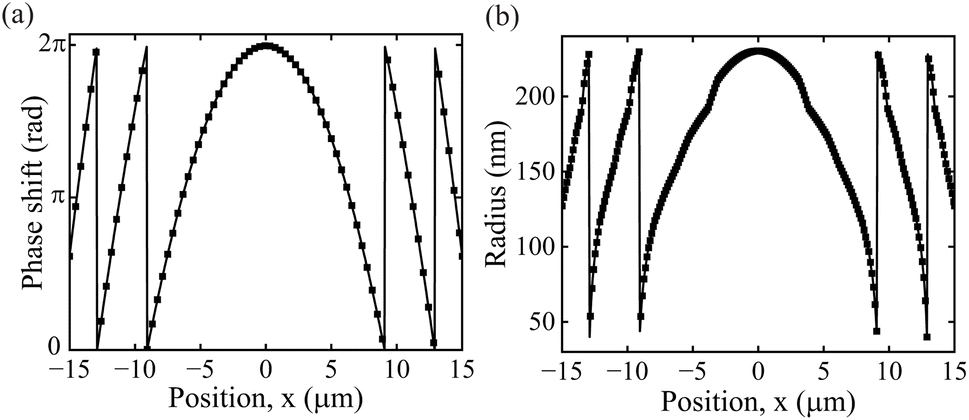 | ||
| Fig. 4 (a) The analytically calculated phase shift of a metalens structure at a wavelength of 820 nm, where we adopted a focal length of 50 μm. (b) The analytically calculated radius profile of the TiO2 MA on the substrate layer required to achieve the target phase shift. The positions of TiO2 MAs on the SiO2 substrate were symmetrical in the x- and y-axes. | ||
Moreover, it is essential to know the MAs' radius, which must be placed in the metalens to accomplish the target phase profile. Therefore, we calculated the radius profile of the MAs according to the target phase profile of the metalens at a focal length of 50 μm, as depicted in Fig. 4(b). It can be inferred that the radius of MAs sharply declined at the positions of ∼8 and ∼12 μm, which resulted in two discontinuities in metalens structures, as shown in Fig. 1(a) and (b). Meanwhile, we observed these discontinuities due to discontinuities in the phase shift profile.
3.3 Hyperuniform disordered metalens structure
A random metalens structure produces an ambiguous image due to the random phase distribution because of the random positing and overlapping MAs with each other. In contrast, hyperuniform disordered structures can mimic the properties of periodic structures. It can be inferred from Fig. 2(a) that the hyperuniform disordered distribution is a long-range periodic distribution. The hyperuniform disordered structures ensure that each MA maintains a minimum distance from one another and avoids overlapping. We used the Poisson-disk sampling algorithm to generate this long-range periodic disordered distribution.25,31 We studied the performance of the disordered metalens structure and compared the simulated phase shift with the target phase shift, as shown in Fig. 5(a). The simulated phase shift profile slightly differs from the target profile. Meanwhile, the coupling between neighboring MAs has a near-field coupling effect, which depends on the dielectric constant, shape, and size of MAs, multipoles, and distance between MAs.32 | ||
| Fig. 5 (a) The numerically calculated target phase shifts utilizing the analytical model and simulated phase shifts obtained via the FDTD technique for the disordered metalens structure. (b) The xy-view of the electric field's far-field intensity at a wavelength of 820 nm, where the focal length was set to be 50 μm. Inset shows the electric field's far-field intensity at a wavelength of 820 nm for the x- and y-axes. (c) The electric field distributions of the disordered metalens structure for different focal distances. (d) The xz-view of the electric field distributions at the focal length. We achieved the highest intensity at a focal distance of 48.65 μm. | ||
Moreover, we studied the far field intensity for our proposed hyperuniform disordered metalens structure. The generalized Snell's law of refraction provides insight into the confinement of light at a point as described by33
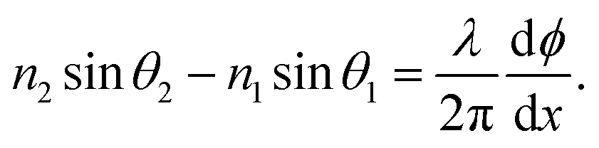 | (3) |
3.4 Attainment of ordered metalens performance by the hyperuniform disordered metalens
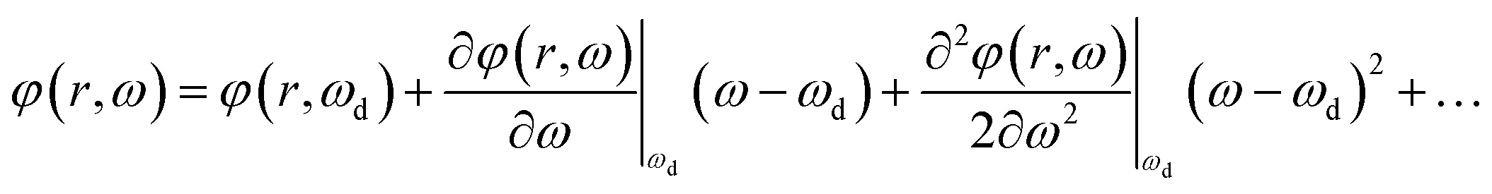
We calculated our proposed metalens structures' performance parameters, such as focal length shift, focusing efficiency, spot size's FWHM, and numerical aperture (NA), for different incident light wavelengths. The optical lensing properties of periodic TiO2 MA distribution are provided in Section S1 of the ESI.†We analyzed the xz-view of electric field distributions for periodic and disordered metalens structures at the wavelengths of 770, 820, 870, 920, and 970 nm, as shown in Fig. 6(a) and (b), respectively. The focal length shift became low when we increased the wavelength of the incident light, which reduced the lens's image quality. However, there is no discernible change in the strength of electric field distributions. Interestingly, our proposed periodic and disordered metalens structures exhibited a linear change in the focal length shift when we changed the wavelength of the incident light, as shown in Fig. 7(a). We calculated the focal length shifts from 2.37 to −8.61 μm and 2.12 to −8.8 μm for periodic and disordered metalens structures, respectively, when we increased the incident light's wavelength from 760 to 970 nm. The focal length shift of periodic and disordered metalens structures due to changing incident optical wavelengths can clearly be seen in Fig. S2 of the ESI.† Here, we considered the increased phase shift beyond the target focal length as a positive focal length shift and the reduced phase shift as a negative one. Meanwhile, the MAs' geometrical characteristics influenced the metalens' optical dispersion, which caused the focal length shift. The Taylor expansion of the wavelength-dependent phase profile elucidates this phenomenon, as described by23
 | (4) |
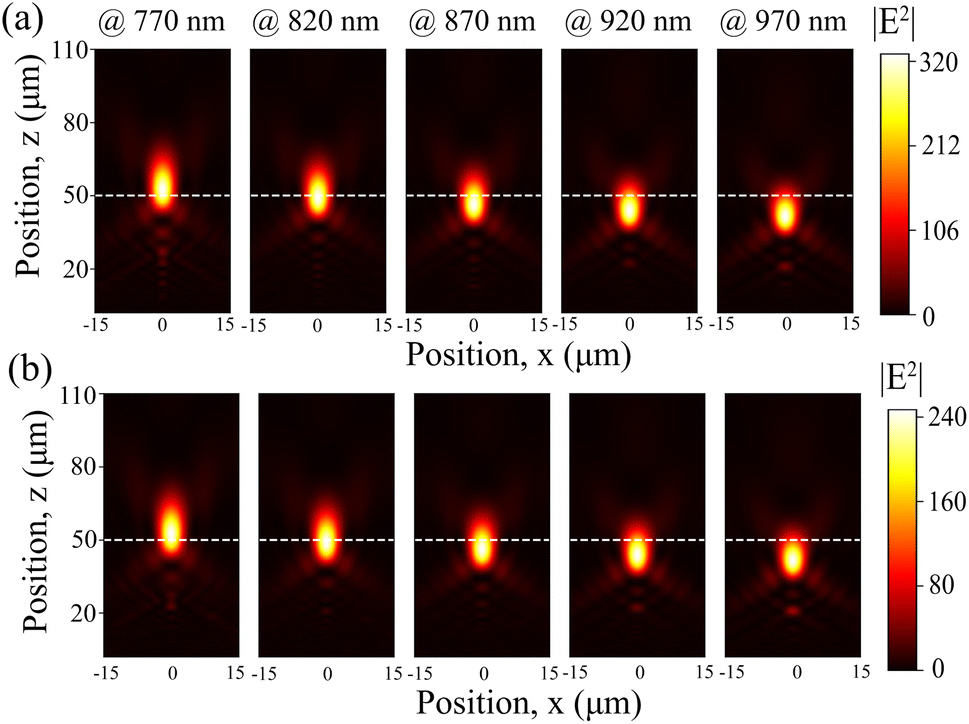 | ||
| Fig. 6 The spatial distributions of electric fields for (a) periodic and (b) disordered metalens structures with varying wavelengths of the incident light. The white dashed lines denote the target focal length of 50 μm. | ||
 | ||
| Fig. 7 (a) The focal length shift, (b) focusing efficiency, (c) FWHM, and (d) NA spectra for periodic and disordered metalens structures. | ||
Here, the right side term regulates the phase shift for a design wavelength (ωd). The first and second derivative terms of eqn (4) provided the group delay and group delay dispersion, resulting in the metalens structures' phase shift. This phenomenon can mitigate adjusting the position of the TiO2 MAs of the metalens structures.
Moreover, we calculated the focusing efficiency of our proposed periodic and disordered metalens structures for varying the wavelength of incident light. Focusing efficiency refers to the proportion of the incident electric field intensity transmitted through the metalens, considering a circular aperture on the focal plane with a diameter three times the FWHM of the focal spot. Our study revealed that hyperuniform distribution can mimic the performance of periodic structures. A similar focusing efficiency was obtained in the wavelength range from 820 to 845 nm, as shown in Fig. 7(b). We achieved the maximum focusing efficiencies of 86.04% and 85.28% for periodic and disordered metalens structures, respectively.
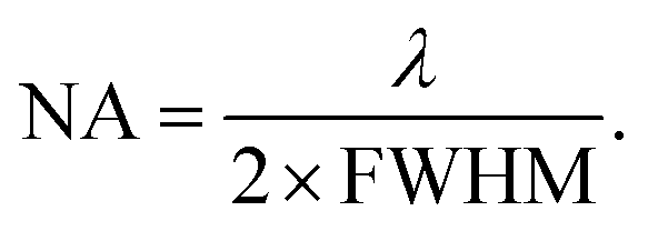
The NA provides information about the size of the metalens structure's focal spot. Therefore, we calculated the NA of our proposed metalens structures by varying the wavelength of the incident light. The NA was calculated using35
 | (5) |
We obtained a constant FWHM of 1.507 and 1.503 μm for periodic and disordered metalenses, respectively, as shown in Fig. 7(c). Afterward, we utilized the FWHM of our proposed metalens structures to calculate the NA. We achieved the NA ranges from 0.2554 to 0.3217 and 0.2561 to 0.3227 for periodic and disordered metalens structures, respectively, as depicted in Fig. 7(d). Here, we considered the Nyquist sampling condition (P < λ/2NA) to maintain the period of MAs, which guaranteed the precise phase shifts of our proposed metalens structures.36
Furthermore, we studied the impact of the minimum distance between two MAs (m) on performance metrics, such as focusing efficiency and the constructed image at the focal length, for the hyperuniform disordered metalens structure. Our proposed hyperuniform disordered metalens structure generated an image at a similar focal length when we varied m, as shown in Fig. 8(a). We obtained a constant focal length of ∼48.65 μm for our proposed disordered structure. We analyzed the focusing efficiency of our proposed disordered structure by varying m. We achieved a maximum focusing efficiency of 84.39% for m = 520 nm, as illustrated in Fig. 8(a). The focusing efficiency was reduced when we increased the m. Therefore, we adopted an m of 520 nm for our study. Fig. 8(b) and (c) illustrate the spatial electric field distribution of the meta-atom at the MA radii of 75 and 150 nm, respectively. We obtained a larger effective index for the MA radius of 150 nm compared to the MA radius of 75 nm. Meanwhile, the MA with a larger radius produced a greater phase shift compared to the MA with a smaller radius. This phenomenon was attributed to the longer effective path for the incident light.
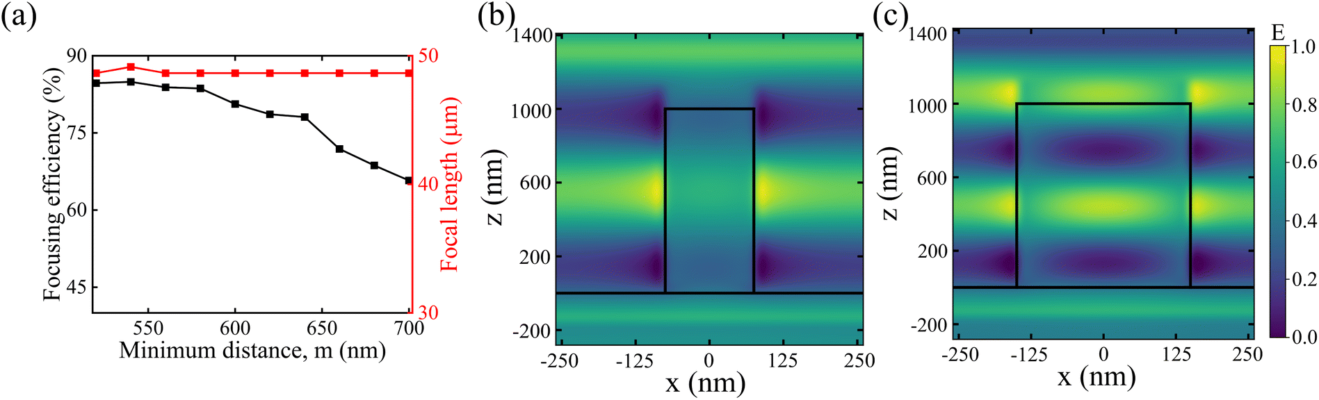 | ||
| Fig. 8 (a) Focusing efficiency and focal length of the disordered metalens structure for varying m. Normalized electric field distribution of the meta-atom for the MA radii of (b) 75 and (c) 150 nm. The bottom and top rectangles represent the SiO2 substrate and TiO2 MA, respectively. | ||
4 Comparative analysis
We conducted a comprehensive comparative performance analysis among our metalens structures and previously reported metalens structures with diverse designs and materials, as listed in Table 1. Conventional and metamaterial-based metalens structures require additional arrangement to couple light efficiently,37,38 which adds complexity to the imaging systems. Li et al.39 and Zhang et al.40 developed GaN nanobar-based metalens structures in the visible wavelength range. They achieved a metalens structure that can provide a narrow FWHM; however, the obtained focusing efficiencies were low. On the other hand, Zhuang et al. reported an ingenious metalens structure positioning TiO2 MAs in a hexagonal pattern.41 Although they obtained a notable NA of 0.95, the focus effectiveness was poor, at around 17.2%. Yang et al. studied a photonic crystal fiber-based near-infrared metalens structure experimentally and numerically.42 However, the performance parameters, such as focal shift, FWHM, and efficiency, were inadequate. Wang et al. proposed a silicon (Si) nanobar-based metalens structure with a maximum focusing efficiency of 50%,43 even though there is a scope to increase the performance parameters. Khorasaninejad et al. and Chen et al. designed TiO2 MA metalens structures in the visible wavelength region.22,23 However, the average efficiency was poor. In contrast, our proposed disordered metalens structure exhibited an outperformed focusing efficiency of 84.39% with a higher NA of 0.2727 compared to previously reported studies. In addition, numerous studies were found by employing ordered or periodic structures; however, there is still a research gap to explore disordered metalens structures, which differentiated our hyperuniform disordered metalens from previously reported periodic metalenses. Moreover, an experimental study obtained a similar result to ours; however, the structure comprised four differently shaped MAs to obtain the desired phase, which requires a complex fabrication technique.8| Structure | Wavelength (nm) | Focal shift (μm) | NA | FWHM (μm) | Maximum focusing efficiency (%) | Ref. |
|---|---|---|---|---|---|---|
| Circular GaN NW dual-layer achromatic | 550 | ∼0 | 0.26 | ∼1.45 | 59 | 39 |
| Polarization tunable rectangular GaN NW | 633 | ∼1.1 | ∼0.257 | ∼1.11 | 63.1 | 40 |
| Hexagonal array of rectangular TiO2 nanopillars | 532 | — | 0.95 | 0.228 | 17.2 | 41 |
| Rectangular air-slotted Au–SiO2 PCF | 1550 | 2 | 0.37 | ∼2.5 | 16.9 | 42 |
| Circularly ordered Si nanopillar | 1065 | — | 0.97 | 5.0 | 50 | 43 |
| Hyperuniform disordered TiO2 MA | 820 | 1.35 | 0.2727 | 1.503 | 84.39 | This work |
5 Conclusion
We proposed a bird's eye-inspired TiO2 MA-based hyperuniform disordered metalens structure employing the FDTD method. The proposed metalens structure generated an image at a focal length by engineering the phase shift of the transmittance via the disordered MA's position. A high focusing efficiency of 84.39% was obtained at a wavelength of 820 nm for disordered metalens structures. Amazingly, a similar focusing efficiency was achieved by the disordered metalens structure compared to the ordered one in a wavelength range from 850 to 890 nm due to the long-range periodic properties of hyperuniform disordered structures, which corroborated the calculated scalar variances of disordered metalens structures. The focal length shifts and NAs of the disordered metalens structure perfectly aligned with the focal length shifts and NAs of the periodic metalens structure in the entire operating region from 770 to 970 nm. We designed the metalens structure for a focal length of 50 μm; however, we obtained the highest intensity of an image at a focal length of 48.65 μm for the disordered metalens structures due to aberration. Additionally, we obtained a constant FWHM of 1.503 μm in the entire operating region for the hyperuniform disordered metalens. The insights gained from our metalens design and performance analysis will be beneficial in developing novel and revolutionary high-resolution imaging, sensing, and spectroscopic technologies.Data availability
Data for this article are available on GitHub at https://github.com/AlphaZero28/metalens-coordinates.git.Author contributions
Ohidul Islam: conceptualization, formal analysis, methodology, visualization, software, investigation, writing – original draft, and writing – review & editing. Dip Sarker: conceptualization, formal analysis, methodology, visualization, software, investigation, writing – original draft, and writing – review & editing. K. B. M. Sharif Mahmood: conceptualization, formal analysis, methodology, visualization, software, and investigation. Joyprokash Debnath: conceptualization and investigation. Ahmed Zubair: supervision, conceptualization, methodology, visualization, project administration, resources, writing – original draft, and writing – review & editing.Conflicts of interest
The authors declare no conflicts of interest.Acknowledgements
The authors appreciate the support of the Bangladesh University of Engineering and Technology (BUET)'s software and computation facility. D. Sarker acknowledges the financial support from BUET through the Postgraduate Fellowship.References
- Z. Liu, H. Lee, Y. Xiong, C. Sun and X. Zhang, Science, 2007, 315, 1686 CrossRef CAS PubMed.
- L. Zhang, S. Chang, X. Chen, Y. Ding, M. T. Rahman, Y. Duan, M. Stephen and X. Ni, Nano Lett., 2023, 23, 51–57 CrossRef CAS PubMed.
- O. Islam, M. H. K. Anik, S. H. Shakib, N. H. Niloy, H. Talukder and S. K. Biswas, Opt Laser. Technol., 2024, 174, 110634 CrossRef.
- M. W. Khalid, J. Ha, M. S. E. Hadri, L. Hsu, S. Hemayat, Y. Xiao, A. Sergienko, E. E. Fullerton and A. Ndao, Adv. Opt. Mater., 2024, 12, 2301599 CrossRef CAS.
- Z. Liu, J. M. Steele, W. Srituravanich, Y. Pikus, C. Sun and X. Zhang, Nano Lett., 2005, 5, 1726–1729 CrossRef CAS PubMed.
- M. Dupré, L. Hsu and B. Kanté, Sci. Rep., 2018, 8, 7162 CrossRef PubMed.
- G. Chen, J. Zhou, S. E. Bopp, J. Zhao and Z. Liu, Opt. Lett., 2022, 47, 4040–4043 CrossRef CAS.
- Y. Wang, Q. Chen, W. Yang, Z. Ji, L. Jin, X. Ma, Q. Song, A. Boltasseva, J. Han, V. M. Shalaev and S. Xiao, Nat. Commun., 2021, 12, 5560 CrossRef CAS PubMed.
- S. Chen, P. Lin, J. Lin and Y.-S. Lin, J. Opt., 2022, 51, 994–1001 CrossRef.
- B. H. Chen, P. C. Wu, V.-C. Su, Y.-C. Lai, C. H. Chu, I. C. Lee, J.-W. Chen, Y. H. Chen, Y.-C. Lan, C.-H. Kuan and D. P. Tsai, Nano Lett., 2017, 17, 6345–6352 CrossRef CAS PubMed.
- D. van Dam, N. J. J. van Hoof, Y. Cui, P. J. van Veldhoven, E. P. A. M. Bakkers, J. Gómez Rivas and J. E. M. Haverkort, ACS Nano, 2016, 10, 11414–11419 CrossRef CAS PubMed.
- Y. Fu, S. Poddar, B. Ren, Y. Xie, Q. Zhang, D. Zhang, B. Cao, Y. Tang, Y. Ding, X. Qiu, L. Shu, J.-F. Liao, D.-B. Kuang and Z. Fan, ACS Nano, 2022, 16, 8388–8398 CrossRef CAS PubMed.
- L. VJ, J. Oh, A. P. Nayak, A. M. Katzenmeyer, K. H. Gilchrist, S. Grego, N. P. Kobayashi, S.-Y. Wang, A. A. Talin, N. K. Dhar and M. S. Islam, IEEE J. Sel. Top. Quantum Electron., 2011, 17, 1002–1032 Search PubMed.
- J. Chen, F. Yu, X. Liu, Y. Bao, R. Chen, Z. Zhao, J. Wang, X. Wang, W. Liu, Y. Shi, C.-W. Qiu, X. Chen, W. Lu and G. Li, Light: Sci. Appl., 2023, 12, 105 CrossRef CAS PubMed.
- K. Ou, F. Yu, G. Li, W. Wang, A. E. Miroshnichenko, L. Huang, P. Wang, T. Li, Z. Li, X. Chen and W. Lu, Sci. Adv., 2020, 6, eabc0711 CrossRef CAS PubMed.
- D. Sarker and A. Zubair, Phys. Chem. Chem. Phys., 2024, 26, 10273–10283 RSC.
- N. Wolchover, A Bird’s-Eye View of Nature's Hidden Order, Quantamagazine, https://www.quantamagazine.org/hyperuniformity-found-in-birds-math-and-physics-20160712/, 2016 Search PubMed.
- M. Florescu, S. Torquato and P. J. Steinhardt, Proc. Natl. Acad. Sci. U. S. A., 2009, 106, 20658–20663 CrossRef CAS PubMed.
- M. M. Milošević, W. Man, G. Nahal, P. J. Steinhardt, S. Torquato, P. M. Chaikin, T. Amoah, B. Yu, R. A. Mullen and M. Florescu, Sci. Rep., 2019, 9, 20338 CrossRef PubMed.
- W. Zhou, Y. Tong, X. Sun and H. K. Tsang, J. Appl. Phys., 2019, 126, 113106 CrossRef.
- N. P. Mitchell, L. M. Nash, D. Hexner, A. M. Turner and W. T. M. Irvine, Nat. Phys., 2018, 14, 380–385 Search PubMed.
- M. Khorasaninejad, W. T. Chen, A. Y. Zhu, J. Oh, R. C. Devlin, C. Roques-Carmes, I. Mishra and F. Capasso, IEEE J. Sel. Top. Quantum Electron., 2017, 23, 43–58 Search PubMed.
- W. T. Chen, A. Y. Zhu, V. Sanjeev, M. Khorasaninejad, Z. Shi, E. Lee and F. Capasso, Nat. Nanotechnol., 2018, 13, 220–226 CrossRef CAS PubMed.
- E. D. Palik, Handbook of Optical Constants of Solids, Academic Press, 1998 Search PubMed.
- R. Bridson, ACM SIGGRAPH 2007 Sketches, New York, USA, 2007, pp. 22–23 Search PubMed.
- O. Islam, D. Sarker, K. B. M. S. Mahmood, J. Debnath, and A. Zubair, Metalens-Coordinates, GitHub, https://github.com/AlphaZero28/metalens-coordinates, 2024 Search PubMed.
- R. Lin, V. Mazzone, N. Alfaraj, J. Liu, X. Li and A. Fratalocchi, Laser Photonics Rev., 2020, 14, 1800296 CrossRef CAS.
- Ansys Lumerical FDTD|Simulation of Photonic Components, https://www.ansys.com/products/optics/fdtd, 2024 Search PubMed.
- S. Torquato, Phys. Rep., 2018, 745, 1–95 CrossRef CAS.
- A. Archetti, R.-J. Lin, N. Restori, F. Kiani, T. V. Tsoulos and G. Tagliabue, Nanophotonics, 2022, 11, 3969–3980 CrossRef CAS PubMed.
- D. Dunbar and G. Humphreys, ACM Trans. Graph., 2006, 25, 503–508 CrossRef.
- H. Nasari, M. Dupré and B. Kanté, Opt. Lett., 2018, 43, 5829–5832 CrossRef PubMed.
- N. Yu, P. Genevet, M. A. Kats, F. Aieta, J.-P. Tetienne, F. Capasso and Z. Gaburro, Science, 2011, 334, 333–337 CrossRef CAS PubMed.
- M. Khorasaninejad, A. Y. Zhu, C. Roques-Carmes, W. T. Chen, J. Oh, I. Mishra, R. C. Devlin and F. Capasso, Nano Lett., 2016, 16, 7229–7234 CrossRef CAS PubMed.
- M. Pan, Y. Fu, M. Zheng, H. Chen, Y. Zang, H. Duan, Q. Li, M. Qiu and Y. Hu, Light: Sci. Appl., 2022, 11, 195 CrossRef CAS PubMed.
- M. K. Chen, Y. Wu, L. Feng, Q. Fan, M. Lu, T. Xu and D. P. Tsai, Adv. Opt. Mater., 2021, 9, 2001414 CrossRef CAS.
- C. Ma, M. A. Escobar and Z. Liu, Phys. Rev. B:Condens. Matter Mater. Phys., 2011, 84, 195142 CrossRef.
- D. Lu and Z. Liu, Nat. Commun., 2012, 3, 1205 CrossRef PubMed.
- M. Li, S. Li, L. K. Chin, Y. Yu, D. P. Tsai and R. Chen, Opt. Express, 2020, 28, 26041–26055 CrossRef PubMed.
- J. Zhang, L. Zhang, K. Huang, Z. Duan and F. Zhao, J. Opt., 2019, 21, 115102 CrossRef CAS.
- Z.-P. Zhuang, R. Chen, Z.-B. Fan, X.-N. Pang and J.-W. Dong, Nanophotonics, 2019, 8, 1279–1289 CrossRef.
- J. Yang, I. Ghimire, P. C. Wu, S. Gurung, C. Arndt, D. P. Tsai and H. W. H. Lee, Nanophotonics, 2019, 8, 443–449 CrossRef CAS.
- Y. Wang, M. Peng, W. Cheng, Z. Peng, H. Cheng, X. Ren, S. Zang, Y. Shuai, H. Liu and J. Wu, et al. , Opt. Express, 2022, 30, 28479–28491 CrossRef CAS PubMed.
Footnotes |
| † Electronic supplementary information (ESI) available. See DOI: https://doi.org/10.1039/d4na00661e |
| ‡ These authors contributed equally to this work. |
| This journal is © The Royal Society of Chemistry 2025 |