 Open Access Article
Creative Commons Attribution 3.0 Unported Licence
Exploring semiconductor potential: novel boron-based Ti3AlC2 and Ti4AlN3 MAX phase composites with tunable band gaps†
Md. Shahinoor
Alam
 *a,
Mohammad Asaduzzaman
Chowdhury
a,
Md. Saiful
Islam
 b,
Md. Moynul
Islam
b,
Md. Abdus
Sabur
b,
Md. Moynul
Islam
b,
Md. Abdus
Sabur
 c and
Md. Masud
Rana
a
aDepartment of Mechanical Engineering, Dhaka University of Engineering and Technology, Gazipur 1707, Bangladesh. E-mail: majshahin4282@gmail.com
bDepartment of Chemistry, Bangladesh Army University of Engineering and Technology, Qadirabad Cantonment, Natore-6431, Bangladesh
cPilot Plant and Process Development Centre, Bangladesh Council of Scientific and Industrial Research (BCSIR), Dhanmondi, Dhaka-1205, Bangladesh
First published on 12th November 2024
Abstract
This research focuses on synthesizing chemically and thermally stable novel in situ Ti4AlN3 and Ti3AlC2 MAX phase reinforced boron-based composites using hot pressed and inert sintering processes, enabling a sizeable and wider bandgap for semiconductor applications. The study found that the MAX phase is formed from 0.2% to 2.9% in fabricated samples with increasing sintering temperatures from 950 °C to 1325 °C. As the sintering temperature increases, the percentage of crystallinity in Ti4AlN3 MAX phase reinforced boron-based composites increases from 69.14% to 89.88%, while in Ti3AlC2 MAX phase reinforced boron-based composites, it increases from 71.02% to 77.86%. And the energy bandgap shows a declining trend from 2.33 eV to 1.78 eV for Ti4AlB2N sample composites and 2.60 eV to 2.40 for Ti4AlB2C sample composites. The UV-vis test for boron-based Ti4AlN3 and Ti3AlC2 MAX phase composites shows an absorbance rate ranging from 0.065 a.u. to 0.63 a.u. and 0.008 to 2.4 a.u. respectively with increasing sintering temperature. Tuning these bandgap variations for Ti4AlN3 and Ti3AlC2 MAX phase reinforced boron-based composites with sintering temperature allows for customization of the material's optical absorption and emission spectra, which is important for semiconductor properties and for electronic and optoelectronic devices.
1. Introduction
MAX phase composites with various metals, metal oxides and metal borides such as zirconium boride (ZrB2), silicon boride (SiB), alumina (Al2O3), boron (B), boron carbide (B4C), boron nitride (BN), and titanium carbide (TiC) have been gaining significant attention in recent years due to their promising properties and semiconductor applications.1,2 A wider and sizeable band gap in such semiconductor materials offers several advantages in electronic and optoelectronic devices. The advantageous properties of these types of semiconductor materials include higher breakdown voltage, lower intrinsic carrier concentration, improved thermal stability, radiation resistance, suitability for optoelectronic applications, high-frequency operation, and reduced sensitivity to temperature variations.3,4 Recently, Avinashi et al. reported that 2-D novel materials and their composites are widely used in many areas such as energy storage, gas sensors, catalysis, and biomedical applications including bio-imaging, drug delivery, therapies, biosensors, tissue engineering, and antibacterial reagents.5 The nanocomposites of ZnO![[thin space (1/6-em)]](https://www.rsc.org/images/entities/char_2009.gif) :
:![[thin space (1/6-em)]](https://www.rsc.org/images/entities/char_2009.gif) SnO2 were synthesized by incorporating SnO2 to ZnO, where the dielectric constant was found to increase.6 Similarly, nano–micro composites of CdO–Al2O3 were fabricated by adding varying amounts of nanostructured CdO to microstructured Al2O3, which also led to enhanced dielectric constants.7 Additionally, Zankat A. et al. studied the frequency- and temperature-dependent electrical properties of ZnO–SnO2 nanocomposites, revealing that these properties are influenced by both temperature and frequency, and attributed the variations to oxygen vacancies, defects, disorder, and structural parameters.8
SnO2 were synthesized by incorporating SnO2 to ZnO, where the dielectric constant was found to increase.6 Similarly, nano–micro composites of CdO–Al2O3 were fabricated by adding varying amounts of nanostructured CdO to microstructured Al2O3, which also led to enhanced dielectric constants.7 Additionally, Zankat A. et al. studied the frequency- and temperature-dependent electrical properties of ZnO–SnO2 nanocomposites, revealing that these properties are influenced by both temperature and frequency, and attributed the variations to oxygen vacancies, defects, disorder, and structural parameters.8
MAX phases are a fascinating class of layered ternary carbides and nitrides. These materials possess a unique combination of metallic and ceramic properties making them attractive for various applications including high-temperature ceramics, wear-resistant coatings, and parts for energy conversion systems.9–11 Their inherent properties like good electrical conductivity, thermal stability, and machinability allow them to be tailored for specific needs.9 Among the MAX phases, titanium aluminum carbide (Ti3AlC2) and titanium aluminum nitride (Ti4AlN3) stand out for their unique combination of mechanical, electrical, and thermal properties.12,13 However, most of the MAX phases including Ti3AlC2 and Ti4AlN3 are unstable and decompose above 1300 °C. Nayebi et al. utilized the Ti3AlC2 phase to lower the sintering temperature and produce TiB2-based composites using spark plasma sintering methods.14 In addition, pure Ti3AlC2 and Ti4AlN3 MAX phases exhibit brittleness, fluctuating coefficients of thermal expansion (CTE),15 and high chemical reactivity, which limit their applications in semiconductor devices. Incorporating boron as amorphous boron (a-B) into these MAX phases further enhances their performance, particularly in semiconductor applications where materials with tailored electrical conductivity, and thermal and chemical stability are crucial.16 Amorphous boron is a promising material with unique properties including high hardness, excellent wear resistance, and interesting electrical and electronic properties.17,18 The potential advantages of a “Ti3AlC2 and Ti4AlN3 MAX phase composite with amorphous boron” over Ti3AlC2 and Ti4AlN3 MAX phases alone in energy storage, optoelectronics, and nanoelectronic devices could be attributed to the unique properties that amorphous boron may bring to the composite material. Due to the enhanced electrical conductivity, tailored band gap, improved thermal conductivity, enhanced mechanical properties, higher specific capacity in energy storage, improved stability and reliability, compatibility with nanofabrication techniques, and versatility in design 2D materials, boron-based Ti3AlC2 and Ti4AlN3 MAX phase composites might be more advantageous in these applications.19
Several studies have explored the development of MAX phase composites to achieve superior properties. For instance, Wozniak et al. fabricated MAX phase/SiC composites demonstrating improved mechanical properties compared to individual phases.20 Nadeem et al. investigated tailoring the electronic properties of Mo2GaC through cationic substitution, highlighting the potential for property modification through composite formation.21 However, synthesizing pure, dense a-B-based MAX phase composites is challenging due to their complex structure and high melting point. Again, a significant challenge lies in developing a synthesis method to achieve a uniform dispersion of boron within the MAX phase composites. Moreover, characterizing the microstructure and properties of such composites to understand the interplay between the phases is crucial. A notable gap exists in the synthesis and characterization of in situ Ti3AlC2 and Ti4AlN3 MAX phase reinforced composites. Moreover, the incorporation of boron and in particular the self-generated boron into these MAX phases and its effects on microstructure and properties relevant to semiconductor applications remain unexplored. Bridging this gap is essential for advancing our understanding of MAX phase composites and unlocking their full potential in semiconductor technology. This research work seeks to address this research gap by synthesizing and characterizing Ti3AlC2 and Ti4AlN3 MAX phase reinforced boron composites, by addressing the self-generated and integrated boron and its impact on material properties, thereby contributing to the advancement of semiconductor applications in nano and optoelectronic devices. With this background, it is expected that (i) chemically and thermally stable Ti3AlC2 and Ti4AlN3 MAX phase reinforced boron composites will be produced using a hot pressed inert sintering process and (ii) semiconductor properties of tunable band gaps and high career mobility will be obtained through the synthesis of MAX phase reinforced amorphous boron composites suitable for electronic and optoelectronic devices as compared to traditional Si, Ge, CdSe, and ZnO-based semiconductor materials. This research is unique in that it is the first attempt to open up new insights for the experimental fabrication of a novel boron carbide-based MAX phase, Ti3AlBC, and boron-nitride-based MAX phase, Ti3AlBN, which has been proven theoretically by the DFT computational approach.16,22 Nonetheless, better knowledge is still required to synthesize boron-based carbide and nitride MAX phases. As we saw throughout the experimental investigation, boron is induced and MAX phases are self-generated in the process rather than the formation of BN and BC MAX phases, and more investigations need to be conducted in this context.
2. Outline of methodology
2.1 Materials
This research is focused on enhancing the semiconductor properties of MAX phase reinforced boron composites. The combination of the Ti3AlC2 or Ti4AIN3 MAX phase with amorphous boron can offer several advantages for semiconductor applications. The unique properties of MAX phases and amorphous boron can complement each other to provide a material with tailored characteristics suitable for semiconductor devices. Incorporating boron as amorphous boron (a-B) into these MAX phases further enhances their performance, particularly in semiconductor applications where materials with tailored electrical conductivity, and thermal and chemical stability are crucial. Amorphous boron is a promising material with unique properties including high hardness, excellent wear resistance, and interesting electrical and electronic properties.17,18 However, synthesizing pure, dense a-B-based MAX phase composites is challenging due to their complex structure and high melting point. Necessary materials and chemicals used in this research work for the synthesis of intended MAX phase composites were in the powder form. These materials were purchased from different sources. Among these, titanium (Ti) powder (Thermo Scientific, −325 mesh, 99.5% purity, CAS # 7440-32-6), aluminum (Al) powder (Thermo Scientific, −100 + 325 mesh, 99.5% purity, CAS # 7429-90-5), and boron nitride (BN) (Sigma-Aldrich, 99% purity, particle size: ≤150 nm, CAS # 10043-11-5) were purchased from USA. Other important chemicals like boron carbide (B4C) (Sigma-Aldrich, 98% purity, particle size: −200 mesh, CAS # 12069-32-8) and acetone (Merk KGaA, K42588114 838 1.00014.1000), utilized for this research work, were purchased from Germany. All other related materials like flash dry silver paint and thinner for flash dry silver paint (SPi supplies, USA, Lot no.: 1180905), and tungsten carbide (WC) powder (Inframat Advanced Materials, 99.9%, Lot: IAM7020WC6, Catalog: 74R-0606) were collected from the local market and utilized without additional purification.2.2 Mass ratio calculation of mixture compounds
This calculation involves balancing the equation, converting substances into moles, using moles rate to estimate the moles of yielded substances in the reaction and converting the moles of required substances to the required units. Molar mass ratios of Ti, Al, BN and B4C for the preparation of working samples are shown in Table 1.| Equation | 4Ti + Al + 2BN → Ti4AlB2N + N |
| Mass ratio | 0.9576![[thin space (1/6-em)]](https://www.rsc.org/images/entities/char_2009.gif) : :![[thin space (1/6-em)]](https://www.rsc.org/images/entities/char_2009.gif) 0.1349 0.1349![[thin space (1/6-em)]](https://www.rsc.org/images/entities/char_2009.gif) : :![[thin space (1/6-em)]](https://www.rsc.org/images/entities/char_2009.gif) 0.2482 0.2482 |
| Equation | 4Ti + Al + B4C → Ti4AlB2C + 2B |
| Mass ratio | 1.9132![[thin space (1/6-em)]](https://www.rsc.org/images/entities/char_2009.gif) : :![[thin space (1/6-em)]](https://www.rsc.org/images/entities/char_2009.gif) 0.2728 0.2728![[thin space (1/6-em)]](https://www.rsc.org/images/entities/char_2009.gif) : :![[thin space (1/6-em)]](https://www.rsc.org/images/entities/char_2009.gif) 0.5523 0.5523 |
2.3 Preparation of working samples (green samples)
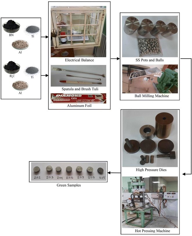
In this research work, the inert sintering process was used after mechanical alloying (ball milling) and hot pressing. A digital electronic balance machine (Model no.: GF12E US-1210, China), spatula (China), brush tuli (China) and aluminum foil (Diamond, China) were utilized for the measuring and weighing purpose of the materials. The pictorial flow diagram of the synthesis process of working samples is illustrated in Fig. 1.Various powder materials (Ti, Al and BN or Ti, Al and B4C) were mixed in a planetary vertical ball milling machine applying a 5![[thin space (1/6-em)]](https://www.rsc.org/images/entities/char_2009.gif) :
:![[thin space (1/6-em)]](https://www.rsc.org/images/entities/char_2009.gif) 1 sample and ball ratio (in weight) at 400 rpm for 4 h for the highest degree of fineness and mixing. A hydraulic hot press (PW 40H, Germany) was used to compress the powder materials at 30 MPa pressure and 380 °C temperature with a high pressure die and mold for obtaining the desired shape of Ti4AlN3 and Ti3AlC2 MAX phase reinforced boron composites (green samples). Initially, 15 MPa cold press was applied at ambient temperature, then the temperature was increased up to 380 °C, the pressure was increased up to 30 MPa gradually and held for 5 minutes to prepare the green samples. A total of 2 types of ten samples, 5 samples of Ti4AlB2N and 5 samples of Ti4AlB2C, were prepared and sintered at different temperatures to be used in experiments as shown in Table 2.
1 sample and ball ratio (in weight) at 400 rpm for 4 h for the highest degree of fineness and mixing. A hydraulic hot press (PW 40H, Germany) was used to compress the powder materials at 30 MPa pressure and 380 °C temperature with a high pressure die and mold for obtaining the desired shape of Ti4AlN3 and Ti3AlC2 MAX phase reinforced boron composites (green samples). Initially, 15 MPa cold press was applied at ambient temperature, then the temperature was increased up to 380 °C, the pressure was increased up to 30 MPa gradually and held for 5 minutes to prepare the green samples. A total of 2 types of ten samples, 5 samples of Ti4AlB2N and 5 samples of Ti4AlB2C, were prepared and sintered at different temperatures to be used in experiments as shown in Table 2.
| Sample compound | Samples' names and their sintering temperatures | ||||
|---|---|---|---|---|---|
| 950 °C | 1050 °C | 1150 °C | 1250 °C | 1325 °C | |
| Ti4AlB2N | Sample 306C | Sample 206B | Sample 306A | Sample 306B | Sample 206A |
| Ti4AlB2C | Sample 309C | Sample 209B | Sample 309A | Sample 309B | Sample 209A |
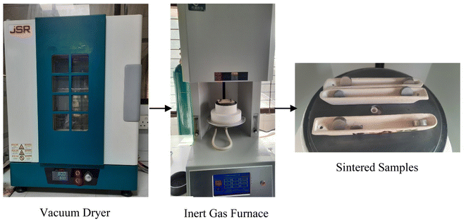
The green samples were inserted into a Vacuum Dryer (JSVO-30T, Korea) for 24 hours at 80 °C before sintering. The dried samples were taken into an inert gas furnace (Dental elevator, Model: CY-1400-cocr, China) and sintered at 950 °C, 1050 °C, 1150 °C, 1250 °C and 1325 °C temperatures in a porcelain vessel with a heating and cooling rate of 5 °C min−1 with 2 hours holding time for each sample. The inert environment in the furnace was maintained using Ar gas with a mass flow rate of 4–5 L min−1. The overall drying and sintering process of the green samples is shown in Fig. 2.
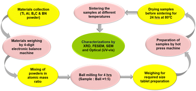
After cooling and necessary preparations, the sample composites were used for further testing and analysis. The schematic flow diagram of the overall synthesis process and experimental techniques is shown in Fig. 3.
Molar mass ratios of powder compositions, sintering method, sintering temperature, sintering time, inert environment, retarding of oxide formation (drying), and also diffusion were taken into account in this study. Their effects on structural and phase formation were investigated.
Characteristics and phase formation were analyzed by using different characterization techniques as mentioned below.
3. Characterization techniques
3.1 XRD
A Malvern Panalytical instrument, Netherlands, Model: 9430 060 03000 was used for XRD analysis. Data were accumulated by a using data viewer with “ORIGIN” and then “HIGH SCORE” software. Measurement conditions of scan range: 20° to 89°, configuration: flat sample stage, goniometer: theta/theta, minimum step size 2theta: 0.0001, minimum step size omega: 0.0001, sample stage: stage for flat samples/holders, diffractometer system: EMPYREAN, anode material: Cu, K-α1 wavelength: 1.540598 Å, divergence slit type: fixed and slit size [°]: 0.76, generator voltage: 45 kV, tube current: 40 mA, h k l: 0 0 0, scan axis: Gonio, scan step size [°2θ]: 0.0262606, number of points: 3046, scan type: continuous, time per step (s): 46.665 were considered. The MAX phase composite samples were first ground into fine powders using a mortar and pestle to confirm uniform particle size distribution. The powder was then placed into a sample holder. Finally, the sample was carefully aligned in the XRD instrument to ensure accurate diffraction measurements across the desired range of 2θ angles.3.2 FESEM
A field emission scanning electron microscopy (FESEM) instrument of Model: JSM-7610F JEOL, Japan was used to get topographical data on the surface of fabricated sample composites using PC-SEM, JEOL software. The operating conditions of volt: 15 kV, probe current: 1 nA, PHA mode: T3, counting rate: 77 cps, energy range: 0–20 keV, method: ZAF and fitting coefficient: 0.6414 were applied to get high magnification images of the samples for necessary analysis. For the FESEM tests, sintered tablet samples were cleaned with an isopropanol to remove any debris and gold coated by an agar sputter coater, and then the sample was placed in the test chamber at an appropriate accelerating voltage to capture high-resolution images of the microstructure.3.3 SEM
A scanning electron microscopy (SEM) machine of TESCAN, Czech Republic, Model: VEGA COMPACT LMH 123-0141 was used for SEM analysis of targeted sample surfaces. The operating conditions of mode: continual, dead time: 2%, landing energy: 15 keV, beam current: 3 nA and coating element: gold were applied to conduct this test.3.4 Optical (UV-vis)
A UV-vis spectrophotometer of Model: A12536103565 CD, SHIMADZU, UV-1900i, China was used for optical characterization of synthesized MAX phase composite samples. The machine was calibrated first and then the sample holder and standard vial were set. The linear and non-linear absorbance of 0–1 Au was fixed. The wavelength (λ) range 190–1100 nm was taken and the sample was considered as the direct material where n = ½ was set.4. Results and discussion
4.1 XRD analysis
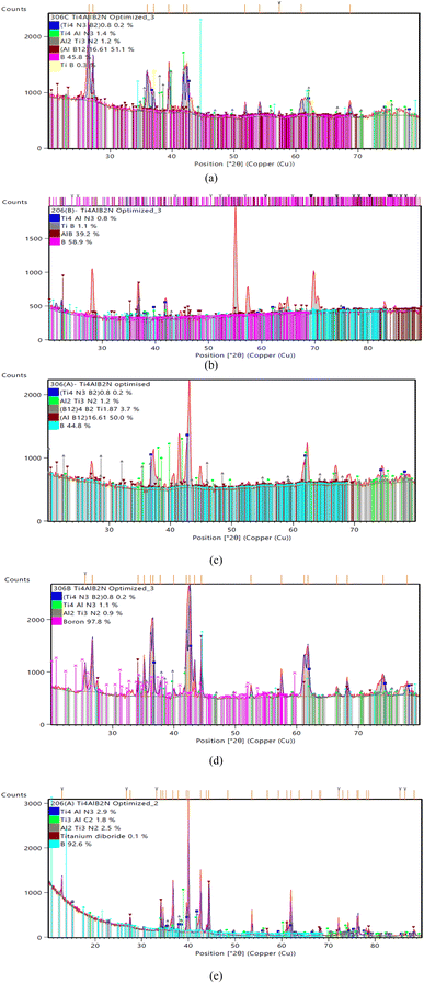
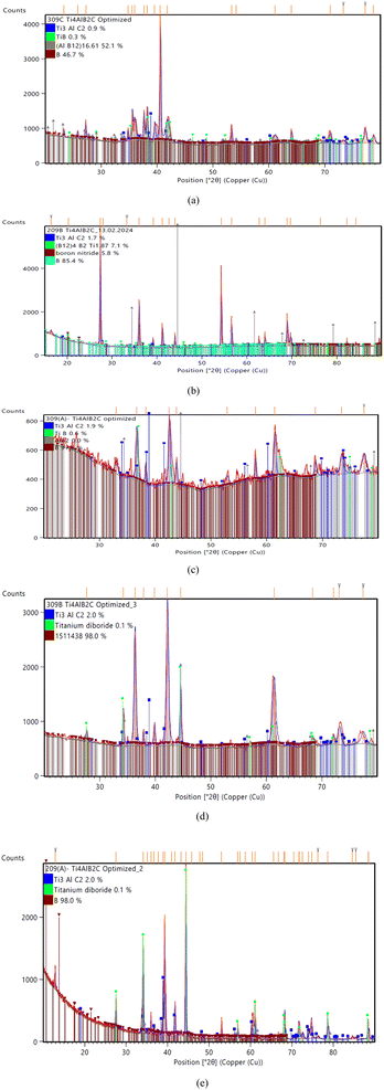
The specimen under investigation was in a highly pulverized form, having undergone extensive mixing to ensure uniformity. The sintered samples as prepared were scanned through the 2θ angle range to capture all lattice scattering orientations caused by random powder material orientations.23,24 In order to examine the development of Ti3AlC2 and Ti4AlN3 MAX phases and amorphous boron and determine the interplanar distance in green samples, XRD experiments were conducted. The peak analyzing the view of main graphics of all XRD spectra shows the percentage of various compounds in fabricated composites that were sintered at different temperatures, which are depicted in Fig. 4 and 5 and projected in Table 3. From Table 3, it is found that in both the cases the MAX phase is formed as shown in Fig. 6(a) and (b), which is usually increased slightly from 0.2% to 2.9% with increasing temperatures from 950 °C to 1325 °C in the case of Ti4AlB2N samples. With increasing temperature, it is also found that the percentage of boron is increased from 45.8% to 97.8%. Again, in the case of Ti4AlB2C samples, the MAX phase is found to increase from 0.9% to 2.0% and the percentage of boron is found to increase from 46.7% to 98.0% under similar conditions. With increasing temperature and particularly the onset of over-sintering it is also observed that additional phases or intergranular reactions occur, reintroducing defects and potentially forming secondary phases in both the cases for all the fabricated sample composites.| Sample compound | Compositions of samples sintered at different temperatures | Remarks | ||||
|---|---|---|---|---|---|---|
| Ti4AlB2N | Sample 306C (950 °C) | Sample 206B (1050 °C) | Sample 306A (1150 °C) | Sample 306B (1250 °C) | Sample 206A (1325 °C) | MAX phase formation increases with the increase of sintering temperature. Amorphous B is dispersed uniformly |
| Ti4AlN3 = 1.4%, (Ti4N3B2) = 0.2%, Al2Ti3N2 = 1.2%, (AlB12) = 51.1%, B = 45.8%, TiB = 0.3% | Ti4AlN3 = 0.8%, TiB = 1.1%, AlB = 39.2%, B = 58.9% | Ti4AlN3 = 0% (Ti4N3B2) = 0.2%, Al2Ti3N2 = 1.2% (B12)4B2Ti = 3.7%, (AlB12) = 50.0%, B = 44.8% | Ti4 AlN3 = 1.1% (Ti4N3B2) = 0.2%, Al2Ti3N2 = 0.9%, B = 97.8% | Ti4AlN3 = 2.9%, Ti3AlC2 = 1.8%, Al2Ti3N2 = 2.5%, TiB2 = 0.1%, B = 92.6% | ||
| Ti4AlB2C | Sample 306C (950 °C) | Sample 206B (1050 °C) | Sample 306A (1150 °C) | Sample 306B (1250 °C) | Sample 206A (1325 °C) | MAX phase formation increases with the increase of sintering temperature. Amorphous B is dispersed more uniformly |
| Ti3AlC2 = 0.9%, TiB = 0.3%, (AlB12) = 52.1%, B = 46.7% | Ti3AlC2 = 1.7%, (B12)4B2Ti = 7.1%, BN = 5.8%, B = 85.4% | Ti3AlC2 = 1.9%, TiB = 0.6%, AlB2 = 0.0%, B = 97.5% | Ti3AlC2 = 2.0%, TiB2 = 0.1%, B = 98.0% | Ti3AlC2 = 2.0%, TiB2 = 0.1%, B = 98.0% | ||
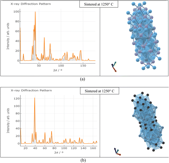 | ||
| Fig. 6 X-ray diffraction pattern and crystal structure (P63/mmc) of (a) Ti4AlN3 and (b) Ti3AlC2 MAX phases. | ||
 | (1) |
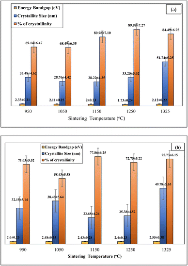
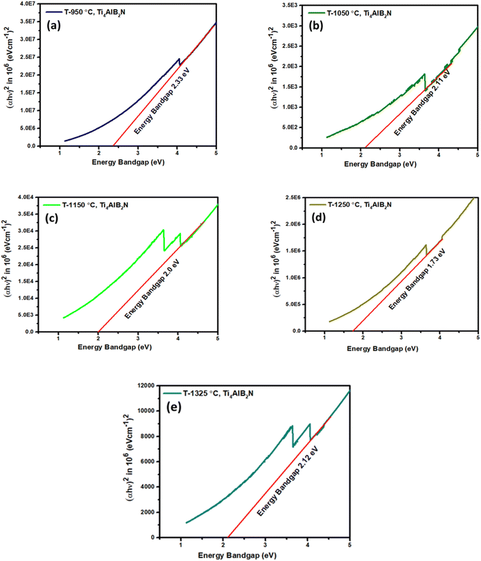
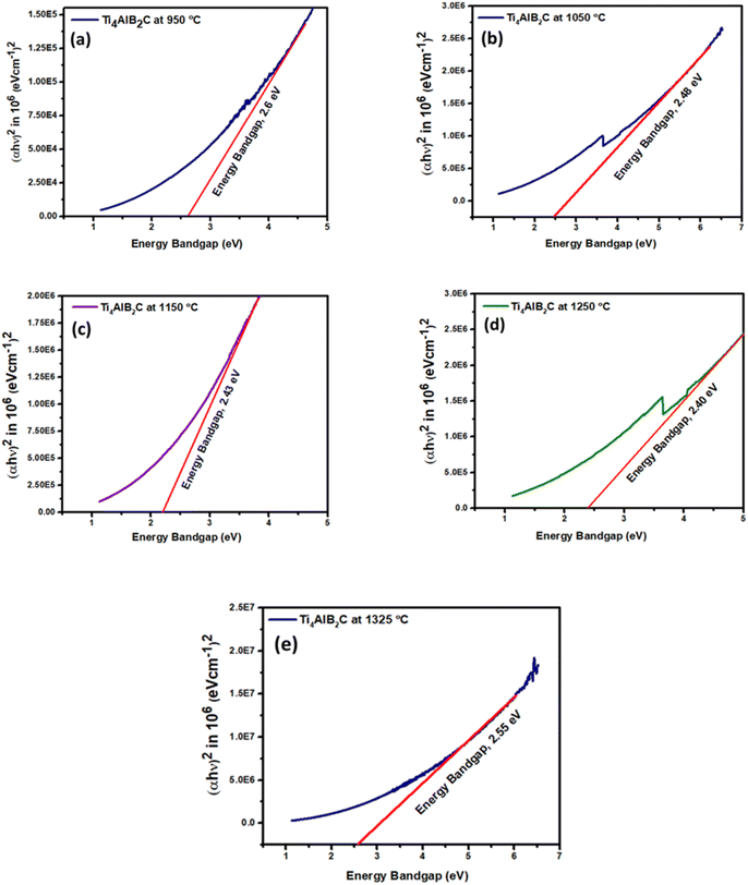
From Table 4 and Fig. 7, it is observed that the percentage of crystallinity increases for both the composites with increasing sintering temperature. In the case of Ti4AlN3 MAX phase reinforced boron-based composites, the percentage of crystallinity increases from 69.14% to 89.88% and in the case of Ti3AlC2 MAX phase reinforced boron based composites the percentage of crystallinity increases from 71.02% to 77.86%. And it is observed that when the percentage of crystallinity increases, the energy bandgap shows a declining trend from 2.33 eV to 1.78 eV for Ti4AlB2N sample composites and 2.60 eV to 2.40 for Ti4Al B2C sample composites. Higher crystallinity generally enhances the mechanical, thermal, and optical properties of a material. In highly crystalline materials, atoms are arranged in a regular, repeating pattern, which facilitates efficient transmission of electrons and phonons, leading to better electrical conductivity and thermal conductivity. Additionally, high crystallinity often results in increased strength and hardness because the orderly atomic structure can better resist deformation. Conversely, materials with low crystallinity, such as amorphous materials, typically exhibit lower mechanical strength and thermal conductivity but may have superior flexibility and impact resistance.26
| Sample name | Sintering temperature (°C) | Energy bandgap (eV) | % of crystallinity | Average crystallite size, D (nm) | Average dislocation density | Average microstrain, (ε) δ |
|---|---|---|---|---|---|---|
| Ti4AlB2N | 950 | 2.33 | 69.14479301 | 33.4801158 | 0.000892126 | 0.174 |
| 1050 | 2.11 | 68.49341763 | 28.75657405 | 0.001209277 | 0.3706 | |
| 1150 | 2.00 | 80.98498124 | 28.22378443 | 0.001255364 | 0.1905 | |
| 1250 | 1.73 | 89.87724096 | 33.25336288 | 0.000904334 | 0.1809 | |
| 1325 | 2.12 | 84.49385884 | 51.74103091 | 0.000373534 | 0.13325 | |
| Ti4AlB2C | 950 | 2.60 | 71.02942065 | 32.14693379 | 0.000967656 | 0.1954 |
| 1050 | 2.48 | 58.43002545 | 38.47868919 | 0.000675398 | 0.214 | |
| 1150 | 2.43 | 77.85832197 | 23.68582858 | 0.001782472 | 0.2405 | |
| 1250 | 2.40 | 72.7525578 | 25.37922385 | 0.001552542 | 0.2148 | |
| 1325 | 2.55 | 75.72842043 | 49.78197252 | 0.000403511 | 0.1309 |
 | (2) |
From the tabulated results in Table 4 and Fig. 7, it is observed that there is a small variation noticed in the crystallite size of fabricated samples with increasing temperature from 950 °C to 1250 °C and an optimal crystallite size is found in this range but after 1250 °C, the variation in crystallite size was observed to be more. Smaller crystallites, or nanocrystallites, can enhance certain properties, such as hardness and strength, through the Hall–Petch effect, which states that smaller grains inhibit dislocation motion, thereby strengthening the material. However, very small grains can also lead to an increased grain boundary area, which can act as sites for corrosion and reduce the material's overall ductility. Larger crystallites usually mean fewer grain boundaries, which can enhance the material's ductility and electrical conductivity but may reduce hardness and strength. The optimal crystallite size is often a balance between these competing effects and depends on the intended application of the material.29
| Dislocation density, δ = 1/D2 | (3) |
From the calculated results as shown in Table 4 and projected in Fig. 7, it is found that there is a declining trend in average dislocation density from 0.0012 to 0.0003 with increasing sintering temperature in the case of Ti4AlN3 MAX phase reinforced boron-based composites, and in the case of Ti3AlC2 MAX phase reinforced boron-based composites it is observed to be from 0.0009 to 0.0004. In both the cases the average dislocation density is found to be very low and well controlled. Low dislocation density is generally desired for applications requiring high ductility and toughness, as it reduces internal stresses and potential sites for crack initiation. High dislocation density typically results from plastic deformation or rapid solidification processes and can significantly impact a material's mechanical properties. While dislocations can strengthen a material by impeding the movement of other dislocations (work hardening), excessive dislocations can also act as stress concentrators, leading to increased brittleness and a higher likelihood of fracture. In materials where high strength is crucial, controlling dislocation density is essential, as it directly influences the yield strength and fatigue resistance.31,32
Microstrain, ε = β/4![[thin space (1/6-em)]](https://www.rsc.org/images/entities/char_2009.gif) tan tan![[thin space (1/6-em)]](https://www.rsc.org/images/entities/char_2009.gif) θ θ | (4) |
From the calculation it is found that the average microstrain is reduced from 0.370 to 0.133 in the case of Ti4AlB2N samples and 0.195 to 0.130 in the case of Ti4AlB2C samples. Managing microstrain is crucial in materials design, especially for high-performance applications, as it ensures structural integrity and reliability.34 High microstrain often indicates a high level of internal stress, which can lead to premature failure under mechanical loading. It can also impact the material's mechanical properties, including its yield strength and fatigue life. However, microstrain can be reduced through processes like annealing, which can enhance ductility and toughness by relieving internal stresses.
4.2 FESEM analysis
Field Emission Scanning Electron Microscopy (FESEM) provides detailed images of the surface morphology revealing characteristic layered structures. These layered structures are often indicative of the presence of MAX phases. While FESEM provides surface and microstructural details confirming MAX phase formation, it often requires a correlation with XRD, which gives definitive information about the crystal structure.35–38 By correlating the high-resolution images and elemental composition data from FESEM (as shown in Fig. 8 and 9) with the crystal structure information from XRD (as shown in Fig. 6 and Table 4), the formation of MAX phases can be robustly confirmed. The detailed surface and compositional analyses from FESEM support and verify the structural findings from XRD results as shown in Table 4, providing a comprehensive understanding of the material's properties and confirming the successful synthesis of the desired MAX phase composites.4.3 SEM analysis
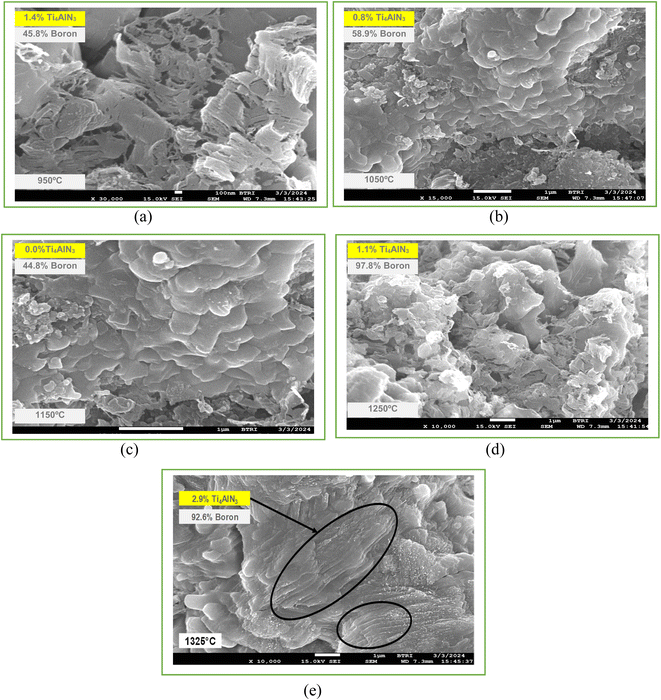
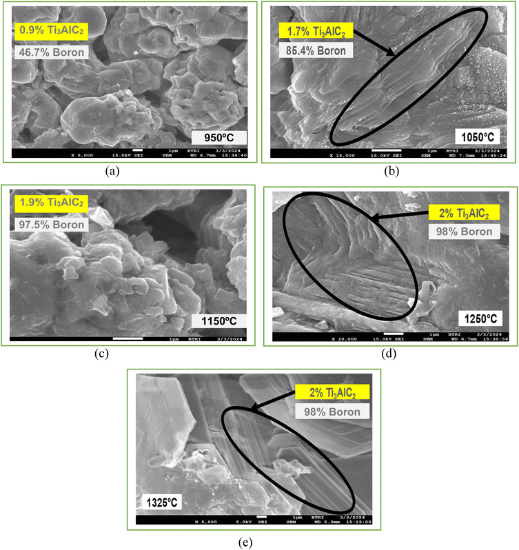
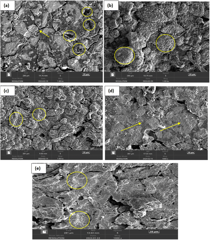
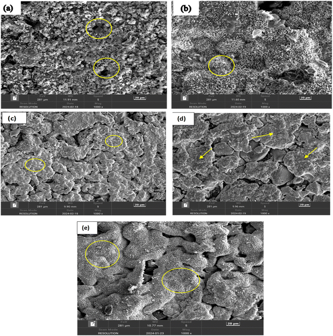
In order to investigate the surface morphology of self-generated Ti4AlN3 and Ti3AlC2 MAX phase composites with amorphous boron, the SEM test was conducted. The effect of sintering temperature on the microstructure of MAX-phase composites was observed through this investigation. Fig. 10(a–e) and 11(a–e) display the SEM images of various MAX-phase composites sintered at different temperatures (950 °C, 1050 °C, 1150 °C, 1250 °C and 1325 °C). At 950 °C, the composite shows incomplete sintering with noticeable porosity and loosely bonded grains, indicating limited diffusion and phase formation, as seen for both Ti4AlB2N and Ti3AlB2C composites in Fig. 10 (a) and 11(a). At this temperature, the SEM images also show intergranular cracks and voids throughout the surfaces of MAX phase composites. As the temperature increases to 1050 °C, the images reveal improved grain bonding and reduced porosity, suggesting enhanced diffusion and initial densification (Fig. 10(b) and 11b). The grains become very large and the boundaries become less distinct, indicating that the material has undergone significant reorganization, which can enhance its phase stability and impact its properties.39For sintering temperature at 1150 °C, the microstructure exhibits more pronounced grain growth and a denser packing, with fewer voids and better-defined grain boundaries, indicating significant phase formation and consolidation. Moreover, the agglomerates of chemical compositions are also observed in Fig. 10(c) and 11(c) at this temperature. Fig. 10(d) and 11(d) depict a more compact surface structure for both Ti4AlB2N and Ti3AlB2C composites sintered at a temperature of 1250 °C. This indicates the successful formation of Ti4AlN3 and Ti3AlC2 MAX phases with amorphous boron, as observed in other studies.40–43
Finally, at 1325 °C, the SEM images display a highly dense and well-sintered composite, with minimal porosity and large well-bonded grains. At this temperature, the composite surfaces also showed some layers of Ti4AlN3 MAX phase (Fig. 10(e)) and Ti3AlC2 MAX phase (Fig. 11(e)). However, amorphous boron was more visible on Ti3AlC2 MAX phase composite surfaces than that of the Ti4AlN3 MAX phase. The amorphous boron regions become more integrated within the MAX matrix, contributing to a more uniform and homogeneous microstructure.44–49 These images collectively demonstrate the critical role of sintering temperature in influencing the densification, grain growth, and overall microstructural integrity of the MAX phase composites. Furthermore, the microstructural changes with temperature directly influence the composite's mechanical strength, toughness, semiconductor properties, and thermal stability which are important for potential applications. The amorphous boron is visible at dispersed regions within the matrix, often appearing more uniform and less structured due to its non-crystalline nature. As previously stated, all of these lead to the in situ formation of amorphous boron with dispersed Ti4AlN3 and Ti3AlC2 MAX phases in the composites.
4.4 Ultraviolet-visible (UV-vis) spectroscopy analysis
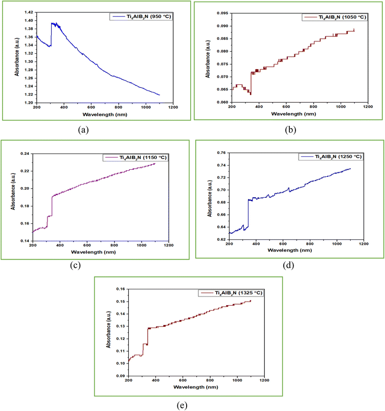
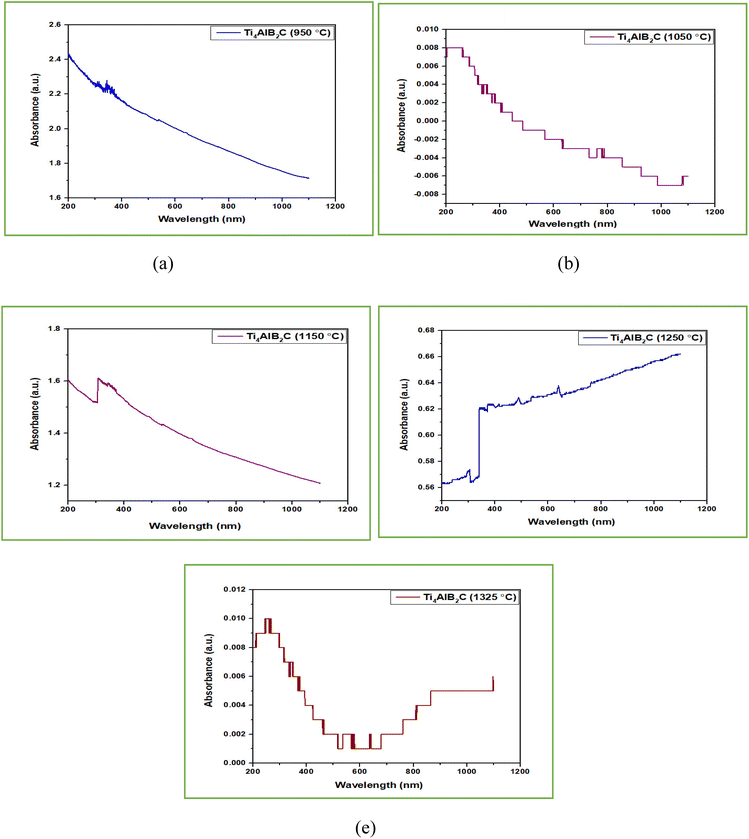
UV-vis spectroscopy refers to absorption spectroscopy or reflectance spectroscopy in part of the ultraviolet and the full, adjacent visible regions of the electromagnetic spectrum.50 UV-vis tests were conducted to understand the optical characteristics of different Ti4AlB2N and Ti4AlB2C samples. The UV spectra of all sintered samples are shown in Fig. 12 and 13.For optoelectronic devices such as photodetectors, solar cells, and LEDs, a balanced absorbance rate ensures that the material is not overly opaque, allowing for efficient light transmission and interaction with the active regions. This balance is crucial for optimizing the device's performance by enabling effective light absorption where needed without excessive thermal losses. An absorbance rate in this range helps in preventing the formation of UV-induced defects by not allowing too much UV energy to penetrate and interact with the semiconductor material. This helps in maintaining the purity and performance of the semiconductor, avoiding issues such as increased electron–hole recombination rates that can reduce device efficiency.53,54
High absorbance rates are generally detrimental to semiconductor applications due to the associated risks of material degradation, thermal instability, reduced optoelectronic performance, and increased susceptibility to contamination effects. Ensuring low to moderate UV absorbance (from 0.1 to 1.6 a.u.) helps maintain the structural and electronic integrity of semiconductor materials, thereby enhancing device reliability and efficiency. An absorbance rate in the range of 0.05 to 0.65 a.u. for Ti4AlN3 MAX phase reinforced boron based composites is considered good for semiconductor properties because it provides a balance between UV protection and material stability. This range helps in maintaining the structural and electronic integrity of the semiconductor, ensures thermal stability, and optimizes the performance of optoelectronic devices. It minimizes the risks associated with high absorbance, such as material degradation and thermal stress, while allowing for sufficient UV transparency to prevent significant energy loss.55,56
Semiconductor devices often rely on the efficient absorption of UV light to generate electrical signals or perform specific functions. A low absorbance rate within this range ensures that the semiconductor material efficiently absorbs UV light, leading to enhanced device performance in terms of sensitivity, response time, and signal-to-noise ratio. The specified range (0.008 to 0.65 a.u.) suggests that the material's absorbance is well-controlled within the desired UV spectral range. This is crucial for semiconductor applications that operate within specific UV wavelengths, ensuring that the material's optical properties align with the requirements of the application. Semiconductor fabrication processes often involve exposure to UV light for various steps such as patterning, doping, or annealing. A boron-based Ti3AlC2 MAX phase composite with a low absorbance rate within this range is compatible with such processes, minimizing unwanted absorption or interference during manufacturing. Consistent and low absorbance within the specified range indicates good material quality and stability, which are essential for the long-term reliability of semiconductor devices. It suggests that the material's optical properties will remain consistent over time, minimizing performance degradation or drift.58
Semiconductors are commonly used in photodetectors, where they convert incident light (UV, in this case) into electrical signals. Low absorbance means more UV light can penetrate the material, increasing the number of photons available for detection. This enhances the photodetection efficiency of the semiconductor device. In conclusion, a boron-based Ti3AlC2 MAX phase composite with a low absorbance rate falling within the range of 0.008 to 0.65 a.u. in a UV test is highly desirable for semiconductor applications. It offers optical transparency, supports device performance, aligns with specific spectral requirements, ensures process compatibility, and enhances the reliability and stability of semiconductor devices.51
| (αhv)n = A(hv − Eg) | (5) |
| Sample compound | Band gap, MAX phase and boron% of prepared samples at different sintering temperatures | |||||
|---|---|---|---|---|---|---|
| Sample name | Sample 306C (950 °C) | Sample 206B (1050 °C) | Sample 306A (1150 °C) | Sample 306B (1250 °C) | Sample 206A (1325 °C) | |
| Ti4AlB2N | Bandgap (eV) | 2.33 | 2.11 | 2.00 | 1.73 | 2.12 |
| MAX phase (Ti4AlN3)% | 1.4 | 0.8 | 0 | 1.1 | 2.9 | |
| Sample compound | Band gap, MAX phase and boron% of prepared samples at different sintering temperatures | |||||
|---|---|---|---|---|---|---|
| Sample name | Sample 309C (950 °C) | Sample 209B (1050 °C) | Sample 309A (1150 °C) | Sample 309B (1250 °C) | Sample 209A (1325 °C) | |
| Ti4AlB2C | Bandgap (eV) | 2.60 | 2.48 | 2.43 | 2.40 | 2.55 |
| MAX phase (Ti3AlC2)% | 0.9 | 1.7 | 1.9 | 2.0 | 2.0 | |
| Boron% | 47.7 | 85.4 | 97.5 | 98 | 98 | |
4.4.3.1 Bandgap of Ti4AlN3 MAX phase reinforced boron-based composites (Ti4AlB2N). The variation in the bandgap of Ti4AlN3 MAX phase reinforced boron-based composites (Ti4AlB2N) with sintering temperature reveals important insights into the material's structural and electronic properties. At a lower sintering temperature, such as 950 °C, the material exhibits a relatively high bandgap of 2.33 eV due to smaller grain sizes and a higher number of defects and grain boundaries. These imperfections create localized states within the bandgap. As the sintering temperature increases to 1050 °C and 1150 °C, the bandgap decreases to 2.11 eV and 2.00 eV, respectively. This reduction is attributed to grain growth and enhanced crystallinity, which diminish the number of defect states. At an optimal sintering temperature of 1250 °C, the material achieves its lowest bandgap of 1.73 eV. This temperature promotes the highest degree of structural order and crystallinity, significantly reducing defects and grain boundaries, and thus minimizing localized electronic states within the bandgap. However, further increasing the temperature to 1325 °C leads to a rise in the bandgap to 2.12 eV. This increase suggests the onset of over-sintering, where additional phases or intergranular reactions occur, reintroducing defects and potentially forming secondary phases, which adversely affect the band structure.
The changes in bandgaps with sintering temperature have substantial implications for semiconductor applications. Materials with a lower bandgap, such as those sintered at 1250 °C, are desirable for electronic and optoelectronic devices due to their efficient charge carrier movement. However, the increase in bandgaps at higher temperatures indicates potential issues with thermal and phase stability, which could limit the material's performance in high-temperature environments.64,65 These factors highlight the delicate balance required in the sintering process to achieve desired electronic properties for semiconductor applications. Appropriate control of the sintering temperature is essential to optimize the grain size, reduce defects, and prevent unwanted phase transformations, thereby tailoring the bandgap for specific electronic and optoelectronic uses.66,67
4.4.3.2 Bandgap of Ti3AlC2 MAX phase reinforced boron-based composites (Ti4AlB2C). The variation in bandgap values for Ti3AlC2 MAX phase reinforced boron-based composites (Ti4AlB2C) with different sintering temperatures can be explained by examining the material's structural and electronic changes during the sintering process. At a lower sintering temperature of 950 °C, the material has a high concentration of defects and smaller grain sizes. Defects such as grain boundaries, vacancies, and interstitials create localized states within the bandgap, leading to a higher bandgap value of 2.60 eV. Additionally, incomplete sintering may result in less optimal crystallinity, contributing to the wider bandgap. With an increase in temperature at 1050 °C, 1150 °C and 1250 °C, the grains start to grow, reducing the number of grain boundaries and defects. This reduction in defect states causes the bandgap to decrease slightly at 2.48 eV, 2.43 eV and 2.40 eV respectively. The balance between reduced defect density and the potential for new defect formation can cause minor fluctuations in the bandgap. The material reaches an optimal sintering state at a temperature of 1250 °C, where the crystallinity is highest and the defect concentration is minimized. Larger grain sizes and fewer grain boundaries contribute to fewer localized electronic states within the bandgap, resulting in the lowest bandgap value of 2.40 eV. This indicates an optimal balance of structural order and electronic properties. Further increasing the temperature at 1325 °C leads to over-sintering, where new defects or secondary phases may form. These new defects or intergranular reactions can introduce localized states within the bandgap, causing an increase in the bandgap of 2.55 eV again. The formation of these secondary phases or defects disrupts the optimal electronic structure achieved at lower temperatures.68
The growth of grains and reduction of grain boundaries with increasing temperature initially reduce defect states, lowering the bandgap. However, excessive grain growth or the formation of secondary phases at higher temperatures can reintroduce defects. The concentration of defects such as vacancies, interstitials, and grain boundaries directly affects the bandgap. An optimal sintering temperature minimizes these defects, resulting in the lowest bandgap, while too high or too low sintering temperatures increase defects. At very high temperatures, phase transformations or secondary phase formations can alter the electronic structure, leading to increased bandgap values.69
The sintering temperature has a significant impact on the bandgap of Ti3AlC2 MAX phase reinforced boron-based composites. An optimal sintering temperature around 1250 °C minimizes defects and achieves the lowest bandgap, making the material suitable for high-efficiency semiconductor applications. However, temperatures above this optimal point can introduce new defects or secondary phases, increasing the bandgap and potentially limiting the material's utility in certain applications. Controlling the sintering process is essential to optimize the material's properties for specific electronic and optoelectronic applications.
4.4.3.3 Impact of resultant bandgaps on semiconductor applications. The sintering temperature-dependent bandgap variations as shown in Table 5 for Ti4AlN3 and Ti3AlC2 MAX phase reinforced boron-based composites reveal distinct behaviors that affect their suitability for semiconductor applications. For Ti4AlN3 composites, the bandgap decreases from 2.33 eV at 950 °C to a minimum of 1.73 eV at 1250 °C before increasing to 2.12 eV at 1325 °C. This trend suggests that up to 1250 °C, the material's crystallinity improves, and defects decrease, leading to a lower bandgap. The increase at 1325 °C indicates over-sintering, introducing new defects or secondary phases. In contrast, Ti3AlC2 composites show a bandgap decrease from 2.60 eV at 950 °C to 2.40 eV at 1250 °C, and then rising to 2.55 eV at 1325 °C. The initial decrease reflects grain growth and reduced defects. The optimal bandgap of 2.40 eV at 1250 °C indicates good sintering conditions, with the increase at 1325 °C again pointing to over-sintering effects.
Materials with lower bandgap values, such as those sintered at 1250 °C, are preferable for applications that require efficient charge carrier movement, such as transistors, solar cells, and light-emitting diodes (LEDs). The minimized defects and optimal electronic properties at this temperature make the material suitable for high-performance applications.70,71 The increase in bandgaps at higher temperatures (1325 °C) suggests potential issues with thermal and phase stability. Devices operating at high temperatures may experience changes in electronic properties, affecting performance.72,73 The ability to tune the bandgap with sintering temperature allows for customization of the material's optical absorption and emission spectra. This is important for optoelectronic applications, where specific bandgap values are required for different functionalities.74
Ti4AlN3 MAX phase reinforced boron based composites are more suitable for semiconductor applications requiring lower bandgaps, such as optoelectronic devices, due to their minimum bandgap of 1.73 eV at 1250 °C, indicating high efficiency and good crystallinity. On the other hand, Ti3AlC2 MAX phase reinforced boron based composites, with a higher optimal bandgap of 2.40 eV, are better suited for applications needing higher energy absorption, like UV detectors and high-power electronics. Thus, while Ti4AlN3 MAX phase reinforced composites offer versatility and efficiency for a broader range of applications, Ti3AlC2 MAX phase reinforced composites are ideal for specific high-energy applications.
5. Conclusions
In situ Ti3AlC2 and Ti4AlN3 MAX phase reinforced boron-based composites were successfully synthesized using hot pressing and inert sintering. XRD and FESEM confirmed the presence of MAX and secondary phases along with amorphous boron. As sintering temperatures increased, dislocation density decreased and microstrain reduced, enhancing structural integrity. The UV-vis test showed that Ti4AlN3 composites had absorbance rates from 0.065 a.u. to 0.63 a.u. (1050 °C to 1325 °C), making them suitable for semiconductor applications. Ti4AlB2C composites showed absorbance rates from 0.008 to 2.4 a.u. The energy bandgap decreased with increasing temperature, from 2.33 eV to 1.73 eV for Ti4AlB2N and 2.60 eV to 2.40 eV for Ti4AlB2C. Ti4AlN3 composites are ideal for optoelectronic devices due to a minimum bandgap of 1.73 eV, while Ti3AlC2 composites, with a higher bandgap of 2.40 eV, are better for UV detectors and high-power electronics. These composites have versatile applications at room temperature and can serve industries like semiconductors, energy storage, and aerospace. Future research should optimize sintering to refine the bandgap and crystallinity of MAX phase-reinforced boron-based composites, exploring their performance in semiconductor and optoelectronic applications under different conditions.Data availability
The data supporting this article are provided as part of the ESI.†Author contributions
Md. Shahinoor Alam: conceptualization, analysis, original draft, review and editing. Mohammad Asaduzzaman Chowdhury: supervision, analysis and funding acquisition. Md. Saiful Islam: review and editing. Md. Moynul Islam: investigation and data curation. Md. Abdus Sabur: investigation and software support. Md. Masud Rana: data curation and editing.Conflicts of interest
The authors declare that this research paper does not have any financial and personal relationships with other people or organizations.Acknowledgements
The authors would like to thank Department of Mechanical Engineering, Dhaka University of Engineering and Technology, Gazipur, Bangladesh; Bangladesh Army University of Engineering and Technology, Natore, Bangladesh and Bangladesh Council of Scientific and Industrial Research (BCSIR), Dhaka, Bangladesh for their scientific assistance and laboratory support.References
- M. Petrus, J. Wozniak, T. Cygan, W. Pawlak and A. Olszyna, Novel alumina matrix composites reinforced with MAX phases – microstructure analysis and mechanical properties, Materials, 2022, 15(19), 6909 CrossRef CAS PubMed.
- M. S. Asl, B. Nayebi, M. Akhlaghi, Z. Ahmadi, S. A. Tayebifard and E. Salahi, et al., A novel ZrB2-based composite manufactured with Ti3AlC2 additive, Ceram. Int., 2021, 47(1), 817–827 Search PubMed.
- L. C. Tien and C. H. Ho, 4-Synthesis, optical characterization, and environmental applications of β-Ga2O3 nanowires, in Metal Oxides, Gallium Oxide, ed. Pearton S., Ren F. and Mastro M., Elsevier, 2019, pp. 67–90, DOI:10.1016/B978-0-12-814521-0.00004-X.
- S. Yuvaraja, V. Khandelwal, X. Tang and X. Li, Wide bandgap semiconductor-based integrated circuits, Chip, 2023, 2, 100072, DOI:10.1016/j.chip.2023.100072.
- S. K. Avinashi, R. K. Mishra, R. Singh, R. Shweta and Z. Fatima, et al., Fabrication methods, structural, surface morphology and biomedical applications of MXene: a review, ACS Appl. Mater. Interfaces, 2024, 16(36), 47003–47049 CrossRef CAS PubMed.
- M. Lagariya, M. Modi, H. Dadhich, M. Gal, K. Gadani and P. S. Solanki, et al., Studies on structural and electrical behaviors of chemically grown ZnO/SnO2 nanocomposites, Phys. B, 2020, 577, 411774 CrossRef CAS.
- S. Chavda, N. Limbasiya, P. Vamja, A. Vaishnani, K. Vachhani and B. Hirpara, et al., Studies on optical and electrical properties of CdO/Al2O3 composites, J. Sol-Gel Sci. Technol., 2022, 104(1), 169–177 Search PubMed.
- A. Zankat, K. Gadani, V. Vadgama, B. Udeshi, M. Gal and S. Solanki, et al., Frequency and temperature dependent electrical properties of ZnO–SnO2 nanocomposites, Phys. B, 2021, 617, 413140 Search PubMed.
- K. Nilmani, H. Singh, M. Khatri and N. Bhardwaj, 2D-transition metal carbides and nitrides: materials for the next generation, in Age of MXenes, Volume 1. Fundamentals and Artificial Intelligence: Machine Learning Interventions, ed. Mahapatra D. M. and Singh L., American Chemical Society, Washington, DC, 2023, pp. 1–25 Search PubMed.
- J. G. Julian, et al., Processing of MAX phases: From synthesis to applications, J. Am. Ceram. Soc., 2021, 104(2), 659–690 Search PubMed.
- M. S. Alam, M. A. Chowdhury, M. A. Kowser, M. S. Islam, M. M. Islam and T. Khandaker, et al., Advances of MAX phases: Synthesis, characterizations and challenges, Eng. Rep., 2024, 6(8), 12911 CrossRef.
- K. D. Jayan and M. R. Ramdas, Electronic, electrical and optical properties of MXenes, in MXene Reinforced Polymer Composites: Fabrication, Characterization and Applications, ed. Deshmukh K., Pandey M. and Hussain C. M., Wiley Online Library, 2024, pp. 107–145 Search PubMed.
- M. S. Alam, M. A. Chowdhury, T. Khandaker, M. S. Hossain, M. S. Islam, M. M. Islam and M. K. Hasan, et al., Advancements in MAX phase materials: structure, properties, and novel applications, RSC Adv., 2024, 14(37), 26995–27041 RSC.
- B. Nayebi, M. S. Asl, M. Akhlaghi, Z. Ahmadi, S. A. Tayebifard and E. Salahi, et al., Spark plasma sintering of TiB2-based ceramics with Ti3AlC2, Ceram. Int., 2021, 47(9), 11929–11934 Search PubMed.
- N. Goossens, B. Tunca, T. Lapauw, K. Lambrinou and J. Vleugels, MAX phases, structure, processing, and properties, in Encyclopedia of Materials: Technical Ceramics and Glasses, ed. Pomeroy M., Elsevier, 2021, vol. 2, pp. 182–199 Search PubMed.
- M. S. Alam, M. A. Chowdhury, M. R. Islam, M. S. Islam, M. M. Islam and R. Ahmed, Creation of a boron carbide-based Ti3AlBC (312) MAX phase: a route to novel MXenes for energy storage, Chem. Commun., 2024, 60(34), 4585–4588 Search PubMed.
- K. Monisha, S. M. Shariff, A. Sekar, R. Raju, J. Manonmani and J. Senthilselvan, et al., Titanium boride coating by high power diode laser alloying of amorphous boron with titanium and its surface property investigations, Opt. Laser Technol., 2024, 170, 110159 Search PubMed.
- J. Hong, S. Mutalik, P. P. Pescarmona and L. Protesescu, et al., Metal borides: from industrial classics to versatile colloidal nanocrystals for energy, catalysis, and hard coatings applications, Chem. Mater., 2024, 36(5), 2147–2164 Search PubMed.
- S. Alam, M. A. Chowdhury, A. Shahid, R. Alam and A. Rahim, et al., Synthesis of emerging two-dimensional (2D) materials – advances, challenges and prospects, FlatChem, 2021, 30, 100305 CrossRef CAS.
- J. Wozniak, M. Petrus, T. Cygan, B. A. Cieślak, D. Moszczyńska and A. R. Olszyna, et al., Synthesis of Ti3SiC2 phases and consolidation of MAX/SiC composites—microstructure and mechanical properties, Materials, 2023, 16(3), 889 CrossRef CAS.
- M. S. Nadeem, M. T. Haseeb, A. Hussain, A. Javed, M. Rafiq and M. Ramzan, et al., Structural stability, electronic structure, mechanical and optical properties of MAX phase ternary Mo2Ga2C, Mo2GaC, and Mo3GaC2 carbides, J. Mater. Res. Technol., 2021, 14, 521–532 CrossRef CAS.
- M. Muraleedharan, M. Gopal and P. R. C. Kent, Novel boron nitride MXenes as promising energy storage materials, Nanoscale, 2022, 14(25), 9086–9096 RSC.
- M. Kiran, A. U. Rehman, N. Amin, N. A. Morley and M. I. Arshad, Graphene nanoplatelets/Ni–Co–Nd spinel ferrite composites with improving dielectric properties, J. Alloys Compd., 2023, 930, 167335 Search PubMed.
- Z. Sana, M. Azeem, S. U. Awan, S. Rizwan, N. Iqbal and J. Rashid, Optimization of bandgap reduction in 2-dimensional GO nanosheets and nanocomposites of GO/iron-oxide for electronic device applications, Sci. Rep., 2023, 13(1), 6954 Search PubMed.
- E. Tarani, I. Arvanitidis, D. Christofilos, D. N. Bikiaris, K. Chrissafis and G. Vourlias, et al., Calculation of the degree of crystallinity of HDPE/GNPs nanocomposites by using various experimental techniques: a comparative study, J. Mater. Sci., 2023, 58, 1621–1639 CrossRef CAS.
- J. K. Christie, et al., Review: understanding the properties of amorphous materials with high-performance computing methods, Philos. Trans. R. Soc., A, 2023, 381, 20220251 CrossRef CAS PubMed.
- M. Rabiei, A. Palevicius, A. Monshi, S. Nasiri, A. Vilkauskas and G. Janusas, Comparing methods for calculating nano crystal size of natural hydroxyapatite using X-ray diffraction, Nanomaterials, 2020, 10(9), 1627 CrossRef CAS PubMed.
- V. S. Vinila and J. Isac, Synthesis and structural studies of superconducting perovskite GdBa2Ca3Cu4O10.5+δ nanosystems, in Design, Fabrication, and Characterization of Multifunctional Nanomaterials, 2022 Search PubMed.
- S. A. Hassanzadeh-Tabrizi, Precise calculation of crystallite size of nanomaterials: A review, J. Alloys Compd., 2023, 968, 171914 CrossRef CAS.
- A. Muiruri, M. Maringa and W. D. De Preez, et al., Evaluation of dislocation densities in various microstructures of additively manufactured Ti6Al4V (Eli) by the method of X-ray diffraction, Materials, 2020, 13(23), 5355 CrossRef CAS PubMed.
- B. B. He, B. Hu, H. W. Yen, G. J. Cheng, H. W. Luo and M. X. Huang, et al., High dislocation density–induced large ductility in deformed and partitioned steels, Science, 2017, 357(6355), 1029–1032 CrossRef CAS.
- L. Zhao, L. Chen and B. Luo, et al., Low-dislocation-density ultrafine lamellar structure buffering triples ductility in Cu-8 wt% Sn alloy treated by rotary swaging and appropriate annealing, Mater. Sci. Eng., A, 2024, 889, 145847 Search PubMed.
- M. A. Basyooni, M. Al-Dossari, S. E. Zaki, Y. R. Eker, M. Yilmaz and M. Shaban, et al., Tuning the metal–insulator transition properties of VO2 thin films with the synergetic combination of oxygen vacancies, strain engineering, and tungsten doping, Nanomaterials, 2022, 12, 1470 Search PubMed.
- L. Xue, C. Tian, Y. Liu, X. Wen, T. Huang and A. Yu, et al., Microstrain effect of single crystalline LiNi0.7Co0.1Mn0.2O2 cathode material on Ni0.7Co0.1Mn0.2(OH)2 precursor stacking, Ceram. Int., 2024, 50(10), 17364–17371 CrossRef CAS.
- K. Bunker, D. McAllister and K. Allison, et al., TEM and FESEM: the right combination for enhanced particle characterization, Microsc. Microanal., 2008, 14(S2), 580–581 CrossRef.
- M. A. Mutalib, M. A. Rahman, M. H. D. Othman, A. F. Ismail and J. Jaafar, Scanning electron microscopy (SEM) and energy-dispersive X-ray (EDX) spectroscopy, in Membrane Characterization, ed. Hilal N., Ismail A. F., Matsuura T. and Radcliffe D. O., Elsevier, 2017, pp. 161–179 Search PubMed.
- Y. Zheng, D. J. Cosgrove and G. Ning, High-resolution field emission scanning electron microscopy (FESEM) imaging of cellulose microfibril organization in plant primary cell walls, Microsc. Microanal., 2017, 23(5), 1048–1054 CrossRef CAS.
- Z. Zhuo, D. Xiaoming, J. Dechang, Z. Yu and S. Zwaag, et al., On the formation mechanisms and properties of MAX phases: a review, J. Eur. Ceram. Soc., 2021, 41(10), 1016 Search PubMed.
- M. A. Lagos, C. Pellegrini, I. Agote, N. Azurmendi, J. Barcena and M. Parco, et al., Ti3SiC2-Cf composites by spark plasma sintering: processing, microstructure and thermo-mechanical properties, J. Eur. Ceram. Soc., 2019, 39(9), 2824–2830 CrossRef CAS.
- J. Zeng, S. Ren and J. Lu, Phase evolution of Ti3SiC2 annealing in vacuum at elevated temperatures, Int. J. Appl. Ceram. Technol., 2013, 10(3), 527–539 CrossRef CAS.
- L. Silvestroni, M. Nygren and D. Sciti, Study of the interactions between HfB2 and Hi-Nicalon™ fiber, J. Eur. Ceram. Soc., 2013, 33(15–16), 2879–2888 Search PubMed.
- M. A. Hadi, U. Monira, A. Chroneos, S. H. Naqib, A. K. M. A. Islam and N. Kelaidis, et al., Phase stability and physical properties of (Zr1−xNbx)2AlC MAX phases, J. Phys. Chem. Solids, 2019, 132, 38–47 Search PubMed.
- T. Go, R. Vaßen, O. Guillon and J. Gonzalez-Julian, Processing and oxidation response of Cr2AlC MAX-phase composites containing ceramic fibers, Open Ceram., 2021, 6, 100090 CrossRef CAS.
- C. Salvo, E. Chicardi, J. Hernández-Saz, C. Aguilar, P. Gnanaprakasam and R. V. Mangalaraja, Microstructure, electrical and mechanical properties of Ti2AlN MAX phase reinforced copper matrix composites processed by hot pressing, Mater. Charact., 2021, 171, 110812 Search PubMed.
- L. Silvestroni, C. Melandri and J. Gonzalez-Julian, Exploring processing, reactivity, and performance of novel MAX phase/ultra-high temperature ceramic composites: the case study of Ti3SiC2, J. Eur. Ceram. Soc., 2021, 41(12), 6064–6069 Search PubMed.
- H. Zhao, L. Wang, Y. Feng, G. Qian, Z. Zhou, J. Zhang and X. Zhang, Corrosion behavior and mechanism of Cu/Ti3AlC2 composites under arc discharge in different atmospheres, Corros. Sci., 2021, 190, 109649 CrossRef CAS.
- W. Lian, Y. Mai, J. Wang, L. Zhang, C. Liu and X. Jie, Fabrication of graphene oxide-Ti3AlC2 synergistically reinforced copper matrix composites with enhanced tribological performance, Ceram. Int., 2019, 45(15), 18592–18598 Search PubMed.
- X. Xie, R. Yang, Y. Cui, Q. Jia and C. Bai, Fabrication of textured Ti2AlC lamellar composites with improved mechanical properties, J. Mater. Sci. Technol., 2020, 38, 86–92 CrossRef CAS.
- M. Krinitcyn, Z. Fu, J. Harris, K. Kostikov, G. A. Pribytkov, P. Greil and N. Travitzky, Laminated object manufacturing of in situ synthesized MAX-phase composites, Ceram. Int., 2017, 43(12), 9241–9245 Search PubMed.
- C. Vogt, C. Wondergem and B. Weckhuysen, Ultraviolet-visible (UV-vis) spectroscopy, in Springer Handbook of Advanced Catalyst Characterization, Springer, 2023, pp. 237–264, DOI:10.1007/978-3-031-07125-6_11.
- A. Saurabh, C. Meghana, P. Singh and P. Verma, Titanium-based materials: synthesis, properties, and applications, Mater. Today: Proc., 2022, 56, 412–419, DOI:10.1016/j.matpr.2022.01.268.
- Z. Zhao, B. Du, Y. Xin, Z. Ren, F. Xing and F. Zhang, 2D Ti4AlN3 (MAX): an excellent infrared nonlinear absorption material, Opt. Mater., 2024, 152, 115432, DOI:10.1016/j.optmat.2024.115432.
- P. Yu and M. Cardona, Fundamentals of semiconductors, in Graduate Texts in Physics, 2010, DOI:10.1007/978-3-642-00710.
- M. Fox, Optical properties of solids, in Oxford Master Series in Physics, OUP Oxford, Oxford, 2010, https://books.google.com.bd/books?id=5WkVDAAAQBAJ Search PubMed.
- G. Martinez, Optical properties of semiconductors, in NATO Science Series E, Springer, Netherlands, 2013, vol. 228, p. 324 Search PubMed.
- H. Lee, M. Gamel, P. Ker, M. Jamaludin, Y. Wong and J. David, Absorption coefficient of bulk III–V semiconductor materials: a review on methods, properties and future prospects, J. Electron. Mater., 2022, 51(11), 6082–6107, DOI:10.1007/s11664-022-09846-7.
- S. O. Kasap, Principles of Electronic Materials and Devices, McGraw-Hill, 4th edn, 2006, available from: https://books.google.com.bd/books?id=EeceAQAAIAAJ Search PubMed.
- R. Doering and Y. Nishi, Handbook of Semiconductor Manufacturing Technology, 2017, DOI:10.1201/9781420017663.
- F. Elsholz, E. Schöll and A. Rosenfeld, Kinetic Monte Carlo simulations of amorphous thin-film growth, Phys. Status Solidi, 2007, 244(10), 3639–3646 CrossRef CAS.
- A. Mohd, A. Sanger, P. M. Vilarinho and A. Singh, Effect of annealing temperature on structural and optical properties of sol–gel-derived ZnO thin films, J. Electron. Mater., 2018, 47, 3678–3684 CrossRef.
- A. Mohd, M. Shkir, S. Alfaify, V. Ganesh, A. Sanger, H. Algarni, P. M. Vilarinho and A. Singh, A structural, morphological, linear, and nonlinear optical spectroscopic studies of nanostructured Al-doped ZnO thin films: an effect of Al concentrations, J. Mater. Res., 2019, 34(8), 1309–1317 CrossRef.
- A. Mohd, S. Monga, A. Sanger, P. M. Vilarinho and A. Singh, Investigation of structural, optical and vibrational properties of highly oriented ZnO thin film, Vacuum, 2018, 155, 662–666 CrossRef.
- A. Mohd, Z. R. Khan, V. Gupta and A. Singh, Effect of substrates temperature on structural and optical properties of thermally evaporated CdS nanocrystalline thin films, Indian J. Pure Appl. Phys., 2014, 52(10), 699–703 Search PubMed.
- M. W. Barsoum, MAX Phases: Properties of Machinable Ternary Carbides and Nitrides, Drexel University, Wiley, 2013 Search PubMed.
- N. Kanabar, K. Gadani, V. G. Shrimali, K. Sagapariya, K. N. Rathod, B. Udeshi, J. Joseph, D. D. Pandya, P. S. Solanki and N. A. Shah, Structural and electrical properties of sol–gel grown nanostructured ZnO and LaMnO3 particle-based nanocomposites, Appl. Phys. A, 2021, 127, 1–11 CrossRef.
- W. D. Callister Jr and D. G. Rethwisch, Fundamentals of Materials Science and Engineering: An Integrated Approach, Online Library: Wiley, 6th edn, 2021 Search PubMed.
- C. Kittel, Introduction to Solid State Physics, Wiley, 2018 Search PubMed.
- A. Kovalčíková, P. Tatarko, R. Sedlák, D. Medveď, Z. Chlup, E. Múdra and J. Dusza, et al., Mechanical and tribological properties of TiB2-SiC and TiB2-SiC-GNPs ceramic composites, J. Eur. Ceram. Soc., 2020, 40(14), 4860–4871 CrossRef.
- W. D. Callister Jr and D. G. Rethwisch, Materials Science and Engineering: An Introduction, Online Library: Wiley, 10th edn, 2018 Search PubMed.
- Z. Li, T. Yan and X. Fang, Low-dimensional wide-bandgap semiconductors for UV photodetectors, Nat. Rev. Mater., 2023, 8(9), 587–603, DOI:10.1038/s41578-023-00583-9.
- M. W. Barsoum and M. Radovic, et al., Elastic and mechanical properties of the MAX phases, Annu. Rev. Mater. Res., 2011, 41, 195–227 CrossRef CAS.
- J. Varley, B. Shen and M. Higashiwaki, Wide bandgap semiconductor materials and devices, J. Appl. Phys., 2022, 131(23), 230401, DOI:10.1063/5.0100601.
- M. Naguib and M. W. Barsoum, et al., Synthesis, characterization, and properties of two-dimensional transition metal carbides and nitrides, Adv. Mater., 2014, 26(7), 992–1005 CrossRef CAS PubMed.
- A. Chaves, J. G. Azadani and H. Alsalman, et al., Bandgap engineering of two-dimensional semiconductor materials, npj 2D Mater. Appl., 2020, 4, 29 CrossRef CAS.
Footnote |
| † Electronic supplementary information (ESI) available. See DOI: https://doi.org/10.1039/d4na00738g |
| This journal is © The Royal Society of Chemistry 2025 |

