Synergistic role of Cl− and Br− ions in growth control and mechanistic insights of high aspect ratio silver nanowires for flexible transparent conductive films†
Jia-Lei
Xu
a,
Rui-Dong
Shi
a,
Hai-ping
Zhou
 a,
Guo-Tao
Xiang
a,
Zi-Dong
Zhou
a,
Yong-Da
Hu
*b and
Jin-Ju
Chen
a,
Guo-Tao
Xiang
a,
Zi-Dong
Zhou
a,
Yong-Da
Hu
*b and
Jin-Ju
Chen
 *a
*a
aSchool of Materials and Energy, University of Electronic Science and Technology of China, Chengdu 610054, P. R. China. E-mail: jinjuchen@uestc.edu.cn
bSchool of Integrated Circuit Science and Engineering, University of Electronic Science and Technology of China, Chengdu 610054, P. R. China
First published on 22nd November 2024
Abstract
Silver nanowires (AgNWs) with high aspect ratios are pivotal for the production of flexible transparent conductive films (TCFs). The growth of AgNWs is significantly influenced by the strong affinity of halogen ions for silver ions. This affinity plays a crucial role in the controlled deposition of silver along the nanowire axis. By precisely controlling the concentrations of Cl− and Br− ions, we have successfully synthesized AgNWs with remarkable lengths of 96 μm and diameters of 40 nm, achieving an impressive aspect ratio of 2400. Utilizing density functional theory and molecular dynamics simulations, we investigate the impact of these ions on the growth of AgNWs. Our findings reveal that halogen ions strongly adsorb onto the Ag (100) plane in the radial direction, with Cl− ions promoting anisotropic growth and Br− ions effectively limiting the nanowire diameter, thus achieving high aspect ratio AgNWs. The resulting TCFs exhibit a high transmittance of 95.0% at 550 nm and a low sheet resistance of 14.7 Ω sq−1. Moreover, when integrated into a flexible transparent heater, these TCFs demonstrate a high heating rate of 12.1 °C s−1. The development of AgNWs is poised to significantly enhance the performance and versatility of flexible TCFs.
Introduction
Flexible electronics, including flexible displays,1,2 solar cells,3,4 sensors,5–9 and organic light-emitting diodes,10,11 have seen significant and rapid advancement in recent years, thanks to their flexibility, portability, and scalability. Driven by the booming development, transparent conductive films (TCFs) that offer high flexibility, transparency, and conductivity have emerged as critical materials for the next generation of flexible devices. Traditional indium tin oxide (ITO) films, while widely utilized as TCFs, are facing growing limitations in flexible applications due to the scarcity of indium, high production costs, and their inherent brittleness. Consequently, the development of alternative materials that match or surpass the performance of ITO while being more cost-effective is of paramount importance.Silver nanowires (AgNWs) have emerged as promising candidates for flexible TCFs due to their superior electrical conductivity and high aspect ratio morphology, which confer TCFs with exceptional conductivity, transparency, and flexibility. These AgNWs can be readily synthesized through a variety of simple and cost-efficient techniques, including the template,12 hydrothermal,13,14 microwave-assisted,15 and polyol methods.16,17 Studies show that AgNWs with a smaller diameter minimize shading effects,18,19 and those with greater length reduce the number of contact points in the conductive network, thereby enhancing light transmittance and lowering the sheet resistance of flexible TCFs. Consequently, AgNWs with high aspect ratios are a potent strategy for enhancing the functional performance of flexible TCFs.
The polyol synthesis method stands out as the simplest and most conducive to industrial-scale production for AgNWs.20–22 Extensive experiments have explored the various factors affecting AgNWs growth, such as reactant concentrations,23,24 the concentration and molecular weight of polyvinylpyrrolidone (PVP),25,26 and the use of cationic or anionic modulators.20,27,28 The growth process is finely tuned by controlling crystal seed formation and their anisotropic growth to achieve the desired morphology. Despite significant efforts to optimize these parameters for favorable outcomes, the aspect ratio of AgNWs still requires enhancement to fulfill the stringent demands of TCFs for high transparency and conductivity. While it has been shown that Br−/Cl− ions can effectively modulate AgNWs growth to achieve smaller diameters, the underlying mechanisms of their regulation are not yet thoroughly investigated. Density functional theory (DFT) calculations and molecular dynamics (MD) simulations have emerged as powerful tools in the study of nanomaterial synthesis. DFT is commonly employed to determine the adsorption energies between molecules or ions and substances,29,30 while MD simulations can model the adsorption on material surfaces under solvated conditions.31 Further investigation into the role of halogen ions in the morphological regulation of AgNWs using DFT and MD simulations holds particular promise for deepening our understanding.
In this study, we synthesized high aspect ratio AgNWs with a fine diameter of 40 nm and a length of 96 μm using a solvothermal method, facilitated by the synergistic reaction of Br− and Cl− ions. To elucidate how halogen ions drive the anisotropic growth of AgNWs, we employed DFT calculations to uncover the distinct adsorption energies of halogen ions on the Ag (100) and Ag (111) planes. Additionally, MD simulations were conducted to investigate the differential adsorption states of halogen ions on these planes under solvated conditions, as well as their adsorption on silver multiple twins. Utilizing the synthesized AgNWs, we fabricated flexible TCFs that demonstrated outstanding performance, with a transmittance of 95.0% at 550 nm and a sheet resistance of 14.7 Ω sq−1. These TCFs also function effectively as transparent heaters, showcasing a rapid heating rate of 12 °C s−1.
Results and discussion
The influence of Cl− and Br− additives on the morphology of AgNWs was explored under a reaction conducted at 130 °C for 8 h. In the presence of Cl− ions, the AgNWs demonstrate a length of approximately 30 μm (Fig. 1a) and a diameter of about 85 nm (Fig. 1b), and they exhibit very high purity with almost no nanoparticles existence. In the case of the Br− regulator, the average length of the AgNWs decreases, and the purity is significantly reduced (Fig. 1c). Concurrently, AgNWs with smaller diameters, down to 40 nm, are formed, although larger-diameter nanowires are still present (Fig. 1d). Fig. 1e and f reveal that when both Cl− and Br− ions are employed as additives, the length of the AgNWs increases to about 90 μm, with a uniform diameter of around 50 nm. These initial findings suggest that Cl− ions are beneficial for improving the uniformity and purity of AgNWs, while Br− ions are effective in reducing their diameter. The combined use of these two regulators results in the production of uniform AgNWs with high aspect ratios.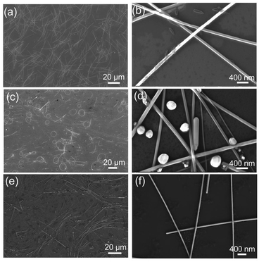 | ||
| Fig. 1 SEM images of AgNWs synthesized with various halogen ions additives: (a and b) 30 μM Cl− ions, (c and d) 30 μM Br− ions, (e and f) a combination of 15 μM Cl− and 15 μM Br− ions. | ||
Under reaction conditions at 130 °C for 8 h, the morphology of AgNWs was controlled by adjusting the concentration of Br− ions in the presence of Cl− ions (15 μM). As the Br− concentration increases from 10 μM (Fig. 2a) to 15 μM (Fig. 2b), the length of AgNWs increases while the diameter decreases. Br− ions preferentially adsorb to the Ag (100) planes, occupying the reduction sites of Ag+ ions and restricting lateral growth, thus promoting axial growth along the Ag (111) planes. Consequently, the aspect ratio of AgNWs increases with increasing Br− concentration. However, as shown in Fig. 2c and d, when the Br− concentration exceeds 15 μM, the length of AgNWs shortens, and the purity significantly decreases due to the excessive Br− ions. Excess Br− ions adsorb onto the Ag (111) planes, causing passivation and inhibiting axial growth. Furthermore, excess Br− ions combine with dissolved oxygen to form Br−/O2,32,33 which aggressively etches multiple twins, resulting in a reduced yield of AgNWs.
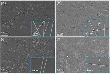 | ||
| Fig. 2 SEM images of AgNWs synthesized with varying Br− concentrations: (a) 10 μM, (b) 15 μM, (c) 20 μM, and (d) 50 μM. The insets depict magnified views of corresponding images. | ||
Building upon the optimized results, the influence of Cl− ion concentration was examined to refine the morphology of AgNWs. Among the samples prepared with Cl− ion concentrations of 15 μM (Fig. 3a and b), 30 μM (Fig. 3c and d), and 45 μM (Fig. 3e and f), those depicted in Fig. 3c and d exhibit the longest AgNWs, measuring 100 μm in length, and the smallest diameters, approximately 45 nm. Similar to Br− ions, increasing the concentration of Cl− ions can suppress radial growth and enhance axial elongation of the nanowires. However, excessive Cl− ions may interfere with nanowire formation, leading to the formation of short rods or even particles.
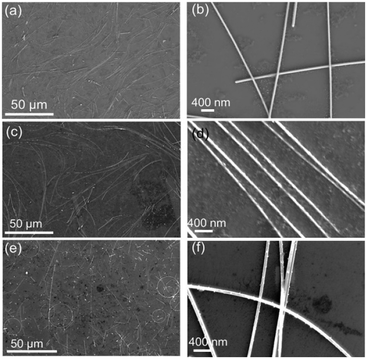 | ||
| Fig. 3 SEM images of AgNWs synthesized with different Cl− concentrations: (a and b) 15 μM, (c and d) 30 μM, and (e and f) 45 μM. | ||
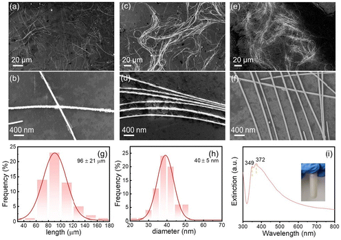
Through the synergistic action of Cl− and Br− ions, AgNWs with an aspect ratio of approximately 2200 can be synthesized, as depicted in Fig. 3c and d. To enhance the aspect ratio further, we finely tuned the reaction conditions by modifying the temperature from 130 °C to 145 °C and the reaction time from 8 h to a range of 4–6 h to govern the growth of the nanowires. As the reaction duration extends from 4 h (Fig. 4a and b) to 5 h (Fig. 4c and d), the AgNWs increase in length with a diameter that remains largely unchanged. However, when the reaction time is prolonged to 6 h (Fig. 4e and f), the length stabilizes while the diameter shows an increase. Notably, the AgNWs produced at 145 °C for 5 h demonstrate the longest average length of 96 μm (Fig. 4g) and the finest average diameter of 40 nm (Fig. 4h), yielding an aspect ratio as high as 2400. The UV-Vis absorption spectrum in Fig. 4i reveals extinction peaks at 372 nm, with a shoulder peak observable at 349 nm. The 372 nm peak corresponds to the transverse LSPR mode of the AgNWs, while the shoulder peak at 349 nm resembles the plasmonic peak typically seen in silver thin films.24,34,35 The absence of absorption peaks in the 400–470 nm range, which are characteristic of silver nanoparticles, confirms the high purity of the AgNWs in the final product.
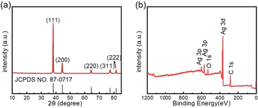
To assess the crystallinity of the synthesized AgNWs, we conducted XRD analysis. As depicted in Fig. 5a, the diffraction peaks observed at 38.1°, 44.2°, 64.4°, 77.4°, and 88.5° correspond to the Ag (111), (200), (220), (311), and (222) crystal planes (JCPDS no. 04-0783), respectively, which confirms the face-centered cubic structure of silver. Additionally, XPS analysis was performed to examine the elemental composition of the AgNWs. In the XPS survey spectrum shown in Fig. 5b, despite the O 1s and C 1s peaks originating from PVP capping agent, the distinct Ag 3d and 3p peaks are prominently displayed, signifying the purity of the silver composition in the product.
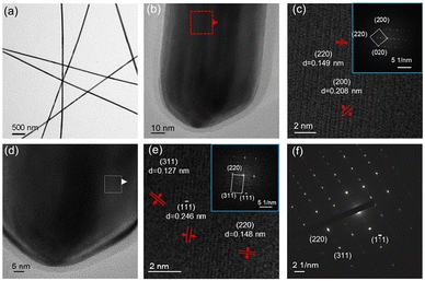
The TEM image in Fig. 6a confirms the thin diameter of the AgNWs, in alignment with SEM observations. A high resolution TEM (HRTEM) image of the side region of the AgNWs is presented in Fig. 6b. Fig. 6c zooms in on the selected area to show lattice fringes with interplanar spacings of 0.208 nm and 0.149 nm, corresponding to the silver (200) and (220) planes, respectively. The inset in Fig. 6c displays the Fast Fourier Transform (FFT) pattern from the region, showing diffraction spots 200 and 220 corresponding to (200) and (220) planes, respectively. The measured angle of 44.63° between (200) and (220) planes closely matches the theoretical angle of 45.0°, identifying the crystal zone axis as [001]. FFT analysis also indicates the presence of diffraction spots from multiple twin structures within the AgNWs.
In the top region of the AgNWs (Fig. 6d and e), lattice fringes with spacings of 0.246 nm, 0.148 nm, and 0.127 nm are observed, corresponding to the (1![[1 with combining macron]](https://www.rsc.org/images/entities/char_0031_0304.gif) 1), (220), and (311) crystal planes of Ag(face-centered cubic). The FFT diagram inset in Fig. 6e shows diffraction spots for 220, 311 and 1
1), (220), and (311) crystal planes of Ag(face-centered cubic). The FFT diagram inset in Fig. 6e shows diffraction spots for 220, 311 and 1![[1 with combining macron]](https://www.rsc.org/images/entities/char_0031_0304.gif) 1, which assign to (220), (311) and (1
1, which assign to (220), (311) and (1![[1 with combining macron]](https://www.rsc.org/images/entities/char_0031_0304.gif) 1) planes. The angles between the (1
1) planes. The angles between the (1![[1 with combining macron]](https://www.rsc.org/images/entities/char_0031_0304.gif) 1) and (311) planes and between the (311) and (220) planes are measured as 58.51° and 32.28°, respectively, closely aligning with the theoretical angles of 58.51° and 31.48°, indicating the crystal zone axis as [112]. Non-integer diffraction spots in the FFT pattern suggest twinning within the crystalline structure. The selected area electron diffraction pattern in Fig. 6f exhibits clear spots, indicative of the good crystallinity of the AgNWs. Additionally, the presence of diffraction spots at non-integer positions underscores the twinned nature of the AgNWs crystalline structure.
1) and (311) planes and between the (311) and (220) planes are measured as 58.51° and 32.28°, respectively, closely aligning with the theoretical angles of 58.51° and 31.48°, indicating the crystal zone axis as [112]. Non-integer diffraction spots in the FFT pattern suggest twinning within the crystalline structure. The selected area electron diffraction pattern in Fig. 6f exhibits clear spots, indicative of the good crystallinity of the AgNWs. Additionally, the presence of diffraction spots at non-integer positions underscores the twinned nature of the AgNWs crystalline structure.
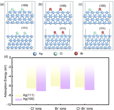
DFT calculations provide insights into how halogen ions (Cl− and Br−) promote the anisotropic growth of AgNWs, controlling their morphology. The DFT models for the adsorption of Cl− ions, Br− ions, and Cl−–Br− ions mixtures on Ag (100) and Ag (111) surfaces are depicted in Fig. 7a–c, respectively, and the coordinates of the halogen ions in these models after structural optimization can be find in Table S5 of the ESI.† Top views of these models are in Fig. S1 of the ESI.† The adsorption energies for Cl−, Br−, and Cl−–Br− combination on these silver surfaces are calculated and presented in Fig. 7d. On the Ag (100) plane, the adsorption energies are −7.13 eV for Cl−, −6.66 eV for Br−, and −6.90 eV for Cl−–Br−. On the Ag (111) plane, the adsorption energies of Cl−, Br− and Cl−–Br− are −6.50 eV, −6.05 eV and −6.28 eV, respectively. The adsorption energy reflects the surface binding ability of halogen ions and silver. The larger the adsorption energy, the stronger the binding ability of halogen ion and silver surface, the stronger the ability to hinder the growth of silver.36,37 The adsorption energies for all three ion combinations are higher on the Ag (100) plane, suggesting a greater occupancy of reactive sites and a hindered deposition of Ag+ ions. This preferential adsorption is thought to direct the anisotropic growth of silver nuclei.
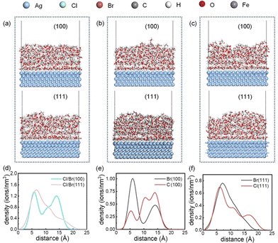
Traditionally, DFT calculations have limited consideration for solvent effects when simulating the growth of silver nanostructures. Luckly, MD simulations have proven to be valuable in exploring interactions at the solid–liquid interface.38,39 To gain a more comprehensive understanding of the adsorption behavior of solvated ions on the Ag (100) and Ag (111) surfaces, MD simulations were utilized to model the adsorption of Cl− and Br− ions on these surfaces. Fig. S2–S7 in the ESI† shows the calculation model and the simulation process for Ag (100) and Ag (111) planes under different ions combinations. Fig. 8a–c offer a 2000 ps snapshot from the MD simulations, showcasing six distinct models with Cl−, Br−, and Cl−–Br− mixtures adsorbed on both the Ag (100) and Ag (111) surfaces, and the distribution density of ions on the silver surface is obtained from molecular dynamics simulations. Fig. 8d highlights the presence of two ions solvation sheath with equivalent ion density on the Ag (100) surface in the Cl−–Br− mixed system, in contrast to a single ions solvation sheath on the Ag (111) surface. Under the influence of two solvation sheath, a higher ion distribution density or a greater number of solvation sheath will more effectively slow down the growth of silver.31,40,41 Thus, the growth rate on the Ag (100) surface is further reduced, thereby intensifying the anisotropic growth of silver nanowires.
The adsorption density distributions of Cl− and Br− ions on the Ag (100) and Ag (111) surfaces are depicted in Fig. S8.† The greater the difference in ion density distribution, the more significant the difference in the growth rates on the two surfaces. Both ions exhibit higher adsorption density on the Ag (100) surface compared to the Ag (111) surface, with the Cl− density difference being more pronounced, indicating that Cl− ions have a stronger effect in promoting the anisotropic growth of AgNWs compared to Br− ions, thus being more conducive to the formation of AgNWs. Fig. 8e and f display the adsorption density of Cl− and Br− ions on the Ag (100) and Ag (111) planes within the mixed system. On the Ag (100) plane, the Br− ions solvation sheath is closer to the silver surface and has a higher density compared to the Cl− layer. On the Ag (111) plane, the adsorption densities of Cl− and Br− are similar, with similar solvation sheath. These findings indicate that compared to the influence of Cl− ions, the lateral growth rate of AgNWs composed of the Ag{100} family of crystal facets is slower under the action of Br− ions, playing an essential role in controlling the reduction of the silver nanowire diameter.
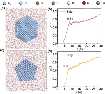
MD simulations were used to simulate the adsorption of the Cl− and Br− hybrid system on AgNWs. The simulation snapshots and total energy evolution curve are detailed in Fig. S9.†Fig. 9a presents a 1200 ps snapshot of the side of AgNWs, and Fig. 9b shows the corresponding radial distribution function (g(r)). At the first peak position, g(r) = 0.81. Fig. 9c illustrates a 1200 ps snapshot of halogen ions distribution on the top of AgNWs, and Fig. 9d displays the g(r) at the first peak, which is 0.65. The MD simulation reveals that halogen ions exhibit a higher density distribution along the radial direction (Ag {100}) compared to the longitudinal direction (Ag {111}) of AgNWs. This leads to a slower reduction and deposition rate of Ag+ on the Ag {100}planes, with Ag+ preferentially depositing on the Ag {111} planes, thereby facilitating the formation of AgNWs.
In summary, DFT calculations reveal a difference in the adsorption energy of halogen ions on the Ag (100) and Ag (111) planes, with a stronger adsorption on the Ag (100), indicating a preference for halogen ion adsorption on this plane. MD simulations further confirm that the adsorption and passivation effect of halogen ions is stronger on the Ag (100) than on the Ag (111). These findings collectively suggest that halogen ions promote the anisotropic growth of multiple twins, leading to the formation of AgNWs. Additionally, MD results indicate that Cl− ions are more effective in promoting the formation of AgNWs, and the higher adsorption density of Br− ions on the radial direction of AgNWs is favorable for the formation of smaller diameter AgNWs.
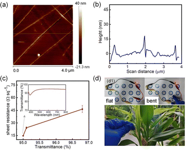
Inks were prepared by incorporating various concentrations of the synthesized AgNWs, which were then used to fabricate TCFs using the Meyer rod technique. AFM images in Fig. 10a and b show the TCF and the distribution of AgNWs, indicating a relatively uniform nanowire distribution and an even film surface with an average roughness (Ra) of 2.06 nm. Fig. 10c depicts the relationship between transmittance and sheet resistance, showing that as transmittance is 95.0%, the sheet resistance can be as low as 14.7 Ω sq−1. Notably, the light transmittance increases with an increase in sheet resistance. Table S6† offers a comparative analysis of our research against the latest studies, highlighting critical performance metrics including the dimensional characteristics and aspect ratios of AgNWs, as well as the sheet resistance and optical transmittance of TCFs. The findings underscore a clear and pronounced superiority in our approach.
The UV-Vis spectrum of the inset in Fig. 10c indicates that the TCF exhibits high light transmittance in the visible range. Fig. 10d1 display the LED connected to the TCF circuit. The luminance of the LED remains stable regardless of whether the TCF is flat or bent, demonstrating the robust electrical conductivity of the TCF even when deformed. Fig. 10d2 further illustrates the high light transmittance of the TCF. In addition to their attributes of high light transmission and low sheet resistance, the extensive utility of flexible TCFs necessitates superior mechanical robustness. These films must endure repeated bending without compromising their functional integrity, which is crucial for their integration into a diverse range of applications, from wearable electronics to foldable displays.42–45 The bending test shown in Fig. S10a† was performed as follows: initially, the TCF was folded with radius of 6 mm in one direction, followed by folding it in the opposite direction, thereby completing a single cycle. The variations in sheet resistance and transmittance throughout the severe bending procedure are represented in Fig. S10b.† Throughout the 1000 cycles, the sheet resistance and transmittance of the TCF only change slightly. These findings indicate that the TCF has superior flexibility and robust application reliability.
The TCF was shaped into a 20 mm × 35 mm rectangle and a heating element was created by attaching copper electrodes to the ends. An 8 V working voltage was applied to assess the defogging and heating capabilities of the film. Fig. 11a demonstrates the defogging efficiency of the film with a sheet resistance of 14.7 Ω sq−1. It can remove water mist within 30 seconds, which is 30 times faster than natural drying. The defogging performances of films with sheet resistances of 24.2 Ω sq−1 and 46.5 Ω sq−1 are shown in Fig. S11.† The results indicate that films with lower sheet resistance remove water mist more quickly. Fig. 11b shows that the film temperature reaches 121.2 °C after 10 seconds of powering on and exceeds 150 °C after 50 seconds. The film gradually cools down after power is cut off. The heating film exhibits rapid response, with a heating rate of up to 12.1 °C s−1 in the initial 10 seconds. The combination of high transparency and rapid heating makes the film suitable for flexible electronic applications, such as flexible sensing and displays.
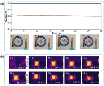 | ||
| Fig. 11 (a) Defogging efficiency of TCFs with a sheet resistance of 14.7 Ω sq−1. (b) Infrared thermal imaging of heating performance of the TCFs heater. | ||
Conclusions
We have successfully synthesized AgNWs with an aspect ratio exceeding 2400, achieving lengths of 96 μm and diameters of 40 nm, through careful optimization of Cl− and Br− ion concentrations and leveraging their synergistic effects. DFT and MD simulations have elucidated the following key findings: (1) halogen ions exhibit a stronger affinity for the Ag (100) surface. (2) Cl− ions are more effective in promoting the formation of AgNWs, while Br− ions have a more pronounced effect in constraining nanowire diameter, favoring the synthesis of AgNWs with smaller diameters. The TCFs fabricated with these AgNWs exhibit exceptional optical and electrical performance, with a light transmittance of 95.0% at 550 nm and a sheet resistance of 14.7 Ω sq−1. The TCFs used as heating films demonstrate a rapid response rate of 12.1 °C s−1, capable of reaching temperatures above 150 °C within 50 seconds. These results indicate that the high aspect ratio AgNWs are critical for enhancing TCF performance and expanding their potential applications in wearable electronics.Experimental section
Chemicals
All the chemicals are used without any further purification. Silver nitrate (AgNO3, AR) was obtained from Sinopharm Chemical Reagent Co., Ltd poly(vinylpyrrolidone) (PVP, MW = 1![[thin space (1/6-em)]](https://www.rsc.org/images/entities/char_2009.gif) 300
300![[thin space (1/6-em)]](https://www.rsc.org/images/entities/char_2009.gif) 000) was purchased from Shandong Yousuo Chemical Technology Co., Ltd. Ethylene glycol (EG, AR) was gained from Shanghai Titan Scientific Co., Ltd. Sodium chloride (NaCl, 99.5%), sodium bromide (NaBr, 99.0%), ferric chloride hexahyrate (FeCl3·6H2O, 98%), and ethanol (C2H5OH, AR) were purchased from Chengdu Chron Chemical Co., Ltd. Ferric bromide (FeBr3, 98%) was purchased from Tianjin Heowns Optus Technology Co., Ltd. Carboxymethyl cellulose sodium (CMC-Na) was gained from Aladdin. The deionized water used in experiments has a conductivity of less than 0.055 μS cm−1. Polyethylene terephthalate (PET), with a thickness of 150 μm, was used as the substrate for TCFs.
000) was purchased from Shandong Yousuo Chemical Technology Co., Ltd. Ethylene glycol (EG, AR) was gained from Shanghai Titan Scientific Co., Ltd. Sodium chloride (NaCl, 99.5%), sodium bromide (NaBr, 99.0%), ferric chloride hexahyrate (FeCl3·6H2O, 98%), and ethanol (C2H5OH, AR) were purchased from Chengdu Chron Chemical Co., Ltd. Ferric bromide (FeBr3, 98%) was purchased from Tianjin Heowns Optus Technology Co., Ltd. Carboxymethyl cellulose sodium (CMC-Na) was gained from Aladdin. The deionized water used in experiments has a conductivity of less than 0.055 μS cm−1. Polyethylene terephthalate (PET), with a thickness of 150 μm, was used as the substrate for TCFs.
Synthesis of AgNWs
In the typical synthesis process of AgNWs, 0.12 g of PVP was dissolved in 20 mL of EG at room temperature. Next, 0.08 g of AgNO3 was introduced into the PVP solution and stirred for 30 min to create a homogeneous mixture. Then, 2 μL of FeCl3 (0.1 M) and 3 μL of NaBr (0.1 M) were added to this mixture with stirring for 10 min. The resulting reaction mixture was then transferred into a 25 mL Teflon-lined stainless-steel autoclave, which was maintained at 145 °C for 5 h. After the reaction, acetone was added to the resulting products at a volume ratio of 1![[thin space (1/6-em)]](https://www.rsc.org/images/entities/char_2009.gif) :
:![[thin space (1/6-em)]](https://www.rsc.org/images/entities/char_2009.gif) 3. After allowing the AgNWs to precipitate, the supernatant was carefully removed. Next, a mixture of deionized water and acetone with a volume ratio of 1
3. After allowing the AgNWs to precipitate, the supernatant was carefully removed. Next, a mixture of deionized water and acetone with a volume ratio of 1![[thin space (1/6-em)]](https://www.rsc.org/images/entities/char_2009.gif) :
:![[thin space (1/6-em)]](https://www.rsc.org/images/entities/char_2009.gif) 3 was introduced into the obtained precipitate, and the supernatant was discarded again after precipitation. Subsequently, deionized water was used to fully disperse the AgNWs, followed by centrifugation at 2000 rpm for 15 min. After removing the supernatant, an additional round of dispersion in deionized water and centrifugation at 1500 rpm for 15 min was performed. The resulting AgNWs were then dispersed in deionized water for subsequent applications.
3 was introduced into the obtained precipitate, and the supernatant was discarded again after precipitation. Subsequently, deionized water was used to fully disperse the AgNWs, followed by centrifugation at 2000 rpm for 15 min. After removing the supernatant, an additional round of dispersion in deionized water and centrifugation at 1500 rpm for 15 min was performed. The resulting AgNWs were then dispersed in deionized water for subsequent applications.
Preparation of TCFs
The as-prepared AgNWs were dispersed into deionized water to achieve a concentration of 2.0 mg mL−1. Subsequently, 0.3 wt% of CMC-Na was incorporated into the dispersion to formulate the AgNWs ink. The ink was then dropped onto a PET substrate that had been pretreated with oxygen plasma. Then the AgNWs coating was obtained by pulling the Meyer rod at a rate of 2–4 cm s−1. Finally, the PET substrate coated with AgNWs was placed in a drying oven at 60 °C for 20 min, resulting in the production of TCFs.Characterization
The morphologies and structure of the AgNWs were examined using scanning electron microscopy (SEM, Apreo2, UK) and transmission electron microscopy (TEM, JEM-2100plus, Japan). The crystal structure of was identified by X-ray diffraction (XRD, D8 ADVANCE, Germany). The chemical composition was analyzed with X-ray photoelectron spectroscopy (XPS, ESCALAB250Xi, UK). The optical properties, including the extinction of AgNWs dispersion and the transmittance of TCFs, were characterized using UV-Vis spectroscopy (Agilent Cary 5000, USA). The surface roughness of TCFs was assessed with atomic force microscopy (AFM, Park Systems Corp, Korea). The sheet resistance was measured using a four-point probe system (RM100A, China). An electrochemical workstation (CHI-660E, China) supplied an 8 V voltage to operate the transparent heating film, while its heating performance was recorded using an infrared thermal imager (PS600, China).Author contributions
Jia-Lei Xu: Methodology, writing – original draft. Rui-Dong Shi: DFT calculation and MD simulation. Haiping Zhou: Film preparation. Guo-Tao Xiang and Zi-Dong Zhou: Investigation. Yong-Da Hu: Validation, project administration. Jin-Ju Chen: Conceptualization, supervision.Data availability
The data supporting this article have been included as part of the ESI.†Conflicts of interest
There are no conflicts to declare.Acknowledgements
This work was supported by Sichuan Science and Technology Program (grant no. 2023YFG0215).References
- Z. Zhao, K. Liu, Y. Liu, Y. Guo and Y. Liu, Natl. Sci. Rev., 2022, 9, nwac090 CAS.
- J. Sun, Y. Chang, J. Liao, S. Chang, S. Dai, Y. Shang, C.-X. Shan and L. Dong, Nano Energy, 2022, 99, 107392 CAS.
- Y. Gao, K. Huang, C. Long, Y. Ding, J. Chang, D. Zhang, L. Etgar, M. Liu, J. Zhang and J. Yang, ACS Energy Lett., 2022, 7, 1412–1445 CrossRef CAS.
- Y. Li, G. Xu, C. Cui and Y. Li, Adv. Energy Mater., 2018, 8, 1701791 CrossRef.
- J. Yang, L. Chang, H. Zhao, X. Zhang, Z. Cao and L. Jiang, InfoMat, 2024, e12529 CrossRef CAS.
- Z. Ma, X. Xiang, L. Shao, Y. Zhang and J. Gu, Angew. Chem., Int. Ed., 2022, 61, e202200705 CrossRef CAS PubMed.
- H. Chen, Y. Jing, J.-H. Lee, D. Liu, J. Kim, S. Chen, K. Huang, X. Shen, Q. Zheng, J. Yang, S. Jeon and J.-K. Kim, Mater. Horiz., 2020, 7, 2378–2389 RSC.
- X. Lin, F. Li, Y. Bing, T. Fei, S. Liu, H. Zhao and T. Zhang, Nano-Micro Lett., 2021, 13, 200 CrossRef CAS.
- W. Gao, S. Emaminejad, H. Y. Y. Nyein, S. Challa, K. Chen, A. Peck, H. M. Fahad, H. Ota, H. Shiraki, D. Kiriya, D.-H. Lien, G. A. Brooks, R. W. Davis and A. Javey, Nature, 2016, 529, 509–514 CrossRef CAS PubMed.
- A. G. Ricciardulli, S. Yang, G.-J. A. H. Wetzelaer, X. Feng and P. W. M. Blom, Adv. Funct. Mater., 2018, 28, 1706010 CrossRef.
- F. L. M. Sam, C. A. Mills, L. J. Rozanski and S. R. P. Silva, Laser Photonics Rev., 2014, 8, 172–179 CrossRef CAS.
- J.-H. Liu and F.-M. Hsieh, Polym. Compos., 2010, 31, 1352–1359 CrossRef CAS.
- D. Shan, L. Liu, Z. Chen, J. Zhang, R. Cui, E. Hong and B. Wang, Arabian J. Chem., 2021, 14, 102978 CrossRef CAS.
- M. Ćwik, D. Buczyńska, K. Sulowska, E. Roźniecka, S. Mackowski and J. Niedziółka-Jönsson, Materials, 2019, 12(5), 721 CrossRef PubMed.
- Y.-J. Zhu and X.-L. Hu, Mater. Lett., 2004, 58, 1517–1519 CrossRef CAS.
- C. Wang, B. Cheng, H. Zhang, P. Wan, L. Luo, Y. Kuang and X. Sun, Nano Res., 2016, 9, 1532–1542 CrossRef CAS.
- J. Jiu, T. Araki, J. Wang, M. Nogi, T. Sugahara, S. Nagao, H. Koga, K. Suganuma, E. Nakazawa, M. Hara, H. Uchida and K. Shinozaki, J. Mater. Chem. A, 2014, 2, 6326–6330 RSC.
- S. M. Bergin, Y.-H. Chen, A. R. Rathmell, P. Charbonneau, Z.-Y. Li and B. J. Wiley, Nanoscale, 2012, 4, 1996–2004 RSC.
- J. Lee, P. Lee, H. B. Lee, S. Hong, I. Lee, J. Yeo, S. S. Lee, T.-S. Kim, D. Lee and S. H. Ko, Adv. Funct. Mater., 2013, 23, 4171–4176 CrossRef CAS.
- J. Li, H. Zhang, H. Yang and S. Lin, Inorg. Chem. Commun., 2023, 158, 111451 CrossRef CAS.
- H. Ao, J. Feng, P. Cao, T. Yang, T. Shang and B. Xing, J. Mater. Sci.: Mater. Electron., 2023, 34, 2183 CrossRef CAS.
- J. Wei, X. Li, F. Bian, J. Zeng, J. Hu, T. Zong, N. Li and S. Lin, Inorg. Chem. Commun., 2022, 146, 110164 CrossRef CAS.
- Y. Sun and Y. Xia, Adv. Mater., 2002, 14, 833–837 CrossRef CAS.
- Y. Sun, Y. Yin, B. T. Mayers, T. Herricks and Y. Xia, Chem. Mater., 2002, 14, 4736–4745 CrossRef CAS.
- Y. Ran, W. He, K. Wang, S. Ji and C. Ye, Chem. Commun., 2014, 50, 14877–14880 RSC.
- K. Sheng Lau, S. X. Chin, S. T. Tan, F. S. Lim, W. Sea Chang, C. Chin Yap, M. H. H. Jumali, S. Zakaria, S. W. Chook and C. H. Chia, J. Alloys Compd., 2019, 803, 165–171 CrossRef CAS.
- K. E. Korte, S. E. Skrabalak and Y. Xia, J. Mater. Chem., 2008, 18, 437–441 RSC.
- S. Wang, Y. Tian, S. Ding and Y. Huang, Mater. Lett., 2016, 172, 175–178 CrossRef CAS.
- N. Almora-Barrios, G. Novell-Leruth, P. Whiting, L. M. Liz-Marzán and N. López, Nano Lett., 2014, 14, 871–875 CrossRef CAS PubMed.
- N. Xiao, Y. Chen, W. Weng, X. Chi, H. Chen, D. Tang and S. Zhong, Nanomaterials, 2022, 12(15), 2681 CrossRef CAS.
- S. K. Meena and M. Sulpizi, Angew. Chem., Int. Ed., 2016, 55, 11960–11964 CrossRef CAS PubMed.
- Y. Zheng, J. Zeng, A. Ruditskiy, M. Liu and Y. Xia, Chem. Mater., 2014, 26, 22–33 CrossRef CAS.
- B. Wiley, T. Herricks, Y. Sun and Y. Xia, Nano Lett., 2004, 4, 1733–1739 CrossRef CAS.
- Y. Shi and J. Fang, J. Phys. Chem. C, 2022, 126, 19866–19871 CrossRef CAS.
- Y. Li, X. Yuan, H. Yang, Y. Chao, S. Guo and C. Wang, Materials, 2019, 12, 401 CrossRef CAS.
- K. C. Jha, H. Liu, M. R. Bockstaller and H. Heinz, J. Phys. Chem. C, 2013, 117, 25969–25981 CrossRef CAS.
- L. Huang, G. Li, Y.-Y. Zhang, L.-H. Bao, Q. Huan, X. Lin, Y.-L. Wang, H.-M. Guo, C.-M. Shen, S.-X. Du and H.-J. Gao, Acta Phys. Sin., 2018, 67, 126801–126801 CrossRef.
- R. Wang, M. L. Klein, V. Carnevale and E. Borguet, Wiley Interdiscip. Rev.: Comput. Mol. Sci., 2021, 11, e1537 CAS.
- X.-T. Fan, X.-J. Wen, Y.-B. Zhuang and J. Cheng, J. Energy Chem., 2023, 82, 239–247 CrossRef CAS.
- S. K. Meena and M. Sulpizi, Langmuir, 2013, 29, 14954–14961 CrossRef CAS PubMed.
- J. A. da Silva, P. A. Netz and M. R. Meneghetti, Langmuir, 2020, 36, 257–263 CrossRef CAS PubMed.
- X. Lu, Y. Zhang and Z. Zheng, Adv. Electron. Mater., 2021, 7, 2001121 CrossRef CAS.
- L. He and S. C. Tjong, Mater. Sci. Eng., R, 2016, 109, 1–101 CrossRef.
- L. Gan, Y. Liu, X. Yang, J. Chen, N. Yang and Y. Zhu, Crit. Rev. Solid State Mater. Sci., 2024, 1–53, DOI:10.1080/10408436.2024.2379246.
- T. Sannicolo, M. Lagrange, A. Cabos, C. Celle, J.-P. Simonato and D. Bellet, Small, 2016, 12, 6052–6075 CrossRef CAS.
Footnote |
| † Electronic supplementary information (ESI) available: Modeling parameters, theoretical calculation data and heating performance. See DOI: https://doi.org/10.1039/d4nr03525a |
| This journal is © The Royal Society of Chemistry 2025 |

