
Refined design of a DNA logic gate for implementing a DNA-based three-level circuit†
Yuanpeng
Zhang‡
ce,
Bei
Yan‡
bc,
Xingge
Li
f,
Huan
Liu
c,
Xiao
Liu
c,
Xianjin
Xiao
 *cd,
Zenghui
Mao
*d and
Zhihao
Ming
*a
*cd,
Zenghui
Mao
*d and
Zhihao
Ming
*a
aDepartment of Urology, Hunan Cancer Hospital/The Affiliated Cancer Hospital of Xiangya School of Medicine, Central South University, Changsha, China. E-mail: mingzhihao@hnca.org.cn
bDepartment of Human Sperm Bank, Institute of Medical Science, General Hospital of Ningxia Medical University, Yinchuan, Ningxia 750004, China
cInstitute of Reproductive Health, Tongji Medical College, Huazhong University of Science and Technology, Wuhan 430030, China. E-mail: xiaoxianjin@hust.edu.cn
dHunan Provincial Key Laboratory of Regional Hereditary Birth Defects Prevention and Control, Changsha Hospital for Maternal & Child Health Care Affiliated to Hunan Normal University, Changsha, China, zhmao48@163.com
eDepartment and Institute of Urology, Union Hospital, Tongji Medical College, Huazhong University of Science and Technology, Wuhan 430030, China
fDepartment of Gastroenterology, Union Hospital, Tongji Medical College, Huazhong University of Science and Technology, Wuhan, 430022, China
First published on 6th November 2024
Abstract
DNA computing circuits are favored by researchers because of their high density, high parallelism, and biocompatibility. However, compared with electronic circuits, current DNA circuits have significant errors in understanding the OFF state and logic “0”. Nowadays, DNA circuits only have two input states: logic “0” and logic “1”, where logic “0” also means the OFF state. Corresponding to an electronic circuit, it is more like an on–off switch than a logic circuit. To correct this conceptual confusion, we propose a three-level circuit. The circuit divides the input signal into three cases: “none”, logic “0” and logic “1”. In subsequent experiments, 34 input combinations of the primary AND gate, OR gate as well as secondary AND–OR and OR–AND cascade circuits were successfully implemented to perform the operation, which distinguished the OFF state and logic “0” correctly. Based on this, we successfully implemented a more complex voting operation with only 12 strands. We believe that our redefinition of the OFF state and logic “0” will promote tremendous developments in DNA computing circuits.
Introduction
In electronic circuits, silicon has become the cornerstone owing to its outstanding semiconductor electrical properties and chemical stability.1 However, the poor biocompatibility of silicon greatly limits its application in biomedicine.2 Therefore, novel DNA circuits with high biocompatibility have been proposed.3–5 In the past decade, DNA circuits have made significant progress in various aspects, from constructing basic logic components to designing complex combinational and sequential logic circuits.6–8 DNA circuits have considerable processing capabilities. Researchers have successfully implemented various powerful DNA circuits, including adders,9 subtractors,10 and arithmetic logic units (ALUs).11–15 With a deeper understanding of DNA circuits, researchers have attempted to simulate biological neural networks to achieve advanced information processing and pattern recognition. Artificial neural networks based on DNA circuits have been designed.16–18 These DNA neural networks have been successfully applied in fields such as classification,19,20 diagnosis,9,20,21 and control,22,23 demonstrating high flexibility and scalability.17,24 In addition, by leveraging DNA self-assembly, researchers have developed DNA circuits with self-healing,25 adaptive26 and programmable features.27 Thus, remarkable progress has been made in DNA circuits.However, there is a fundamental difference in electronic circuits and traditional DNA circuits: The traditional DNA logic circuits completely conflate the input “none” and logic “0”.3–5 As shown in Fig. 1 (up), in traditional DNA logic circuits, there are only two states: logic “0” and “1”, where the input “none” and logic “0” are equivalent. This conflation has brought many bottlenecks to the field of DNA circuits. Firstly, once circuit assembly is completed, even without any actual input, the circuit is already in an operational state because the input “none” and logic “0” are equivalent. This leads to the inability to construct the NOT gate, which plays an important role in electronic circuits. NOT gates are crucial for simplifying circuits and modular circuit assembly. To compensate for this deficiency, researchers can only use a dual track mode to achieve the NOT gate function. A dual track mode significantly increases circuit complexity and cannot support circuit module assembly through NOT logic, which goes against the inherent advantages of NOT gates in electronic circuits.3 Secondly, since the circuit is in an operational state without actual inputs, there is no OFF state, unlike the OFF state in electronic circuits. This requires stringent restrictions on leakage before reaction activation, posing greater challenges for the already difficult leakage prevention.28–30 In summary, existing DNA monorail circuits cannot distinguish between input “none” and input logic “0”, so there is no actual OFF state, thus greatly limiting the development of more complex and practical DNA circuits.
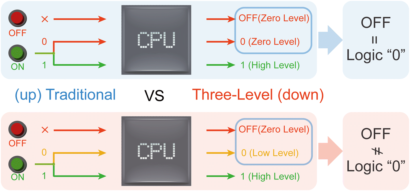 | ||
| Fig. 1 Contrast of a traditional DNA circuit and three-level DNA circuit. As shown in figure (top), state “OFF” and logic “0” represent the same situation in the traditional DNA circuit (displayed with a red line and blue frame). As shown in figure (bottom), state “OFF” and logic “0” represent the different situation in the three-level DNA circuit (state “OFF” is displayed with a red line and logic “0” is displayed with an orange line). The buttons “OFF” and “ON” represent the different states of the circuit. The element “CPU” represents the process of calculation. | ||
Herein, we proposed a new DNA logic circuit signal mode, named three-level circuits. Three-level circuits divided the signal into three scenarios: zero level, low level, and high level, corresponding to the OFF state, logic “0”, and logic “1”, as shown in Fig. 1 (down). In subsequent experiments, a total of 34 input combinations, including the AND gate, OR gate, and AND–OR, OR–AND cascade circuits, were successfully enabled to perform operations that correctly distinguish the OFF state and logic “0”. On this basis, we further implemented a voting operation, which is more powerful but simplified. We believe that our redefinition of the OFF state and logic “0” will greatly promote the development of DNA circuits.
Materials and methods
Materials
The unlabelled DNA strands were synthesized and purified by HAP (Sangon Co., China) while the fluorophore and quencher-labelled strands were synthesized and purified by HPLC (Sangon Co., China). The sequences of all the probes and targets that have been used in this work are summarized in Table S1.† The concentration of each strand was quantified by a Nanodrop 2000c spectrophotometer (Thermo Fisher). RNase-free deionized water from Sangon Co. was used in all the experiments. All the DNA oligonucleotides were ordered in dry format and suspended in Tris–EDTA buffer (10 mM Tris-HCl and 1 mM EDTA pH 8.0). The Bst DNA Polymerase, Large Fragment (#M0275L) and dNTP (#N0447L) were all purchased from New England Biolabs (MA, USA).Time-based fluorescence data acquisition
Time-based fluorescence data were acquired using Synergy HTX Multi-Mode Microplate Reader (BioTek, USA). We set the excitation wavelength at 485 nm and emission wavelength at 528 nm for the FAM fluorophore. The duration of fluorescence acquisition varies. Typically, we set a maximum acquisition duration of 2 hours but terminate the experiment early if the increasing rate of the fluorescence signal remained stable and could be calculated precisely (to facilitate the more rapid collection of data). Time 0 in kinetic plots represents the moment the first data point was measured.Reaction system preparation
To prepare the reaction system, first, we mixed the substrate strands and the fuel strands at 1![[thin space (1/6-em)]](https://www.rsc.org/images/entities/char_2009.gif) :1 ratio with 8 units Bst DNA polymerase, 2 μL dNTP, 1× reporter and 1× ThermoPol reaction buffer (New England Biolabs). Then, we incubated the system at 37 °C for 10 min to make the Bst DNA polymerase extend the output strands successfully. Finally, we added the inputs we needed and started the fluorescence detection. The reporter is mixed with 1× FAM and 1× BHQ and heated to 85 °C for 5 minutes and then to 55 °C for 3 minutes and then cooling to 25 °C with at the rate of 0.1 °C s−1 before the experiment.
:1 ratio with 8 units Bst DNA polymerase, 2 μL dNTP, 1× reporter and 1× ThermoPol reaction buffer (New England Biolabs). Then, we incubated the system at 37 °C for 10 min to make the Bst DNA polymerase extend the output strands successfully. Finally, we added the inputs we needed and started the fluorescence detection. The reporter is mixed with 1× FAM and 1× BHQ and heated to 85 °C for 5 minutes and then to 55 °C for 3 minutes and then cooling to 25 °C with at the rate of 0.1 °C s−1 before the experiment.
Kinetic experiments
To a 200 μL PCR tube, the substrate strands, the fuel strands, the input strands, the reporter, the blocker, the Bst DNA polymerase, the dNTP and ThermoPol buffer were added and brought up to a total volume of 50 μL by deionized water. All the samples were mixed and prepared at room temperature. The solutions were immediately put into a Synergy HTX Multi-Mode Microplate Reader (BioTek, USA) for fluorescence measurement.Fluorescence data analysis
All raw data acquired by the Synergy HTX Multi-Mode Microplate Reader (BioTek, USA) were exported to an EXCEL file, which was subsequently imported, analysed, and plotted using ORIGIN and GraphPad. Time was linearly adjusted so that t = 0 corresponds to the first data point acquired after the PCR tubes were put into the machine after the addition of reagents. For each curve, the fluorescence data were usually normalized using the background fluorescence intensity as “0” and the positive control fluorescence intensity (average of the last five data points) as “1”. The signal-to-noise ratio (SNR) is obtained by dividing the fluorescence signal of the desired reaction when the signal reached the plateau value by that of the leak. If the signal cannot reach the plateau value, SNR is obtained by dividing the fluorescence signal of the desired reaction at the end of the experiment by that of the leak. No additional adjustments are made to the raw fluorescence kinetic plots.Results
Basic DNA logic gates
No matter how complex a DNA circuit is, its basic components are AND and OR gates; thus, we need to implement the three-level current mentioned above at the level of basic logic components. As shown in Fig. 2a, we conducted the experiment according to this process. All elements in the “reaction system” and substrate strands were pre-incubated in 37 °C for 10 minutes; then, the inputs were added and put into the microplate reader as soon as possible.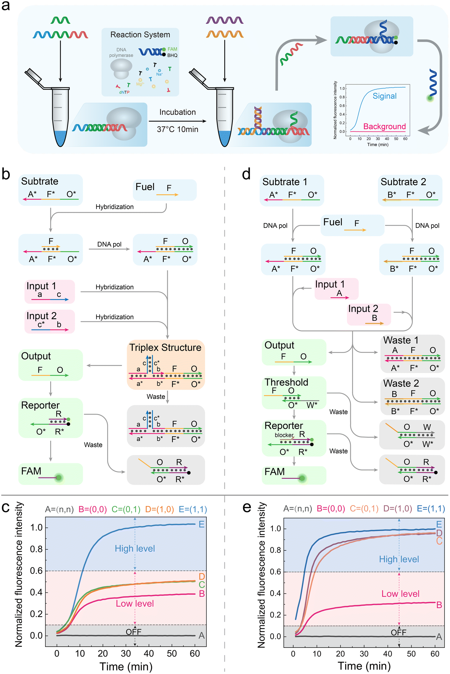 | ||
| Fig. 2 The basic DNA logic gates of the three-level circuit. (a) The procedures of operations and reactions. First, the RNase-free ddH2O, dNTP, DNA polymerase, the reporter (double strands with FAM and BHQ) and the reaction buffer (contains 0.05 M Na+, 0.002 M Mg2+ and so on) were mixed. Then, the substrates and fuel were put into the system. After 10-minute incubation at 37 °C, inputs were added. Finally, the whole volume of 50 μL was put into a microplate reader to start the reaction and detect, still at 37 °C. (b) The intended reaction process of the AND gate. The concentration of substrate “O*F*A*”, fuel “F” and reporter “R*O*/R” were 150 nM. Sequence “A*” consisted of “a*” and “b*” and matched with input 1 “ac” and input b “c*b”, respectively. (c) It showed the normalized results of the three-level AND gate. The method of normalization is displayed in the “Materials and methods” section. (d) The intended reaction process of the OR gate. The concentration of substrate 1 “O*F*A*”, substrate 2 “O*F*B*”, and reporter “R*O*/R” were 150 nM, the fuel was 300 nM. Input 1 “A” and input 2 “B” matched with substrate 1 and 2, respectively. (c and e) Normalized kinetics of the three-level AND gate and the OR gate. Curves “A–E” correspond to different combinations of inputs that are showed above the diagrams, and they are labelled with the same colour. The letter “n” of combination A means “no input 1/no input 2”. “DNA pol” means DNA polymerase. The boundary of “OFF”, “low level” and “high level” were 0.1 and 0.6, based on statistical analysis. The method of normalization is displayed in the “Materials and methods” section, and all the data standardization in this article has been carried out accordingly. All experiments depicted in the figure were replicated at least three times. | ||
In the AND gate, as shown in Fig. 2b, we first added substrate A*F*O* and fuel strand F and then generated the A*F*O*/FO duplex under the extension of Bst polymerase.5 Two inputs of the AND gate were designed to be partially complementary, and their non-complementary regions were designed to be complementary to the domain A* of the A*F*O*/FO duplex. The lengths of domain a and b are subtly designed so that individual input 1 or input 2 cannot bind to A*F*O* but when both are present, they will form a triplet structure with domain A* of the A*F*O*/FO, and the free 3′-OH end of input 2 can initiate the elongation process by Bst polymerase and displace off the output FO strand. In our experiment, we set logic “0” as 50 nM (low level) and logic “1” as 150 nM (high level). Under a such scenario, when no inputs are present, the circuit will be silent. When both inputs are logic “0”, 50 nM of triplet are formed and elongated, producing 50 nM outputs, corresponding to logic “0”. When the input 1 is logic “0” and input 2 is logic “1” or the vice versa, still 50 nM outputs are produced, corresponding to logic “0”. When both inputs are logic “1”, the amount of triplet will be 150 nM, producing 150 nM outputs, corresponding to logic “1”. The signal input form is shown in ESI Fig. S1.† Overall, the truth table of our established AND gate is correct, demonstrating the feasibility of constructing three-level current AND gates (Table S1†). The AND gate was tested under five reasonable input combinations, and the outputs were consistent with the truth table. All reactions completed within 20 minutes (Fig. 2c). Also, the details of the triplet were shown in Fig. S2.† We would discuss the division among “OFF”, “low level”, and “high level” later.
In the OR gate, as shown in Fig. 2d, fuel strand F is first incubated with two substrates, which is consistent with the AND gate. Input 1 and input 2 were designed to be completely complementary to the domain A* of substrate 1 and domain B* of substrate 2, respectively. After adding the inputs, the displaced FO strands will be consumed by the threshold strands W*O* firstly and then the residual FO strands can react with reporter. In accordance with the AND gate, we set logic “0” as 50 nM (low level) and logic “1” as 150 nM (high level). Besides, the concentration of threshold strands and blocker strands were the same as logic “0” and logic “1” respectively. Under such scenario, when no inputs are present, the circuit will be silent. When both inputs are logic “0”, 100 nM of the output FO strand was produced. Then, 50 nM of them are consumed by threshold W*O*, with 50 nM final remaining outputs, which is corresponded to logic “0”. When input 1 is logic “0” and input 2 is logic “1” or the vice versa, 200 nM of output FO strands can be produced, among which 50 nM are consumed by threshold and 150 nM are eventually outputted, which corresponded to logic “1”. When both inputs are logic “1”, the final output can be 250 nM, but the downstream are all fixed at 150 nM. Therefore, the output strands entering the downstream gates are also 150 nM, which corresponded to logic “1”. To sum up, the OR gate can also match the correct truth table theoretically (Table S2†). Similarly, following the process shown in Fig. 2a, we tested the OR gate under 5 reasonable input combinations. The results completely matched the truth table, and the reactions reached the platform within 20 minutes (Fig. 2e).
By constructing basic AND and OR gates, we have achieved the distinction between the OFF state and logic “0” successfully. It provides us a more flexible, stable, and scalable foundation for subsequent DNA circuit design.
Optimization of the AND gate
The key to constructing a three-level AND gate is the triplet structure. The triplet consists of input 1, input 2, and the substrate. Neither input 1 nor input 2 can react with the substrate independently. But their dimer can combine with the substrate stably, assembling the triplet that contains an extendable 3′-OH. Based on this, we tried to optimize the design of the triplet to improve the efficiency of AND gates.First, we did theoretical prediction with NUPACK. For input 1, its 3′-OH end was in a free state after binding the substrate; thus, it could not be extended. For input 2, when b ≤ 8 nt, there was almost no interaction between individual b and substrate, which was the main source of leakage. We finished the prediction using NUPACK, and the details are shown in Table S3 and Fig. S3a.† Then, we explored the assembly ratio of triplets with different length of inputs. When the whole matching length a + b ≥ 18 nt (Fig. 3a), the proportion of triplet was over 99% (Tables S4, S5 and Fig. S3b†). Theoretically, the best structure of the triplet must satisfy that a + b ≥ 18 nt and b ≤ 8 nt.
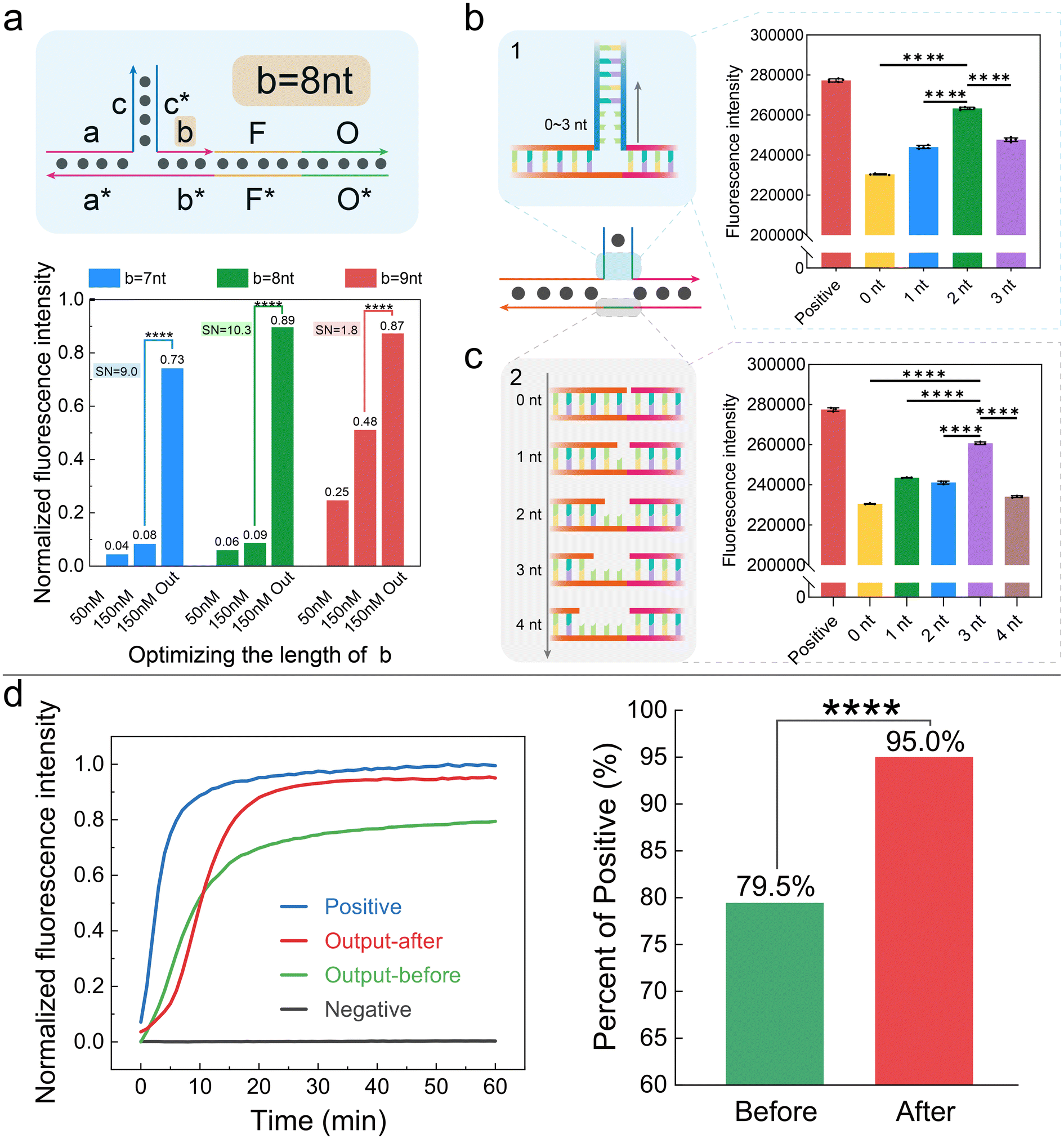 | ||
| Fig. 3 Optimization of the AND gate. (a) Optimize the length of sequence “b”. The above shows the structure of the triplex. Results are displayed below with different lengths of “b”. For each length, 50 nM/150 nM of leakage and 150 nM output were tested. The value right above the column shows the ratio to the positive control. The signal-to-noise ratio with the abbreviation “SN” was chosen as the reference indicator for optimizing the length of sequence “b”. Therefore, 8 nt was selected in the follow-up experiment. (b and c) Optimization of the length of the mismatched base. The left side shows the abstract areas and directions during this optimization. Further, the kinetics process is shown on the right side with colour correspondence. We evaluated the results with the ratio to the positive control. Therefore, 2 nt and 3 nt mismatch were selected for regions 1 and 2 in the follow-up experiment. (d) The kinetics of the three-level AND gate before (green) and after optimization (red). The positive and negative control are shown in blue and black, respectively. Statistical column chart (right) was obtained from the final value of the kinetics. For the positive control, the input was a short strand that matched with the sequence “A” of substrate completely. All experiments depicted in the figure were replicated at least three times (*P < 0.05, **P < 0.01, ***P < 0.001, ****P < 0.0001). | ||
Second, we did experiments to explore which length combination of “a + b” got the best responses. We chose a + b = 18 nt since it was the shortest combination, reducing design difficulty and crosstalk. The experimental results are shown in Fig. 3b. We tested the leakage by adding input 2 only (including situations of 50 nM and 150 nM). We also tested the output when both inputs were added. When the length of segment b was 7 nt, 8 nt, and 9 nt, the signal-to-noise ratio was 9.0, 10.3, and 1.8, respectively. Therefore, we further confirmed that the length of segment b was 8 nt, and the specific experimental results are shown in Fig. S4a and S4b.†
Third, we optimized the junction design to increase the output. The three-level AND gate system was based on the DNA triplet structure. The intersection of input 1, input 2, and substrate might generate significant steric hindrance, affecting triplet stability and causing signal loss. To address this, we designed base mismatches at the triplet intersection. As shown in Fig. 3b, we first inserted “–nA–” bases in sequence c and c* of the inputs, forming a bubble structure to reduce steric hindrance. We synthesized inputs with different mismatch numbers and tested the AND gate signal expression. When mismatches were 0, 1, 2, and 3 nt, the final signal reached 81.0%, 86.4%, 94.0%, and 87.8% of the positive signal, respectively (Fig. 3b and Fig. S4c†). Thus, two mismatches in sequence c and c* minimized signal loss. We also inserted A bases between segments a* and b* of the substrate. As shown in Fig. 3c, three bases minimized AND gate signal loss (Fig. S4d†). Besides, Fig. S5† shows the details of the positive signal.
It should be noted that the above experiment was at 37 °C, while the optimum Bst DNA polymerase temperature was 50–65 °C. Therefore, we compared the enzyme activity at 37 °C and the optimal temperature. As shown in Fig. S6a,† the AND gate signal rise rate at 37 °C was not significantly reduced compared to 55 °C, indicating that Bst DNA polymerase activity was not significantly inhibited. Considering that human body temperature is 37 °C, subsequent experiments were at 37 °C. We also optimized the incubation time, testing the working efficiency under different times. At 10 minutes, the AND gates had the best performance and minimal signal loss (Fig. S6b and S6c†). We speculated that prolonged incubation time caused signal decrease due to volatilization.
In summary, we obtained the optimal AND gate design, improving the response ability by 14.5% (Fig. 3d). As shown in ESI Fig. S2,† the triplet structure had six regions: the 15 nt c/c* complementary region, the 10 nt a/a* complementary region, the 8 nt b/b* complementary region, the 2 + 2 + 3 nt bubble structure, the 30 nt F/F*, and the 32 nt O/O*. The final design fully considers various factors, enabling the AND gates to achieve effective logical operations in biological environments.
Optimization of the OR gate
The key to constructing a three-level OR gate is designing the threshold strand. Ideally, the input should preferentially react with the threshold. When the input concentration exceeds the threshold, additional inputs will react with the reporter to generate a signal.Initially, we expected to achieve this goal through length differentiation. As shown in Fig. 4a, we designed a Threshold that exactly matched the input, allowing the Threshold to compete with the reporter to bind the input. We synthesized thresholds with different O* lengths and tested their ability to compete with the reporter for the input. The input, threshold and reporter concentrations in the reaction system were equal. When the threshold length was ≤9 nt, almost all inputs reacted with the reporter. When the threshold length was 15 nt, under its competitive effect, half the inputs reacted with the reporter. On further increasing the threshold length, the fluorescence signal almost no longer decreased, indicating that half the inputs still reacted with the reporter (Fig. 4b). This experiment showed that increasing the threshold length alone could not achieve the goal of preferentially reacting the input with the threshold.
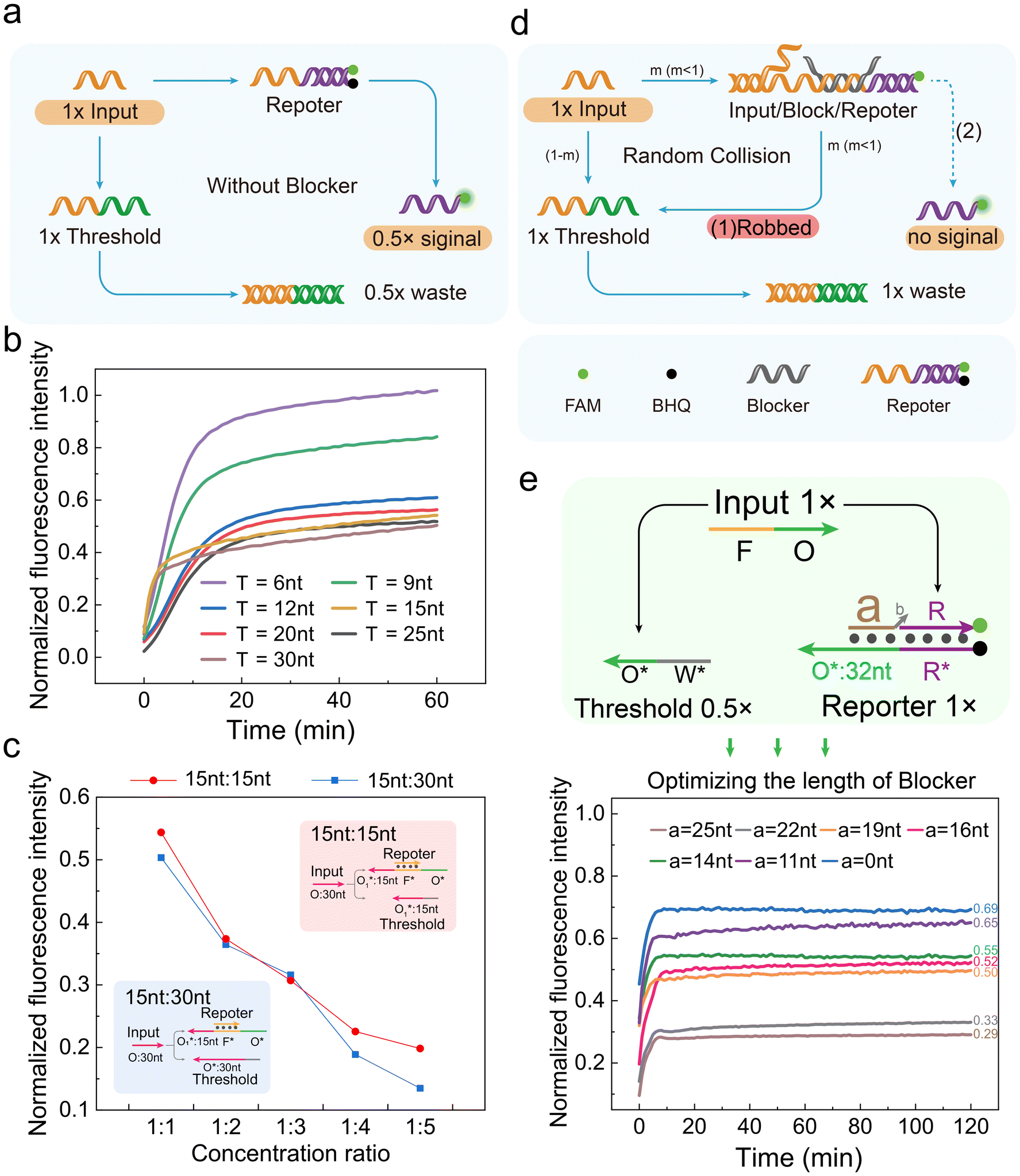 | ||
| Fig. 4 Optimization of the OR gate. (a and d) Intended reaction in the OR gate with or without “blocker”. Without “blocker”, inputs would react with “threshold” and “reporter” randomly and then produced 0.5× leakage. With “blocker”, reaction (2) was much slower than reaction (1); thus, “threshold” could rob inputs from “reporter” and then produce none or little leakage. (b) Kinetics in different length of “threshold” without “blocker”. The number represented matched the length of “threshold” and input. As the threshold length increased, the signal continuously decreases until it stabilized at about 50%. Therefore, length could not make all “threshold” work. (c) Results contrast with different concentrations and lengths of the “threshold” without “blocker”. Ratio “1:5” here means 1× reporter and 5× thresholds, and “1:4” means 1× reporter and 4× thresholds, etc. 15 nt:15 nt means both threshold and “O*” of the reporter were 15 nt, shown in red. 15 nt:30 nt meant that the “O*” of reporter was 15 nt and the threshold was 30 nt, shown in blue. No significant difference was seen here. (e) Kinetics with different lengths of “blocker”. Blocker consisted of sequence “a” and “b”, and “a” was completely matched with “O*”. Individual concentrations and structures of inputs; thresholds and reporters are shown above, and the results are shown below. With different lengths of “a”, the same concentration of thresholds played different roles. The number on the right showed the signal ratio to the positive control. All experiments depicted in the figure were replicated at least three times. | ||
Furthermore, we tried increasing the threshold concentration. The fluorescence signal decreased with increasing threshold concentration, consistent with the reporter:threshold concentration ratio (Fig. 4c and Fig. S7a, S7b†). When the threshold length was 15 nt and the concentration ratio decreased from 1:1 to 1:5, the fluorescence intensity correspondingly decreased from 54% to 19% (red in Fig. 4c). Increasing the Threshold length to 30 nt gave consistent results (blue in Fig. 4c). These results indicated that when the threshold was ≥15 nt, there was little difference between the threshold and reporter in competing for the input. The fluorescence intensity depended only on the concentration. Therefore, length differentiation alone could not enable the threshold to play its role in the OR gate and obtain correct results.
To construct an ideal threshold and achieve correct OR gate logic operations, we introduced the blocker design. As shown in Fig. 4d, the blocker (grey) was first incubated with the reporter. The blocker/reporter binding region partially overlapped the input/reporter binding region. The blocker 3′ end had a 4-base free structure to prevent elongation. After bringing in the blocker, there was a fast, enzyme-driven strand displacement reaction and a slow, enzyme-free strand displacement reaction in the OR gate.
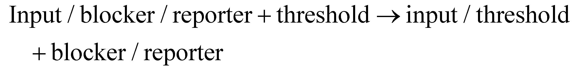 | (1) |
| Input/blocker/reporter → input/reporter + blocker | (2) |
Reactions (1) and (2) correspond to “robbed” and dashed lines in Fig. 4d, respectively. Reaction (1) was enzyme-driven, much faster than the non-enzymatic reaction (2).3,5 Therefore, before depleting the threshold, reaction (1) was the main pathway, making it difficult for the reporter to react with the input. After depleting the threshold, reaction (2) became the main pathway. The input/reporter complex continued react under Bst polymerase action to generate fluorescence signals. The reaction process is shown in Fig. S7c.†
We synthesized a series of blockers of different lengths and tested their performance. As shown in Fig. 4e, the threshold concentration was 0.5×, half the reporter concentration, which makes this operation theoretically correct. When the blocker length was ≤11 nt, blocker/reporter binding was unstable. The final signal generated by 1× input was ∼0.67×, the same as that of no blocker. When the blocker length was ≥22 nt, the enzyme-free strand displacement reaction was insufficient. The final signal generated by 1× input was only 0.3×, indicating significant signal loss. When the blocker length was 14–19 nt, the final signal generated by 1× input was ∼0.5×, indicating that inputs first reacted with the threshold, and when the threshold was depleted, the remaining inputs reacted with the reporter, meeting our expectations. Therefore, the blocker length was determined to be 14–19 nt.
Construction of three-level cascade circuits
Next, we attempted to construct cascade circuits based on the three-level DNA logic gates.First, we tested the AND–OR cascade circuit. The AND gate output was used as an OR gate input, while the rest of the design was consistent with the basic logic gates. The substrate strand, blocker, and reporter system concentrations were all 150 nM. The fuel strand F and threshold concentrations were 450 nM and 50 nM, respectively. Theoretically, when input C is a low-level state, a high-level output can be generated only when both inputs A and B are high-level states. But when C is a high-level state, a high-level output will be generated, regardless of the states of input A and B. As shown in Fig. 5a, the AND–OR cascade circuit returned the correct result for all the input combinations.
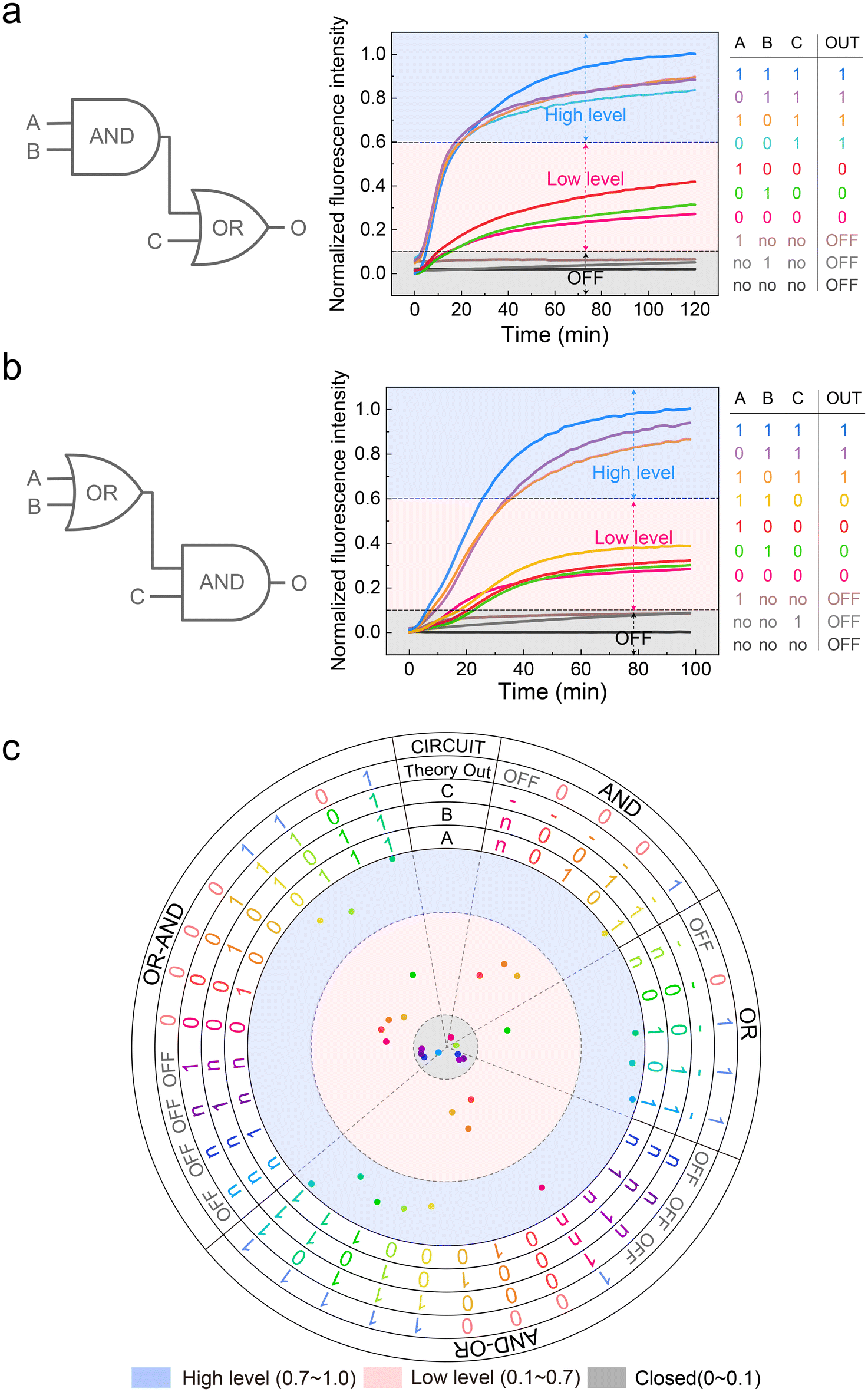 | ||
| Fig. 5 (a and b) Abstraction and kinetics experiments of three-level cascade circuits. The theoretical truth table are listed on the right. Results and truth table were corresponded one by one with the same colour. (c) All the results of basic and cascades circuit. Outermost circle was the type of circuits. “A, B, C” were on behalf of the three inputs, and “n”, “0”, “1” were corresponding to “no”, “50 nM” and “150 nM” of the inputs, respectively. “Theory out” means theoretical output. The actual results are shown at the centre, the same colour as that of the input combinations. Furthermore, the total values were divided into three parts statistically to define the “OFF” (grey), “low level” (red), and “high level” (blue). All the input combinations got the results that matched the truth table. All experiments depicted in the figure were replicated at least three times. | ||
Second, we tested the OR–AND cascade circuit. The OR gate output was used as an AND gate input, while the rest was the same. The concentrations of all the strands were consistent with the AND–OR cascade circuit. Theoretically, when input C is a low-level state, a low-level output is ultimately generated, regardless of the states of input A and B. When input C is a high-level state, a high-level output will be generated whether A or B is a high-level state. As shown in Fig. 5b, the OR AND cascade returned correct results for all the input combinations.
At this point, a total of 34 input combinations, including AND gate, OR gate, and AND–OR, OR–AND cascade circuits have been validated. We summarized all normalized platform values and plotted them as a scatter plot. As shown in Fig. 5c, all the output signals of the OFF state, low-level state, and high-level state fall within a specific area, respectively. To make the three-level concept clearer, we determined separate ranges with different colours, which corresponded to the OFF state (grey), low-level state (red), and high-level state (blue). All the original data and calculation process are provided in the ESI (ESI Files S1 and S2†).
Construction of a three option voting device
The biggest feature of the three-level circuit is distinguishing the OFF state from the logic “0”. Thus, it can recognize three types of inputs: zero, low, and high level. Based on this, we constructed a voting device with three voters and three options. There are usually three situations in real voting scenarios: opposition, abstention, and approval. We corresponded “voter 1”, “voter 2”, and “voter 3” to input A, input B, and input C, respectively, of the circuit. Then, we corresponded the options “opposition”, “abstention”, and “approval” to the zero level (0 nM), low level (50 nM), and high level (150 nM), respectively. We stipulate that when any two out of three agree (150 nM), the output is “approval” (150 nM); when any two out of three abstain (50 nM), exports “abstention” (50 nM); when any two out of three oppose (0 nM), exports “opposition” (0 nM).When we built the voting device using the AND/OR gate components mentioned above, a contradiction arose. Sequence c* of input B needed to match the sequence c of input A, while sequence c* of input C still needed to match the sequence c of input A. In this case, input B and C could not react with each other because they are both sequence c*. To achieve the above functions, we introduced a junction strand (named “J”) in the triplet structure. Two inputs were complementary relying on the J strand, with an 18 nt matching region with the substrate strands (Fig. S8†). Bst DNA polymerase displace the output strand FO, which relied on 3′-OH and the generated signals. The length of the binding region of J and two inputs was 15 nt. The structure of input A and input B was like the basic AND gate, with a length combination of “10 + 2 + 15” and “15 + 2 + 8”, respectively. “10” and “8” were the numbers where the inputs bound to the Substrate strand. “2” was the “–AA–” mismatch at the turning point. The design of input C was different because it needed to react with both input A and input B to generate a signal. Therefore, we extended a sequence at both ends of input C, ultimately forming a length combination of “10 + 2 + 15 + 2 + 8” (Fig. S8†).
To test the voting device, 150 nM of J1, J2, J3, S1, S2, S3, and reporter were pre-added to the system, while 450 nM F strands were also added. As shown in Fig. 6a, under the mediation of the J strand, any two out of three inputs could combine with the corresponding substrate to form the complex and then returned the results (see Fig. S8† for the complexes’ structure). As shown in Fig. 6b, correct results were returned in different combinations of voting situations.
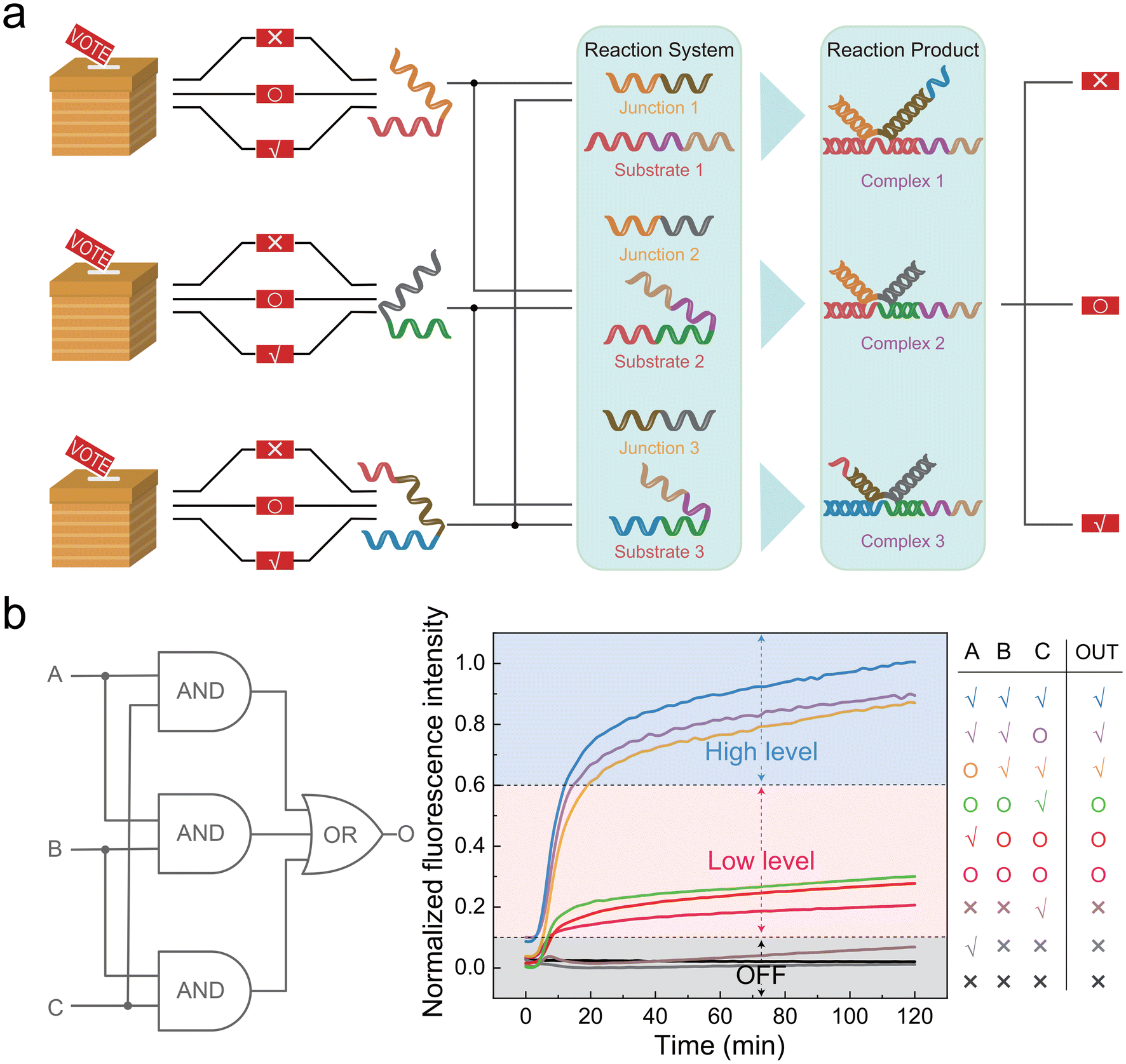 | ||
| Fig. 6 Voting device based on the three-level circuit. (a) Diagram of the voting process. After voting was completed, different concentrations of input were put into the system. “Opposition”, labelled with “×”, was 0 nM; “abstention”, labelled with “○”, was 50 nM; and “approval”, labelled with “√”, was 150 nM. Any two inputs could be cross-linked with one of the substrates to produce complexes. Final output would still be “0 nM”, “50 nM”, “150 nM”, which were the voting results “×”, “○”, “√”. (b) Kinetics experiments of the voting device. All experiments depicted in the figure were replicated at least three times. | ||
Construction of basic/cascade switches
Switch elements based on DNA polymerase have shown great potential in DNA logic circuits. However, there is a design defect, which is that the different binding order between the inputs and the substrate will result in different quantities of outputs. It results in 1× raw material wastage in the system.5 The defect was avoided in our triplet structure.In the switch, the input concentration of 0 nM corresponded to the OFF state, and the input concentration of 100 nM corresponded to the ON state. In a series connection of switches, the circuit was ON only when the inputs were present simultaneously. In a parallel connection of switches, the circuit was ON when either input was in the ON state (ESI Fig. S9†). Subsequently, we conducted a more complex cascade of switches based on series and parallel connection. Still, we got the correct ON/OFF responses with various combinations (ESI Fig. S10†).
Discussion
In this study, we successfully developed a DNA-based three-level logic circuit with unique advantages like low complexity and high flexibility. We implemented basic AND and OR gates and designed and validated cascaded circuits, including AND–OR and OR–AND gates. Furthermore, we used these circuits to construct a voting device with three options and three voters and a switch circuit, further demonstrating the potential of our three-level logic circuit for practical applications.Our three-level logic circuit distinguishes the OFF state from logic “0” by introducing a new low-level state. This innovative design enables our circuits to perform more complex logical operations without increasing the circuit complexity. This is fully reflected in our voting device. Compared to voting devices based on traditional DNA logic circuits, our design achieves higher voting computing power while maintaining the simplicity.15 Looking ahead, the distinction between the OFF state and logic “0” resolves the inherent contradiction of monorail NOT gates, enabling monorail NOT gates.3
The concentration of DNA in practical applications may constrain circuit design initially and further optimization experiments can help ensure functional stability and reliability. Our circuit has not yet been validated in biological systems; future work could explore applying this circuit to biological systems. Although we have demonstrated basic cascaded circuits and an efficient and concise voting device, our design can be further expanded to achieve more complex logical operations.
In summary, our research provides a novel approach to DNA-based logic circuit design. Distinguishing the OFF state from logic “0” by introducing a low-level state, this innovative three-level design enables more complex logical operations without increasing the circuit complexity, as demonstrated in our voting device. Compared to traditional DNA logic circuits, our design achieves higher computing power with lower complexity. Although there are challenges to overcome, our research establishes the foundation for the future optimization and application of this three-level logic circuit. We believe this study provides new insights into designing and applying DNA-based logic circuits and lays the foundation for future research.
Author contributions
The manuscript was written through contributions of all authors. All authors have given approval to the final version of the manuscript. Yuanpeng Zhang and Bei Yan contributed equally.Data availability
The data supporting this article have been included as part of the ESI.† All the raw data will be uploaded later.Conflicts of interest
The authors declare no competing financial interest.Acknowledgements
The authors acknowledge the assistance of Reproductive Health, Tongji Medical College, Huazhong University of Science and Technology. This work was financially supported by the National Natural Science Foundation of China (81871732), the National Key Research and Development Program of China (Grant No. 2021YFC2701402).References
- S. Wang, X. Liu, M. Xu, L. Liu, D. Yang and P. Zhou, Two-dimensional devices and integration towards the silicon lines, Nat. Mater., 2022, 21(11), 1225–1239 CrossRef CAS PubMed.
- L. Ma, X. Song, Y. Yu and Y. Chen, Two-Dimensional Silicene/Silicon Nanosheets: An Emerging Silicon-Composed Nanostructure in Biomedicine, Adv. Mater., 2021, 33(31), e2008226 CrossRef PubMed.
- A. A. Green, P. A. Silver, J. J. Collins and P. Yin, Toehold switches: de-novo-designed regulators of gene expression, Cell, 2014, 159(4), 925–939 Search PubMed.
- L. Qian and E. Winfree, Scaling up digital circuit computation with DNA strand displacement cascades, Science, 2011, 332(6034), 1196–1201 CrossRef CAS PubMed.
- T. Song, A. Eshra and S. Shah, et al., Fast and compact DNA logic circuits based on single-stranded gates using strand-displacing polymerase, Nat. Nanotechnol., 2019, 14(11), 1075–1081 CrossRef CAS.
- D. Y. Zhang and G. Seelig, Dynamic DNA nanotechnology using strand-displacement reactions, Nat. Chem., 2011, 3(2), 103–113 CrossRef CAS.
- T. Fu, Y. Lyu and H. Liu, et al. DNA-Based Dynamic Reaction Networks, Trends Biochem. Sci., 2018, 43(7), 547–560 CrossRef CAS.
- H. Geng, Z. Yin, C. Zhou and C. Guo, Construction of a simple and intelligent DNA-based computing system for multiplexing logic operations, Acta Biomater., 2020, 118, 44–53 CrossRef CAS PubMed.
- F. Wang, H. Lv and Q. Li, et al., Implementing digital computing with DNA-based switching circuits, Nat. Commun., 2020, 11(1), 121 CrossRef CAS.
- C. Xing, X. Zheng and Q. Zhang, Constructing DNA logic circuits based on the toehold preemption mechanism, RSC Adv., 2021, 12(1), 338–345 RSC.
- H. Su, J. Xu, Q. Wang, F. Wang and X. Zhou, High-efficiency and integrable DNA arithmetic and logic system based on strand displacement synthesis, Nat. Commun., 2019, 10(1), 5390 CrossRef.
- W. Li, F. Zhang, H. Yan and Y. Liu, DNA based arithmetic function: a half adder based on DNA strand displacement, Nanoscale, 2016, 8(6), 3775–3784 RSC.
- W. Han and C. Zhou, 8-Bit Adder and Subtractor with Domain Label Based on DNA Strand Displacement, Molecules, 2018, 23(11), 2989 CrossRef PubMed.
- N. Xie, M. Li and Y. Wang, et al., Scaling Up Multi-bit DNA Full Ad-der Circuits with Minimal Strand Displacement Reactions, J. Am. Chem. Soc., 2022, 144(21), 9479–9488 CrossRef CAS PubMed.
- J. Zhu, L. Zhang, S. Dong and E. Wang, Four-way junction-driven DNA strand displacement and its application in building majority logic circuit, ACS Nano, 2013, 7(11), 10211–10217 CrossRef CAS PubMed.
- K. M. Cherry and L. Qian, Scaling up molecular pattern recognition with DNA-based winner-take-all neural networks, Nature, 2018, 559(7714), 370–376 CrossRef CAS.
- M. Wang, C. Tai, W. E and L. Wei, Define: deep convolutional neural networks accurately quantify intensities of transcription factor-DNA binding and facilitate evaluation of functional non-coding variants, Nucleic Acids Res., 2018, 46(11), e69 CrossRef PubMed.
- A. P. Lapteva, N. Sarraf and L. Qian, DNA Strand-Displacement Temporal Logic Circuits, J. Am. Chem. Soc., 2022, 144(27), 12443–12449 CrossRef CAS PubMed.
- A. J. Genot, T. Fujii and Y. Rondelez, Scaling down DNA circuits with competitive neural networks, J. R. Soc., Interface, 2013, 10(85), 20130212 CrossRef , published 2013 Jun 12.
- R. Lopez, R. Wang and G. Seelig, A molecular multi-gene classifier for disease diagnostics, Nat. Chem., 2018, 10(7), 746–754 CrossRef CAS.
- C. Zhang, Y. Zhao and X. Xu, et al., Cancer diagnosis with DNA molecular computation, Nat. Nanotechnol., 2020, 15(8), 709–715 CrossRef CAS PubMed.
- R. Pei, E. Matamoros, M. Liu, D. Stefanovic and M. N. Stojanovic, Train-ing a molecular automaton to play a game, Nat. Nanotechnol., 2010, 5(11), 773–777 CrossRef CAS.
- T. Song, S. Shah and H. Bui, et al., Programming DNA-Based Bio-molecular Reaction Networks on Cancer Cell Membranes, J. Am. Chem. Soc., 2019, 141(42), 16539–16543 CrossRef CAS.
- H. Wang, H. Wang, Q. Wu, M. Liang, X. Liu and F. Wang, A DNAzyme-amplified DNA circuit for highly accurate microRNA detection and intracellular imaging, Chem. Sci., 2019, 10(41), 9597–9604 RSC.
- L. Liu, Q. Hu and W. Zhang, et al., Multifunctional Clip Strand for the Regulation of DNA Strand Displacement and Construction of Com-plex DNA Nanodevices, ACS Nano, 2021, 15(7), 11573–11584 CrossRef CAS.
- Q. Chao, Y. Zhang and Q. Li, et al., Compute-and-Release Logic-Gated DNA Cascade Circuit for Accurate Cancer Cell Imaging, Anal. Chem., 2023, 95(19), 7723–7734 Search PubMed.
- A. T. Glynn, S. R. Davidson and L. Qian, Developmental Self-Assembly of a DNA Ring with Stimulus-Responsive Size and Growth Direction, J. Am. Chem. Soc., 2022, 144(22), 10075–10079 Search PubMed.
- Y. S. Ang, R. Tong and L. Y. Yung, Engineering a robust DNA split proximity circuit with minimized circuit leakage, Nucleic Acids Res., 2016, 44(14), e121 CrossRef.
- Z. A. Zimmers, N. M. Adams and F. R. Haselton, Addition of mirror-image L-DNA elements to DNA amplification circuits to distinguish leakage from target signal, Biosens. Bioelectron., 2021, 188, 113354 CrossRef CAS.
- B. Wang, C. Thachuk, A. D. Ellington, E. Winfree and D. Soloveichik, Effective design principles for leakless strand displacement systems, Proc. Natl. Acad. Sci. U. S. A., 2018, 115(52), E12182–E12191 CAS.
Footnotes |
| † Electronic supplementary information (ESI) available. See DOI: https://doi.org/10.1039/d4nr03606a |
| ‡ These authors contributed equally to this work. |
| This journal is © The Royal Society of Chemistry 2025 |