
A facile approach for fabricating efficient and stable perovskite solar cells
Sajid
Sajid
 ab,
Salem
Alzahmi
*ab,
Nouar
Tabet
c,
Mohammad Y.
Al-Haik
de,
Saleh T.
Mahmoud
f,
Yousef
Haik
gh,
Ahmed Mourtada
Elseman
i and
Ihab M.
Obaidat
*c
ab,
Salem
Alzahmi
*ab,
Nouar
Tabet
c,
Mohammad Y.
Al-Haik
de,
Saleh T.
Mahmoud
f,
Yousef
Haik
gh,
Ahmed Mourtada
Elseman
i and
Ihab M.
Obaidat
*c
aDepartment of Chemical & Petroleum Engineering, United Arab Emirates University, P.O. Box 15551, Al Ain, United Arab Emirates. E-mail: s.alzahmi@uaeu.ac.ae
bNational Water and Energy Center, United Arab Emirates University, P.O. Box 15551, Al Ain, United Arab Emirates
cDepartment of Applied Physics and Astronomy, University of Sharjah, P.O. Box 27272, United Arab Emirates. E-mail: iobaidat@sharjah.ac.ae
dDepartment of Sustainable and Renewable Energy Engineering, University of Sharjah, Sharjah, 27272, United Arab Emirates
eDepartment of Mechanical Engineering, Higher Colleges of Technology, 25035, Abu Dhabi, United Arab Emirates
fDepartment of Physics, United Arab Emirates University, P.O. Box 15551, Al Ain, United Arab Emirates
gDepartment of Mechanical and Nuclear Engineering, University of Sharjah, Sharjah, United Arab Emirates
hDepartment of Mechanical Engineering, The University of Jordan, Amman, Jordan
iCentral Metallurgical Research & Development Institute (CMRDI), Cairo, Egypt
First published on 7th November 2024
Abstract
Perovskite solar cells (PSCs) with high power conversion efficiencies (PCEs) can be produced using a variety of methods, such as different fabrication methods, device layout modification, and component and interface engineering. The efficiency of a perovskite solar cell is largely dependent on the overall quality of the perovskite thin-film in every scenario. The utilization of spin-coating followed by the antisolvent pouring (ASP) method is prevalent in nearly all fabrication techniques to achieve superior perovskite thin-films. Nevertheless, there are a few guidelines that must be followed precisely when using the ASP approach, including the antisolvent amount, duration, and area for dropping. The aforementioned challenging and necessary strategies frequently result in perovskite thin-films with pinholes, tiny grains, and broad grain boundaries, which impair the performance of PSCs. Therefore, the implementation of a straightforward approach that does not require the use of such complex ASP steps is crucial. Here, we employ a simple process that involves the hot-dipping of lead iodide (PbI2) thin-films in a hot solution of methylammonium iodide (MAI) and formamidinium iodide (FAI) in isopropanol (IPA) to produce high-quality perovskite thin-films. As the time required for the desired perovskite to crystallize is critical, we carefully examined various hot-dipping process times, such as 10 seconds, 20 seconds, 30 seconds, and 40 seconds. These time intervals yielded thin-films, which were named PSK-10, PSK-20, PSK-30, and PSK-40, respectively. Morphological and optoelectronic characterization demonstrated the high quality of the perovskite thin-films obtained through dipping PbI2 for 30 seconds. Consequently, the PSK-30-based PSCs produced higher PCEs of up to 21.52% compared to those of the ASP-based devices (20.79%). Furthermore, the unsealed PSCs prepared with PSK-30 and ASP were assessed for 252 hours at 25 °C and 40–45% relative humidity in order to determine their operational stability. The ASP-based device showed poor stability, retaining only 10% of its original PCE, whereas the PSK-30-based device retained 70% of its initial PCE. These results offer a new and viable approach for producing highly efficient and stable PSCs.
Introduction
Owing to their low production costs and high power conversion efficiencies (PCEs), perovskite solar cells (PSCs) are drawing more interest from scientists.1 The exceptional optoelectronic characteristics of perovskites, including their long diffusion length, high absorption coefficient, high defect tolerance, and long exciton lifespan, are a result of their distinct nanostructures.2 Over the past few decades, there has been a notable increase in PSC efficiency over 26% thanks to advancements in both device modification and materials science.3–7 Perovskite thin-films are the most vital components of PSCs, as is widely known.8,9 In PSCs, for instance, it has been realized that trap states generated by pinholes, crystal defects, and grain boundaries result in charge-carrier recombination.10,11 Moreover, recombination of charges and moisture intrusion are often enhanced by open regions at grain boundaries and interfaces, which decrease the PSC stability and performance.12 Larger grains and fewer grain boundaries in perovskite thin-films can aid in reducing trap states and charge recombination. Grain size and crystal growth rate modulation are still vital to produce uniform, pinhole-free perovskite thin-films with minimal grain boundaries.13 Numerous methods have been demonstrated in this context to fabricate perovskite thin-films with large grains and minimum trap states. To produce micro-sized grains, Li et al.,14 for instance, introduced additives to perovskites. Xu et al.15 reported that large-grain perovskite thin-films can be obtained through the inhibition of heterogeneous nucleation. In addition, a combination of antisolvent vapour-assisted and space-confinement crystallization techniques has been used to produce millimeter-sized thin mono-crystals of perovskites with excellent quality.16,17 High-quality perovskite thin-films can also be produced by spin-coating, chemical/physical vapour deposition, and chemical bath deposition.18One of most popular techniques for fabricating high-quality perovskite thin-films is spin-coating followed by antisolvent pouring (ASP). However, there are undoubtedly some difficulties with the ASP procedure.19 For example, because perovskite thin-films form quickly, there is a very small window of time during spin-coating. Therefore, the antisolvent needs to be precisely poured a few seconds after the substrate rotates or before the spinning process stops. Moreover, several other factors, such as the specific speed of spin-coating, the quantity of antisolvent, the distance of dropping of the antisolvent, and the area where the antisolvent needs to be poured, have a major impact on the quality of perovskite thin-films and, in turn, the performance of the resulting PSCs.20 This implies that expert researchers could handle the ASP method required to produce high-quality perovskite thin-films. Consequently, a facile process is required for fabricating desirable perovskite thin-films in PSCs without the need for complicated ASP management. Our main goal in this work is to fabricate perovskite thin-films without using the spin-coating and antisolvent processes. In addition, when compared to two-step methods,21,22 hot-dipping is less complex and more straightforward to follow. Immersion in the hot precursor allows for better control over film uniformity than the two-step process of spin-coating, heating, and processing precursor solutions independently. The hot-dipping process may result in fewer defects in the perovskite film. This is because the process can promote more even and complete substrate coverage, which reduces the likelihood of issues like pinholes and irregularities that could occur with the two-step method. Moreover, hot-dipping can operate at lower temperatures than the high-temperature annealing frequently required in the two-step process. The hot-dipping method can be useful when trying to reduce energy consumption or for substrates that are temperature sensitive.
Here, we demonstrate a facile approach, which involves the hot-dipping of PbI2 substrates in FAI/MAI hot precursor solution. A 30-second hot-dipping process was found to produce a perovskite thin-film with large grains and a smooth pinhole-free surface after examining the hot-dipping process for different durations. Without employing the challenging ASP method, the PSK-30-based PSC showed a highest PCE of 21.52%, while the PSC prepared with the ASP method showed a highest PCE of 20.79%. The long-term operational stability of the unsealed PSCs was tested for 252 hours under ambient conditions at 25 °C and 40–45% relative humidity. The efficiency of the PSK-30-based device decreased by only 30%. On the other hand, the ASP-based device lost 90% of its PCE and exhibited significant degradation and poor stability. The PCE of the PSK-30-based PSC remains at 20.01% when tracking the maximum power point at 0.95 V and 25 °C for 3000 minutes of continuous illumination, while the ASP-based device's efficiency decreases to 0.94%.
Results and discussion
While the ASP method is widely used to prepare high-quality perovskite thin-films, a few related issues need to be dealt with. These include the area over which the antisolvent should be poured, the antisolvent dripping time window, and the dripping distance. As shown in Fig. 1, we address these issues by introducing the dipping of PbI2-coated hot substrates in a hot precursor solution of MAI and FAI in IPA. Moreover, a direct formation mechanism is put forth using the nucleation growth theory framework.23 Consequently, the phase change is driven by a hot precursor solution and a hot substrate, leading to an ultrashort crystallization process.24 Meanwhile, adequate thermal energy makes it easier for atoms to diffuse throughout a liquid without creating an intermediate phase. In order to obtain high-quality perovskite thin-films with notable benefits including rapid crystallization, a short film formation process, a large increase in the grain size, preferred crystalline orientation, and low defect states, the hot-PbI2 substrate is dipped in a hot MAI/FAI solution. Previously, nucleation growth has been shown to be significantly influenced by the hot precursor solution, substrate temperature, and thermal annealing. The process of perovskite film formation can be split into three stages when the temperatures of the substrate and precursor solutions are below 100 °C: the initial solution stage, the transition-to-solid film stage, and the transformation stage from intermediates to a perovskite film.25 On the other hand, in our work, a direct formation mechanism is used to form the perovskite film when the temperatures of the precursor solution and the substrate are raised.23 The duration of the PbI2 substrates’ immersion in the MAI and FAI solutions is thought to be crucial for producing the desirable perovskite thin-films.26 Consequently, compared to the ASP method, the hot-dipping approach does not require significant effort to achieve ideal conditions for the fabrication of high-quality perovskite thin-films.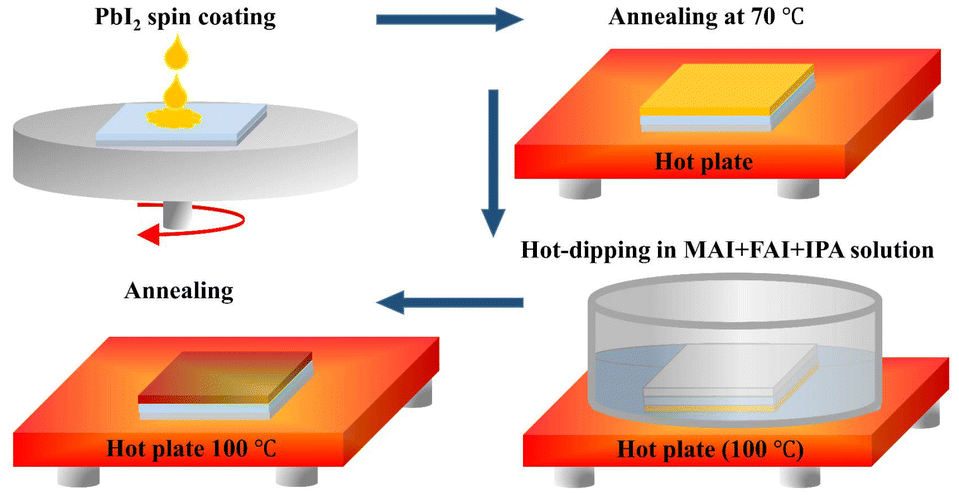 | ||
| Fig. 1 Schematic illustration of the PbI2 hot-dipping in MAI/FAI/IPA solution. | ||
The PbI2 thin-films were initially produced by spin-coating PbI2 solution in dimethylformamide (DMF) and dimethyl sulfoxide (DMSO), as shown in Fig. 1. Previous studies have shown that the defect/trap states in the perovskite layers are produced by small grains with multiple grain boundaries and pinholes.27,28 Subsequent investigations revealed that the luminescence peak is significantly stronger in the perovskite grain centers than it is near the grain boundaries, suggesting that trap-assisted recombination is responsible for the increased charge recombination at the grain boundaries.29 Since the dipping process during nucleation and crystal formation of the desirable perovskite affects the size and boundaries of the perovskite's grains, as illustrated in Fig. 2 and 3, we used scanning electron microscopy (SEM) and atomic force microscopy (AFM) to examine the surface morphologies of the obtained perovskite thin-films. The morphological SEM images of the final PbI2 thin-films are displayed in Fig. 2(a and b).
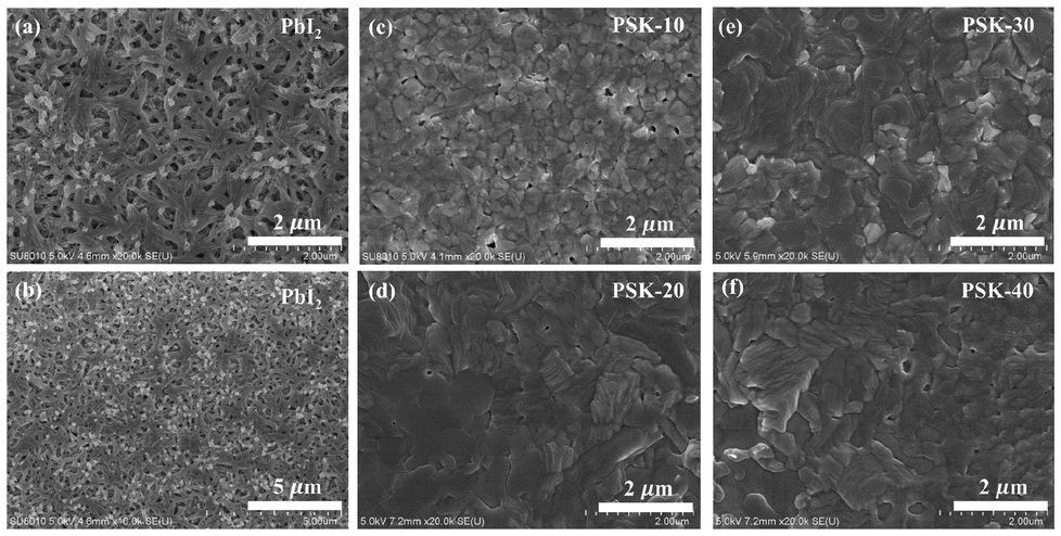 | ||
| Fig. 2 SEM images of the PbI2 thin-films (a and b) and perovskite thin-films fabricated with hot-dipping of the as-prepared PbI2 thin-films for 10 seconds (c), 20 seconds (d), 30 seconds (e), and 40 seconds (f). | ||
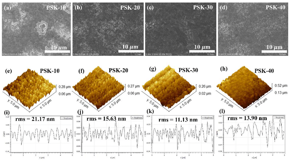 | ||
| Fig. 3 Surface SEM images (a–d) and AFM images (e–h) of the perovskite thin-films and (i–l) surface roughness values of the perovskite thin-films fabricated with hot-dipping of the PbI2 thin-films for 10 seconds, 20 seconds, 30 seconds, and 40 seconds, respectively. | ||
Compared to the dipping of the hot PbI2 substrate in the hot MAI and FAI precursor solution for 10, 20, or 40 seconds (labeled as PSK-10, PSK-20, and PSK-40), as shown in Fig. 2(c–f), and 3, a 30-second dipping process (labeled as PSK-30) produced a relatively dense perovskite thin-film with large grains, few grain boundaries, and full coverage without pinholes.
The device performance is significantly hampered by the remaining PbI2 on the formed film's surface. The PbI2 at the corresponding interface is responsible for the catalytic site that can lead to perovskite degradation during device operation.30 Meanwhile, unreacted residual PbI2 is more likely to form Pb0-rich voids,30,31 which serve as sites for nonradiative recombination in PSCs. In this context, it is desirable to obtain a perovskite thin-film without residual PbI2. As some residual PbI2 can be seen in the large-scale SEM images in Fig. 3(a, b, and d), it was found that the short dipping period is insufficient to produce the desired perovskite thin-films, leading to an unconverted PbI2 phase.32,33 Furthermore, residual PbI2 arose from a prolonged dipping time. On the other hand, the 30-second (Fig. 3(c)) dipping process showed the desired perovskite thin-films free of any remaining PbI2 phase. When compared to the thin-films fabricated using the 10-second, 20-second, and 40-second dipping processes, it is evident that the perovskite films produced by the 30-second dipping process are uniform, smooth and fully covered, in addition to having large grains with small boundaries. The root-mean-square (rms) values in Fig. 3(e–l) demonstrate how using the 30-second dipping process significantly improved the smoothness of the as-prepared perovskite films. The rms value is decreased from 21.17 nm to 11.13 nm as can be seen in Fig. 3(e–l). The lower roughness obtained for the PSK-30-based perovskite film is beneficial for charge transport within the film and across the interface at the perovskite/charge transport layer.34
Phase changes in the unreacted PbI2 could have an impact on the stability and efficiency of the solar cell. For best results, the desired crystalline structure must be maintained.31 In this regard, XRD was used to analyze the crystallinity of the resulting perovskite thin-films, as shown in Fig. 4 and 5. The (110) and (220) planes at 14° and 28° in the XRD pattern of the PSK-30-based perovskite thin-film can be indexed to the pure phase of the perovskite, as reported previously.32 The peaks of unreacted PbI2 disappeared as shown in Fig. 4(c) and 5(c), demonstrating the formation of a higher quality perovskite thin-film.
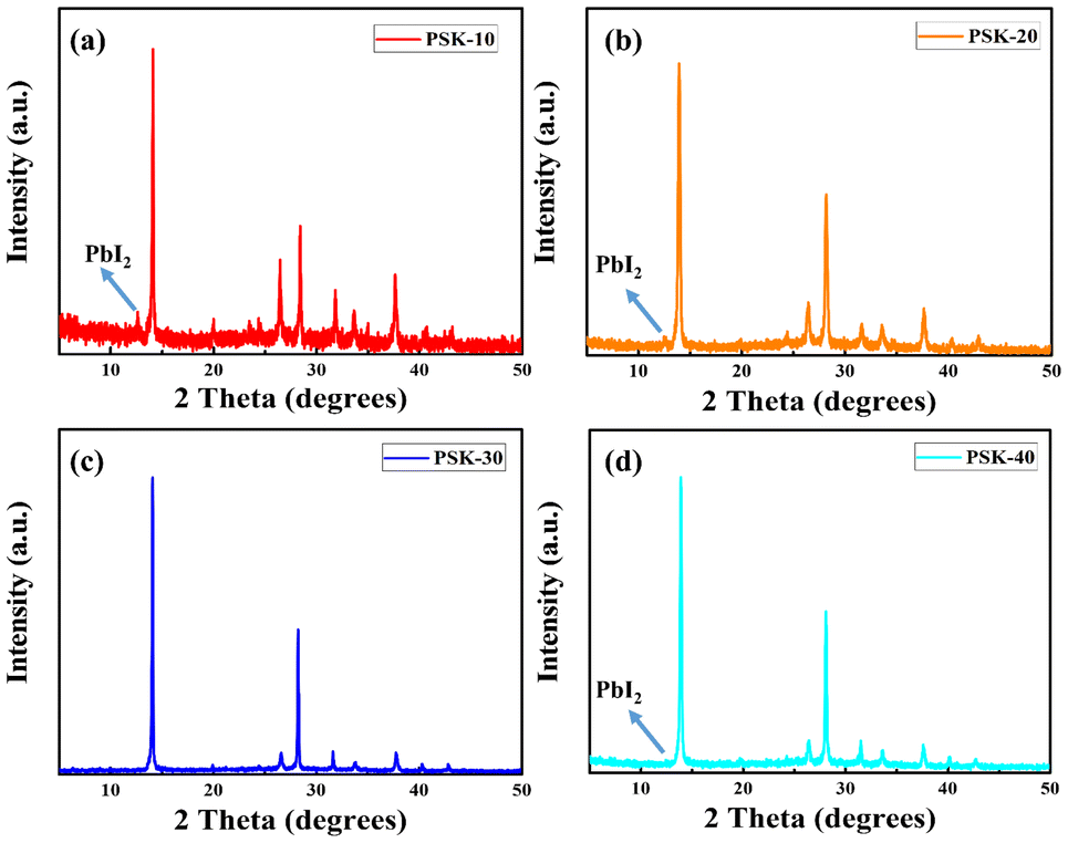 | ||
| Fig. 4 X-rays diffraction peaks of the perovskite thin-films obtained through hot-dipping of PbI2 for (a) 10 seconds, (b) 20 seconds, (c) 30 seconds, and (d) 40 seconds, respectively. | ||
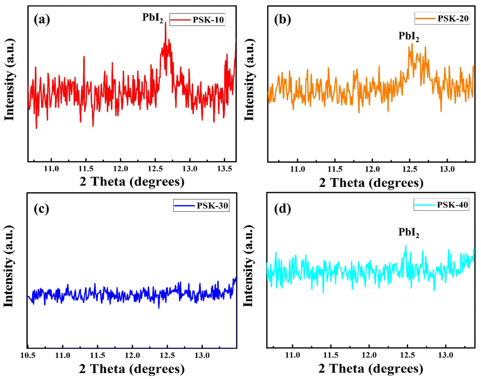 | ||
| Fig. 5 Zoomed-in X-ray diffraction patterns for the residual PbI2 in the final thin-films fabricated with hot-dipping of the PbI2 thin-films for 10 seconds (a), 20 seconds (b), 30 seconds (c), and 40 seconds (d), respectively. | ||
However, as shown in Fig. 4 and 5, the intensities of the (001) peaks of PbI2 show an increase in the number of cases of PSK-10, PSK-20, and PSK-40, indicating residual PbI2. Therefore, dipping the PbI2 substrates for a short or long time is not suitable to produce the desired perovskite thin-films.
Utilizing ultraviolet-visible (UV-vis) absorption spectroscopy, steady-state photoluminescence (PL), and time-resolved photoluminescence (TRPL), the optoelectronic characteristics of the resulting perovskite thin-films were examined. As PSK-30 absorbs more light than PSK-10, PSK-20, and PSK-40 do, Fig. 6(a) indicates a low density of in-gap imperfections.35 This is beneficial because it allows for the photogeneration of more electron–hole pairs, which leads to the enhancement of cell performance.36 Furthermore, we expect larger absorption of light when the substrate is coated with a film with large grain size without pinholes, as in the case of PSK-30.37Fig. 6(b) shows the PL spectra of the as-prepared perovskite thin-films that were deposited on top of the glass substrates. Peak emission at nearly 770 nm was noticed in all perovskite thin-films.
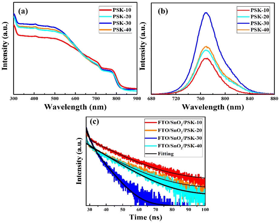 | ||
| Fig. 6 Optoelectronic characterization of the as-prepared perovskite thin-films: UV-vis absorption spectra (a), PL spectra (b) and TRPL spectra (c). | ||
It is well known that a sharp, highly intense PL peak is observed when the perovskite layer is deposited on a glass substrate; this indicates the good quality of the films that leads to a lower carrier recombination via non-radiative defect-assisted processes. The bound excitons can remain in the perovskite film for a longer time before they are separated into free electrons and holes. The intensity of the PSK-30 peak has significantly increased as compared to those of the PSK-10, PSK-20, and PSK-40 peaks, as indicated by PL spectroscopy, suggesting that the 30-second hot-dipping process of PbI2 in the hot solution of MAI/FAI reduces the bulk/surface defects and trap-induced charge-carrier recombination.38
We utilized TRPL spectroscopy (Fig. 6(c)) to obtain a deeper comprehension of the charge-carrier extraction/recombination dynamics at the interface of the FTO/SnO2/perovskite. The average PL lifetime of the FTO/SnO2/PSK-30 film (2.66 ns) is less than those of the FTO/SnO2/PSK-10, FTO/SnO2/PSK-20, and FTO/SnO2/PSK-40 films, as listed in Table 1, based on the fitting of TRPL decay with a bi-exponential function.39 The TRPL findings indicate that PSK-30 exhibits a significantly faster decay of the TRPL signal. This can be assigned to the higher extraction rate of electrons at the perovskite/SnO2 interface as previously reported.40 The increase of the bulk carrier lifetime due to the reduction of Shockley–Read–Hall (SRH) recombination in the perovskite film enables a larger fraction of electrons to reach the interface with SnO2.41
| Sample | τ1 (ns) | τ2 (ns) | 〈τ〉 (ns) |
|---|---|---|---|
| FTO/SnO2/PSK-10 | 0.927 | 10.01 | 5.47 |
| FTO/SnO2/PSK-20 | 0.424 | 9.40 | 4.91 |
| FTO/SnO2/PSK-30 | 1.173 | 4.15 | 2.66 |
| FTO/SnO2/PSK-40 | 0.931 | 8.18 | 4.55 |
Considering the previously mentioned properties of the as-prepared perovskite thin-films, we fabricated solar cells with stack layers of FTO/SnO2/perovskite/Spiro-OMeTAD/Au using the ASP and PbI2 hot-dipping approach for 30 seconds. A high photovoltaic output is expected since more excitons can be separated into free holes and electrons. The surface morphologies of the ASP- and PSK-30-based perovskite thin-films fabricated on FTO/SnO2-substrates are presented in Fig. 7. The cross-sectional SEM images and current–voltage (J–V) characteristic curves of the as-fabricated devices are shown in Fig. 8(a–d).
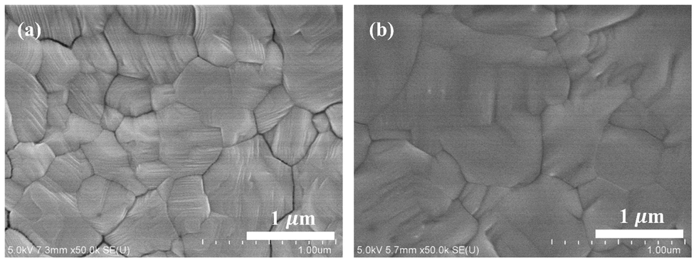 | ||
| Fig. 7 Surface SEM images of the perovskite thin-films prepared with ASP (a) and PbI2 hot-dipping (b). | ||
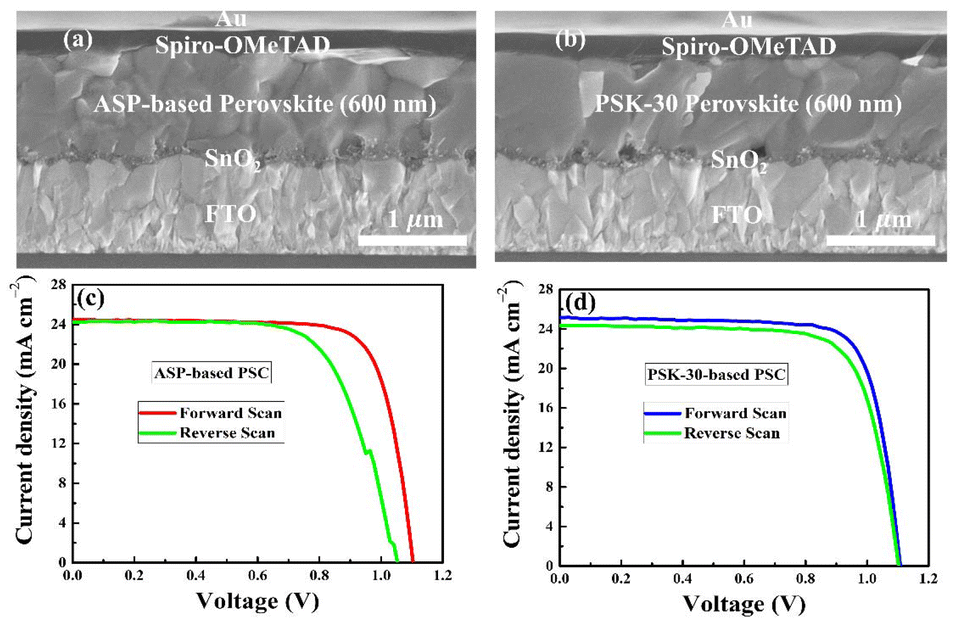 | ||
| Fig. 8 Cross-sectional SEM images (a and b) and J–V characteristic curves under forward and reverse scans (c and d) of the PSCs prepared with the ASP step and PbI2 hot-dipping. | ||
With the forward-biased voltage, the ASP-based PSCs provide a maximum PCE of 20.79% (Fig. 8(c)). Fig. 8(d) displays the J–V curves of the PSK-30-based PSCs. Under the same experimental conditions, the PCE increases to 21.52%. The short-circuit currents (Jsc) and PCEs of the PSK-30-based PSCs are higher than those of the PSCs fabricated with the SAP step, as shown in Table 2. From 24.47 mA cm−2 to 25.13 mA cm−2, the Jsc increases. High Jsc and PCE are believed to be caused by the perovskite thin-film's superior light harvesting and compact large grains with minimum grain boundaries, as can be seen in Fig. 7. To confirm the reliability of the PSCs, their hysteresis phenomena were examined. There has been speculation that charge trapping and ion migration are responsible for the most frequent hysteric phenomena in PSCs.42,43 All the devices exhibit hysteresis (Fig. 8(c and d)); the ASP-based PSCs have more hysteresis compared to the PSK-30-based PSCs. The estimated PCE variance for a PSK-30-based PSC is 1.54%, whereas the value is 3.5% for an ASP-based device. The smaller hysteresis effect in the devices can be explained by the reduced charge-carrier trapping at the grain boundaries of the PSK-30-based thin-films. The gaps between the grains of the ASP-based perovskite layer will trap free charges or ions, leading to severe recombination and a significant loss of the PCE.44 On the other hand, the PSK-30-based perovskite layer has fewer grain boundaries, which facilitates charges passing through the crystals more efficiently and decreases the hysteresis effect in the PSCs.
| PSC based on | V oc (V) | J sc (mA cm−2) | FF (%) | Eff. (%) | Scan |
|---|---|---|---|---|---|
| ASP | 1.109 | 24.47 | 76.60 | 20.79 | Forward |
| — | 1.057 | 24.20 | 67.58 | 17.29 | Reverse |
| PSK-30 | 1.109 | 25.13 | 77.21 | 21.52 | Forward |
| — | 1.107 | 24.34 | 74.00 | 19.98 | Reverse |
Fig. 9(a) displays the external quantum efficiencies (EQEs) of the PSK-30- and ASP-based PSCs. For the ASP-based PSC, the integrated Jsc is 22.97 mA cm−2, whereas for the PSK-30-based device, the integrated Jsc is 24.02 mA cm−2. According to Saliba et al.,45 the integrated Jsc values are normally not certified and are primarily obtained in the relevant laboratories. As per their report, the integrated Jsc value frequently falls between 10 and 20% of the Jsc value obtained from the J–V curves. As a result, for PSCs, the Jsc value derived from the J–V curve is frequently greater than the integrated Jsc value from the EQE. This implies that our measurement from the J–V curve is reasonably precise, suggesting that the integrated Jsc values roughly agree with the Jsc values obtained from the J–V curves. The recombination resistance (Rr) of the as-prepared PSCs under photoexcitation at a reverse bias voltage of 0.9 V in the frequency range of 1 Hz to 1 MHz was measured using electrical impedance spectroscopy (EIS), as indicated by the Nyquist plots in Fig. 9(b) with an equivalent circuit. The signature of the recombination resistance is known to be at low frequencies (Rr), while the high-frequency portion of the EIS analysis is thought to represent the transfer resistance (Rt). Since the electron- and hole-transporting layers remain the same across all devices, we believe that the perovskite layer is the only component that influences the Rt and Rr. The ASP-based PSC shows an Rt value of 8.18 Ω and an Rr value of 77.39 Ω, whereas the PSK-30-based device exhibits the largest Rr value of 94.63 Ω and the smallest Rt value of 3.40 Ω based on the numerical fitting. In accordance with the previously mentioned observations, the large Rr value efficiently prevents the recombination of charges, while the small Rt value is advantageous for charge extraction.44,46–48
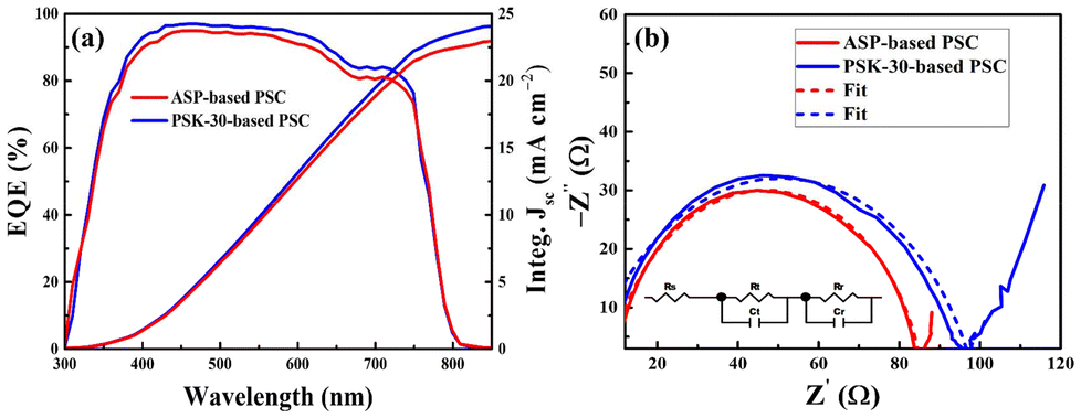 | ||
| Fig. 9 External quantum efficiencies (a) and electrical impedance spectra (b) of the ASP- and PSK-30-based PSCs. | ||
Meanwhile, an investigation was performed on the repeatability of the PSK-30- and ASP-based PSCs (across 8 devices for each). Comparing the PSK-30-based PSCs to the ASP-based PSCs—specifically the Jsc, FF, and PCE—Fig. 10 demonstrates a significant increase in PSC performance and reproducibility. For eight PSCs based on ASP, the Jsc, FF, and PCE parameters were widely distributed. However, for the PSK-30-based PSCs, the Jsc, FF, and PCE values were all within a narrow range, demonstrating the significance of hot-dipping in obtaining large and high-quality perovskite thin-film grains for high photovoltaic performance of the device.
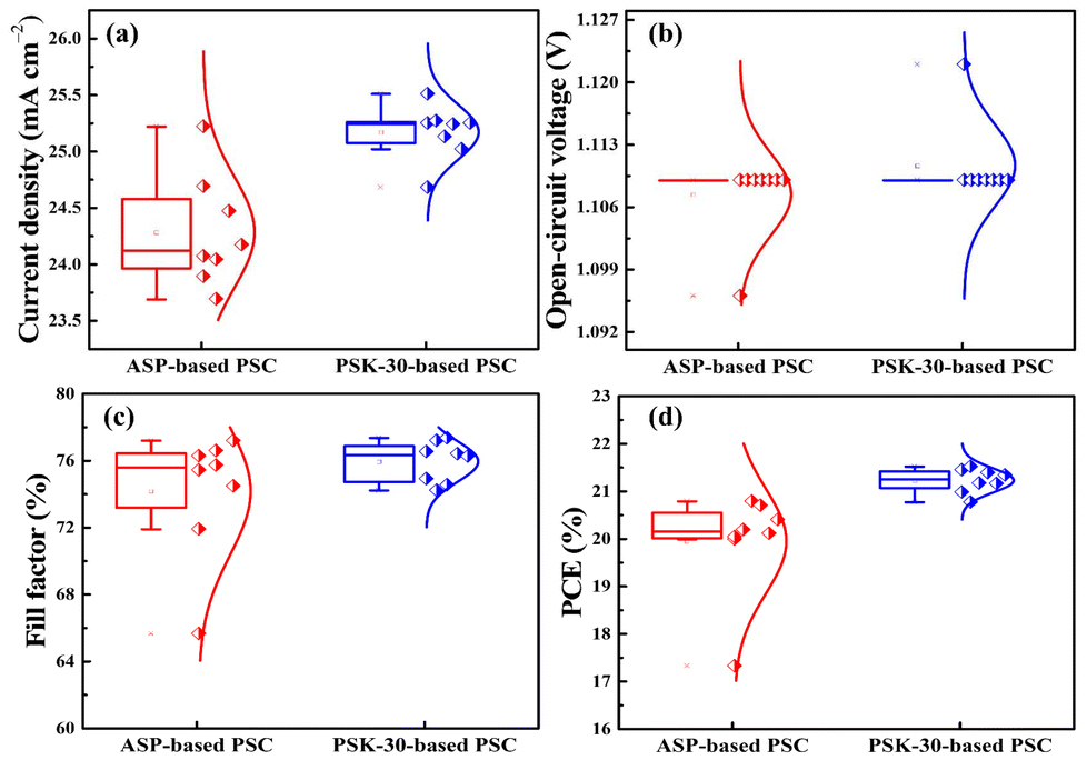 | ||
| Fig. 10 Statistical data of the as-prepared PSCs with the ASP and PSK-30 thin-films (a) Current-density, (b) Open-circuit voltage, (c) Fill factor, and (d) Power conversion efficiency. | ||
Long-term stability, especially operational stability in ambient air, is another essential requirement for PSCs in addition to considerable PCE. The unsealed PSCs were subjected to a 252-hour test at 25 °C and 40–45% relative humidity, as shown in Fig. 11(a). The PSK-30-based device's efficiency only decreased by 30% after continuous operational assessment; it retained 70% of its initial PCE. On the other hand, the PCE of the ASP-based device showed severe degradation and poor stability, losing 90% of its efficiency and retaining only 10% of the original PCE. In addition, performance of the as-prepared devices was evaluated in tracking the maximum power point at 0.95 V and 25 °C under AM 1.5G illumination in an ambient environment. After 3000 minutes of continuous illumination, the PSK-30-based PSC outperforms the ASP-based device, as can be seen in Fig. 11(b). After continuous illumination, the PCE of the PSK-30-based PSC remains at 20.01%, while the ASP-based device's efficiency drops to 0.94%. The significant interconnected large grains with minimal boundaries are what give PSK-30-based PSCs their long-term stability. However, the ASP-based device experiences moisture penetration more quickly because the perovskite thin-films produced by this method have many gaps between grain boundaries and a notably small grain size,16 Moreover, compared to smaller grains, larger grains have fewer grain boundaries. Because grain boundaries frequently have dislocations and other flaws that can cause degradation, they can serve as sites for defects and instability. Larger grains can also reduce the material's total surface energy. Higher surface-to-volume ratios in smaller grains can lead to increased reactivity and susceptibility to environmental factors like moisture. These findings suggest that the PSK-30-based solar cells will likely be more stable over time than the ASP-based devices.
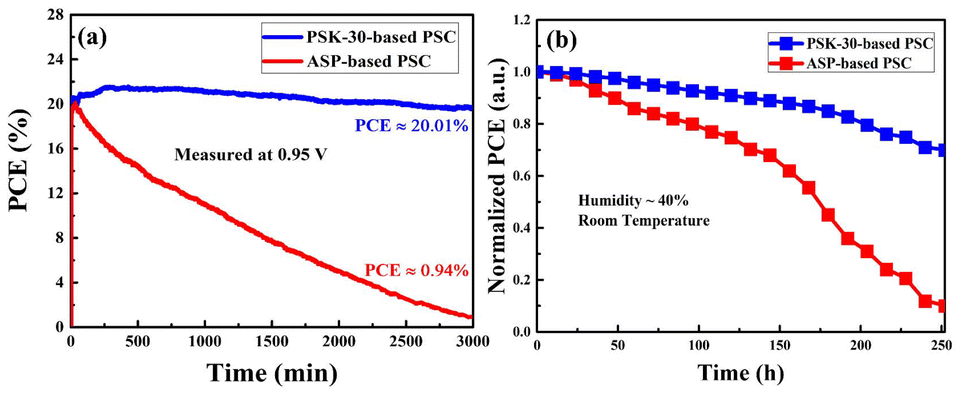 | ||
| Fig. 11 Stability of the unencapsulated PSCs at maximum power point tracking at 0.95 V and 25 °C under continuous AM 1.5G illumination in an ambient environment (a). Long-term stability of the unencapsulated PSCs at room temperature under AM 1.5G illumination with a relative humidity of 40–45% (b). | ||
Conclusion
We present a simple hot-dipping technique that produces high-quality perovskite thin-films without the need for challenging traditional spin-coating and antisolvent dripping procedures (ASP). It is not necessary to exert significant effort when using the hot-dipping strategy to determine the optimal conditions for producing perovskite thin-films of high quality. In contrast to designs that relied on ASP, the PCEs of the hot-dipping-based PSCs increased from 20.79% to 21.52%. In addition, after the unsealed devices were tested for 252 hours at 25 °C and 40–45% relative humidity, the PSK-30-based PSC showed better stability than the ASP-based device. The large grain size with fewer grain boundaries, pinhole-free morphology, and high crystallinity are all responsible for the improved performance. Reduced moisture intrusion and improved charge-carrier transport and collection are the results of these characteristics. This work offers a viable route toward the development of high-quality perovskite thin-films, which may lead to excellent perovskite-based photovoltaic performance.Materials and methods
Precursor solution
To make the SnO2 solution, 133 μl of colloidal SnO2 solution was diluted with 866 μl of deionized water. In anhydrous dimethylformamide/dimethyl sulfoxide solution (900 μl/100 μl), 691.5 mg of lead iodide (PbI2) was dissolved for the purpose of hot-dipping. 2 ml of isopropanol was used to dissolve 12.8 mg of methylammonium iodide (MAI) and 180 mg of formamidinium iodide (FAI). Anhydrous dimethylformamide/dimethyl sulfoxide solution was mixed (9![[thin space (1/6-em)]](https://www.rsc.org/images/entities/char_2009.gif) :1) to dissolve 6.4 mg of MAI, 90 mg of FAI, and 691.5 mg of PbI2 in order to prepare the perovskite precursor solution for spin-coating. The final FAMAPbI3 perovskite thin-films were obtained after hot-dipping and spin-coating. The precursor solution of Spiro-OMeTAD was prepared at a concentration of 72.3 mg ml−1 in chlorobenzene. 26.6 μl of tert-butylpyridine and 17.5 μl of lithium bis-(trifluoromethanesulfonyl)-imide were added, and the mixture was stirred for six hours in a glove box.
:1) to dissolve 6.4 mg of MAI, 90 mg of FAI, and 691.5 mg of PbI2 in order to prepare the perovskite precursor solution for spin-coating. The final FAMAPbI3 perovskite thin-films were obtained after hot-dipping and spin-coating. The precursor solution of Spiro-OMeTAD was prepared at a concentration of 72.3 mg ml−1 in chlorobenzene. 26.6 μl of tert-butylpyridine and 17.5 μl of lithium bis-(trifluoromethanesulfonyl)-imide were added, and the mixture was stirred for six hours in a glove box.
Device fabrication
For a duration of 20 minutes, the FTO substrates were sequentially sonicated in deionized water, acetone, and isopropyl alcohol. The substrates were subjected to a 15-minute UV ozone treatment after being further dried by blowing nitrogen. The SnO2 solution was spin-coated for 15 seconds at 3000 rpm on the cleaned FTO substrates, and then annealed for 30 minutes at 150 °C. Following a 15-minute UV ozone treatment and cooling to room temperature, the FTO/SnO2 substrates were then transferred to a glove box. PbI2 hot-dipping in MAI and FAI hot solution and spin-coating followed by antisolvent dripping were the two techniques utilized for making the perovskite thin-films. The perovskite precursor was prepared as described and spin-coated on an FTO/SnO2 substrate for 30 seconds at 4000 rpm. The spin-coating process was followed by an antisolvent dripping technique. The substrates were exposed to 600 μl of chlorobenzene for 15 seconds prior to the end of spin-coating. In order to prepare the PbI2 thin-film for hot-dipping, the PbI2 solution was spin-coated on the FTO/SnO2 substrate for 30 seconds at 1500 rpm, and it was then annealed for 1 minute at 70 °C. The hot PbI2 substrates were placed in a Petri dish with a hot solution (100 °C) of MAI and FAI. PbI2 was hot-dipped for 10, 20, and 30 seconds, respectively. The as-prepared substrates were heated for 10 minutes at 100 °C and allowed to cool to room temperature naturally. Both the SAP- and hot-dipping-based perovskite thin-films were spin-coated with Spiro-OMeTAD solution at 4000 rpm for 30 seconds. Finally, 80 nm gold electrodes were evaporated on the as-prepared films to complete the solar cells. A metal mask was used in all devices to obtain a 0.1 cm2 active area.Characterization
A scanning electron microscope (Hitachi S-4800) and an atomic force microscope (Aglient Keysight, AFM-5500) were used to investigate the morphologies of the as-prepared perovskite films. XRD (Bruker D8 Advance X-ray diffractometer, Cu-Kα radiation λ = 0.15406 nm) was used to study the chemical composition and crystal structure of the perovskite. A UV-vis spectrophotometer (UV-2600) was used to record the absorption spectrum. The steady PL spectra of the as-prepared perovskite films were analyzed using an Edinburg PLS 980. The TRPL decay of the perovskite films was measured using a transient state spectrophotometer (Edinburg Ins. F900) under a 485 nm laser. The current–voltage curves were obtained with a source meter (Keithley 2400) using forward (−0.1–1.2 V) scans from a solar simulator (XES-301S+EL-100) under AM 1.5G irradiation with a power intensity of 100 mW cm−2. The step voltage was set to 12 mV and the delay time was set to 10 ms. QE-R systems (Enli Tech.) were used to determine the EQE. An electrochemical workstation (Zahner Zennium) was used to perform the EIS measurement.Author contributions
Conceptualization: S. S., I. M. O., A. M. E., and S. A.; supervision and validation: I. M. O. and S. A.; formal analysis: N. T., Y. H., M. A. H., and S. T. M.; investigation: S. S. and A. M. E.; methodology: S. S. and A. M. E.; writing: S. S.; review and editing: I. M. O., N. T., Y. H., and S. S. All authors have read and agreed to the published version of the manuscript.Data availability
All the data presented in the manuscript can be obtained from the corresponding authors upon reasonable request.Conflicts of interest
The authors declare no conflicts of interest.Acknowledgements
The authors acknowledge the UAEU-National Fund Research Program under Grant no. 12R186 for providing financial support.References
- P. Zhu, C. Chen, J. Dai, Y. Zhang, R. Mao, S. Chen, J. Huang and J. Zhu, Toward the commercialization of perovskite solar modules, Adv. Mater., 2024, 2307357 CrossRef CAS.
- Y. Lou, S. Zhang, Z. Gu, N. Wang, S. Wang, Y. Zhang and Y. Song, Perovskite single crystals: Dimensional control, optoelectronic properties, and applications, Mater. Today, 2023, 62, 225–250, DOI:10.1016/j.mattod.2022.11.009.
- F. Wang, T. Wang, Y. Sun, X. Liang, G. Yang, Q. Li, Y. Li, X. Zhou, Q. Zhu, A. Ng, H. Lin, M. Yuan, Y. Shi, T. Wu and H. Hu, Two-step perovskite solar cells with > 25% efficiency: Unveiling the hidden bottom surface of perovskite layer, Adv. Mater., 2024, 2401476, DOI:10.1002/adma.202401476.
- X. Wang, H. Huang, M. Wang, Z. Lan, P. Cui, S. Du, Y. Yang, L. Yan, Q. Zhang, S. Qu and M. Li, Oriented molecular bridge constructs homogeneous buried interface for perovskite solar cells with efficiency over 25.3%, Adv. Mater., 2024, 36(16), 2310710, DOI:10.1002/adma.202310710.
- M. A. Green, E. D. Dunlop, M. Yoshita, N. Kopidakis, K. Bothe, G. Siefer and X. Hao, Solar cell efficiency tables (version 63), Prog. Photovoltaics Res. Appl., 2024, 32(1), 3–13, DOI:10.1002/pip.3750.
- X. Zhang, X. Liu, F. F. Tirani, B. Ding, J. Chen, G. Rahim, M. Han, K. Zhang, Y. Zhou and H. Quan, Dopant-free pyrene-based hole transporting material enables efficient and stable perovskite solar cells, Angew. Chem., 2024, 136(18), e202320152 CrossRef.
- X. Liu, X. Zhang, M. Han, J. Chen, G. Rahim, Y. Liang, B. Li and S. Dai, Improved performance of perovskite solar cells by fine-tuning dibenzofuran-based hole transporting materials, J. Mater. Chem. C, 2024, 12(36), 14613–14619 RSC.
- D. Khan, S. Sajid, S. Khan, J. Park and I. Ullah, Identifying the potentials for charge transport layers free N-p homojunction-based perovskite solar cells, Sol. Energy, 2022, 238, 69–77, DOI:10.1016/j.solener.2022.04.034.
- M. Li, Z. Zhu, Z. Wang, W. Pan, X. Cao, G. Wu and R. Chen, High-quality hybrid perovskite thin films by post-treatment technologies in photovoltaic applications, Adv. Mater., 2024, 36(7), 2309428, DOI:10.1002/adma.202309428.
- S. Sajid, S. Khan, A. Khan, D. Khan, A. Issakhov and J. Park, Antisolvent-fumigated grain growth of active layer for efficient perovskite solar cells, Sol. Energy, 2021, 225, 1001–1008 CrossRef CAS.
- H. Zhang, W. Hou, Y. Hao, J. Song and F. Zhang, Unified crystal phase control with MACl for inducing single-crystal-like perovskite thin films in high-pressure fusion toward high efficiency perovskite solar cell modules, Small, 2024, 2400173, DOI:10.1002/smll.202400173.
- H. Zhu, S. Teale, M. N. Lintangpradipto, S. Mahesh, B. Chen, M. D. McGehee, E. H. Sargent and O. M. Bakr, Long-term operating stability in perovskite photovoltaics, Nat. Rev. Mater., 2023, 8(9), 569–586, DOI:10.1038/s41578-023-00582-w.
- S. Sirkiä, M. T. Masood, M. Hadadian, S. Qudsia, E. Rosqvist and J.-H. Smått, Scalable lead acetate-based perovskite thin films prepared via controlled nucleation and growth under near ambient conditions, ACS Omega, 2024, 9(7), 8266–8273, DOI:10.1021/acsomega.3c08912.
- H. Li, G. Wu, W. Li, Y. Zhang, Z. Liu, D. Wang and S. Liu, Additive engineering to grow micron-sized grains for stable high efficiency perovskite solar cells, Adv. Sci., 2019, 6(18), 1901241, DOI:10.1002/advs.201901241.
- X. Xu, Y. Sun, D. He, Z. Liang, G. Liu, S. Xu, Z. Li, L. Zhu and X. Pan, Grain size control for high-performance formamidinium-based perovskite solar cells via suppressing heterogenous nucleation, J. Mater. Chem. C, 2021, 9(1), 208–213 RSC.
- W. Kong, S. Wang, F. Li, C. Zhao, J. Xing, Y. Zou, Z. Yu, C. Lin, Y. Shan and Y. H. Lai, Ultrathin perovskite monocrystals boost the solar cell performance, Adv. Energy Mater., 2020, 10(34), 2000453 CrossRef CAS.
- S. Sajid, S. Alzahmi, I. B. Salem and I. M. Obaidat, Perovskite-surface-confined grain growth for high-performance perovskite solar cells, Nanomaterials, 2022, 12(19) DOI:10.3390/nano12193352.
- N.-G. Park and K. Zhu, Scalable fabrication and coating methods for perovskite solar cells and solar modules, Nat. Rev. Mater., 2020, 5(5), 333–350 CrossRef CAS.
- A. Khorasani, F. Mohamadkhani, M. Marandi, H. Luo and M. Abdi-Jalebi, Opportunities, challenges, and strategies for scalable deposition of metal halide perovskite solar cells and modules, Adv. Energy Sustainability Res., 2024, 2300275 CrossRef CAS.
- S. Ghosh, S. Mishra and T. Singh, Antisolvents in perovskite solar cells: Importance, issues, and alternatives, Adv. Mater. Interfaces, 2020, 7(18), 2000950 CrossRef CAS.
- M. Adnan and J. K. Lee, All sequential dip-coating processed perovskite layers from an aqueous lead precursor for high efficiency perovskite solar cells, Sci. Rep., 2018, 8(1), 2168, DOI:10.1038/s41598-018-20296-2.
- Y. Han, H. Xie, E. L. Lim and D. Bi, Review of two-step method for lead halide perovskite solar cells, Sol. RRL, 2022, 6(6), 2101007, DOI:10.1002/solr.202101007.
- C.-Y. Chang, Y.-C. Huang, C.-S. Tsao and W.-F. Su, Formation mechanism and control of perovskite films from solution to crystalline phase studied by in situ synchrotron scattering, ACS Appl. Mater. Interfaces, 2016, 8(40), 26712–26721, DOI:10.1021/acsami.6b07468.
- W. Nie, H. Tsai, R. Asadpour, J.-C. Blancon, A. J. Neukirch, G. Gupta, J. J. Crochet, M. Chhowalla, S. Tretiak and M. A. Alam, High-efficiency solution-processed perovskite solar cells with millimeter-scale grains, Science, 2015, 347(6221), 522–525 CrossRef CAS PubMed.
- M. Anaya, J. F. Galisteo-López, M. E. Calvo, C. López and H. Míguez, Photophysical analysis of the formation of organic–inorganic trihalide perovskite films: identification and characterization of crystal nucleation and growth, J. Phys. Chem. C, 2016, 120(5), 3071–3076, DOI:10.1021/acs.jpcc.6b00398.
- M. Rai, S. Rahmany, S. S. Lim, S. Magdassi, L. H. Wong and L. Etgar, Hot dipping post treatment for improved efficiency in micro patterned semi-transparent perovskite solar cells, J. Mater. Chem. A, 2018, 6(46), 23787–23796 CAS.
- C. Ran, J. Xu, W. Gao, C. Huang and S. Dou, Defects in metal triiodide perovskite materials towards high-performance solar cells: Origin, impact, characterization, and engineering, Chem. Soc. Rev., 2018, 47(12), 4581–4610 CAS.
- B. Turedi, V. Yeddu, X. Zheng, D. Y. Kim, O. M. Bakr and M. I. Saidaminov, Perovskite single-crystal solar cells: Going forward, ACS Energy Lett., 2021, 6(2), 631–642 CAS.
- D. W. de Quilettes, S. M. Vorpahl, S. D. Stranks, H. Nagaoka, G. E. Eperon, M. E. Ziffer, H. J. Snaith and D. S. Ginger, Impact of microstructure on local carrier lifetime in perovskite solar cells, Science, 2015, 348(6235), 683–686 CAS.
- Z. Hu, Q. An, H. Xiang, L. Aigouy, B. Sun, Y. Vaynzof and Z. Chen, Enhancing the efficiency and stability of triple-cation perovskite solar cells by eliminating excess PbI2 from the perovskite/hole transport layer interface, ACS Appl. Mater. Interfaces, 2020, 12(49), 54824–54832, DOI:10.1021/acsami.0c17258.
- G. Tumen-Ulzii, C. Qin, D. Klotz, M. R. Leyden, P. Wang, M. Auffray, T. Fujihara, T. Matsushima, J.-W. Lee, S.-J. Lee, Y. Yang and C. Adachi, Detrimental effect of unreacted PbI2 on the long-term stability of perovskite solar cells, Adv. Mater., 2020, 32(16), 1905035, DOI:10.1002/adma.201905035.
- Q. Liang, J. Han, H. Li, L. Chen, Z. Xie, J. Liu and Y. Han, Uniform, high crystalline, (100) crystal orientated perovskite films without PbI2 residue by controlling the nanostructure of PbI2, Org. Electron., 2018, 53, 26–34, DOI:10.1016/j.orgel.2017.10.037.
- Z. Yang, X. Cao, G. Niu, Y. Wang, Y. Dong, S. Cao, W. Liu, X. Wang, Y. Liu and J. Wang, Removing residual PbI2 on the perovskite surface for efficient solar cells, Chem. Eng. J., 2023, 464, 142720, DOI:10.1016/j.cej.2023.142720.
- S. Mabrouk, A. Dubey, W. Zhang, N. Adhikari, B. Bahrami, M. N. Hasan, S. Yang and Q. Qiao, Increased efficiency for perovskite photovoltaics via doping the PbI2 layer, J. Phys. Chem. C, 2016, 120(43), 24577–24582, DOI:10.1021/acs.jpcc.6b06799.
- D. Luo, R. Su, W. Zhang, Q. Gong and R. Zhu, Minimizing non-radiative recombination losses in perovskite solar cells, Nat. Rev. Mater., 2020, 5(1), 44–60, DOI:10.1038/s41578-019-0151-y.
- C. Chen, S. Zheng and H. Song, Photon management to reduce energy loss in perovskite solar cells, Chem. Soc. Rev., 2021, 50(12), 7250–7329 RSC.
- Y. Tian and I. G. Scheblykin, Artifacts in absorption measurements of organometal halide perovskite materials: What are the real spectra?, ACS Publications, 2015 Search PubMed.
- H. Zhang, S. Zhang, X. Ji, J. He, H. Guo, S. Wang, W. Wu, W. Zhu and Y. Wu, Formamidinium lead iodide-based inverted perovskite solar cells with efficiency over 25% enabled by an amphiphilic molecular hole-transporter, Angew. Chem., 2024, 136(16), e202401260 CrossRef.
- W. Wang, Z. Su, B. Sun, L. Tao, H. Gu, W. Hui, Q. Wei, W. Shi, X. Gao, Y. Xia and Y. Chen, Toward efficient and stable perovskite solar cells by 2D interface energy band alignment, Adv. Mater. Interfaces, 2021, 8(1), 2001683, DOI:10.1002/admi.202001683.
- A. A. B. Baloch, F. H. Alharbi, G. Grancini, M. I. Hossain, M. K. Nazeeruddin and N. Tabet, Analysis of photocarrier dynamics at interfaces in perovskite solar cells by time-resolved photoluminescence, J. Phys. Chem. C, 2018, 122(47), 26805–26815 CrossRef CAS.
- E. V. Péan, S. Dimitrov, C. S. De Castro and M. L. Davies, Interpreting time-resolved photoluminescence of perovskite materials, Phys. Chem. Chem. Phys., 2020, 22(48), 28345–28358 RSC.
- P. Calado, A. M. Telford, D. Bryant, X. Li, J. Nelson, B. C. O'Regan and P. R. F. Barnes, Evidence for ion migration in hybrid perovskite solar cells with minimal hysteresis, Nat. Commun., 2016, 7(1), 1–10 Search PubMed.
- J. Wu, Y. Li, Y. Li, W. Xie, J. Shi, D. Li, S. Cheng and Q. Meng, Using hysteresis to predict the charge recombination properties of perovskite solar cells, J. Mater. Chem. A, 2021, 9(10) 10.1039/D0TA12046D.
- D. Wei, F. Ma, R. Wang, S. Dou, P. Cui, H. Huang, J. Ji, E. Jia, X. Jia, S. Sajid, A. M. Elseman, L. Chu, Y. Li, B. Jiang, J. Qiao, Y. Yuan and M. Li, Ion-migration inhibition by the cation–π interaction in perovskite materials for efficient and stable perovskite solar cells, Adv. Mater., 2018, 30(31), 1707583, DOI:10.1002/adma.201707583.
- M. Saliba and L. Etgar, Current density mismatch in perovskite solar cells, ACS Energy Lett., 2020, 5(9), 2886–2888 CrossRef CAS.
- H. Huang, X. Liu, M. Duan, J. Ji, H. Jiang, B. Liu, S. Sajid, P. Cui, D. Wei, Y. Li and M. Li, Dual function of surface alkali-gas erosion on SnO2 for efficient and stable perovskite solar cells, ACS Appl. Energy Mater., 2020, 3(5), 5039–5049, DOI:10.1021/acsaem.0c00563.
- S. Sajid, S. Alzahmi, D. Wei, I. B. Salem, J. Park and I. M. Obaidat, Diethanolamine modified perovskite-substrate interface for realizing efficient ESL-free PSCs, Nanomaterials, 2023, 13(2) DOI:10.3390/nano13020250.
- S. Sajid, S. Alzahmi, N. Tabet, Y. Haik and I. M. Obaidat, Fabricating planar perovskite solar cells through a greener approach, Nanomaterials, 2024, 14(7) DOI:10.3390/nano14070594.
| This journal is © The Royal Society of Chemistry 2025 |