
Dynamic FeOx/FeWOx nanocomposite memristor for neuromorphic and reservoir computing†
Muhammad
Ismail
 a,
Maria
Rasheed
b,
Yongjin
Park
a,
Jungwoo
Lee
a,
Chandreswar
Mahata
a and
Sungjun
Kim
*a
a,
Maria
Rasheed
b,
Yongjin
Park
a,
Jungwoo
Lee
a,
Chandreswar
Mahata
a and
Sungjun
Kim
*a
aDivision of Electronics and Electrical Engineering, Dongguk University, Seoul 04620, South Korea. E-mail: sungjun@dongguk.edu
bDepartment of Advanced Battery Convergence Engineering, Dongguk University, Seoul 04620, Republic of Korea
First published on 19th November 2024
Abstract
Memristors are crucial in computing due to their potential for miniaturization, energy efficiency, and rapid switching, making them particularly suited for advanced applications such as neuromorphic computing and in-memory operations. However, these tasks often require different operational modes—volatile or nonvolatile. This study introduces a forming-free Ag/FeOx/FeWOx/Pt nanocomposite memristor capable of both operational modes, achieved through compliance current (CC) adjustment and structural engineering. Volatile switching occurs at low CC levels (<500 μA), transitioning to nonvolatile at higher levels (mA). Operating at extremely low voltages (<0.2 V), this memristor exhibits excellent uniformity, data retention, and multilevel switching, making it highly suitable for high-density data storage. The memristor successfully mimics fundamental biological synapse functions, exhibiting potentiation, depression, and spike-rate dependent plasticity (SRDP). It effectively emulates transitions from short-term memory (STM) to long-term memory (LTM) by varying pulse characteristics. Leveraging its volatile switching and STM features, the memristor proves ideal for reservoir computing (RC), where it can emulate dynamic reservoirs for sequence data classification. A physical RC system, implemented using digits 0 to 9, achieved a recognition rate of 93.4% in off-chip training with a deep neural network (DNN), confirming the memristor's effectiveness. Overall, the dual-mode switching capability of the Ag/FeOx/FeWOx/Pt memristor enhances its potential for AI applications, particularly in temporal and sequential data processing.
Introduction
In the current era dominated by big data, the Internet of Things (IoT), cloud computing, and artificial intelligence (AI) applications, the demand for high-performance semiconductors has soared.1 Conventional von Neumann architectures, with their separate processing and memory units, struggle with the escalating computational and storage needs, largely due to significant power consumption and system bottlenecks. To overcome these limitations, researchers have turned to brain-inspired neuromorphic computing, aiming to parallel process vast amounts of data and potentially alleviate the constraints of traditional von Neumann architectures.2–4 Neuromorphic computing systems, modelled after the human brain, hold promise for improved energy efficiency and computing power in handling AI workloads compared to conventional architectures.5–7 Central to the development of efficient neuromorphic systems is the emulation of biological synapses, a pivotal step in achieving cognitive-inspired computing. Among the various technologies explored, two-terminal memristors, including resistive random-access memory (RRAM), stand out for their simplicity, high-density arrays, low power consumption, and analog switching capabilities.8–10 These memristors exhibit characteristics akin to biological synapses, making them well-suited for neuromorphic computing applications.11–13Various memristors, such as RRAM devices based on nanocomposite materials have exhibited excellent electrical, optical, thermal, and mechanical properties as compared to traditional materials.14–16 The emergence of nanocomposite materials provides an alternative path to develop memristors with ultra-high integration density, ultra-high speed, volatile and non-volatile switching operation and low energy consumption, are absent in traditional materials.16,17 The application of nanocomposite materials in functional and structural materials has demonstrated significant potential, with the prospect of being used as foundational materials in future areas, enabling nanoelectronics devices to achieve smaller sizes, lower power consumption, and higher efficiency.18,19 Contemporary research on nanocomposite materials encompasses a spectrum of substances, spanning from conductors and semiconductors to insulators, all showcasing impressive memory capabilities at reduced dimensions. Now a days, several nanocomposite materials are serving as the switching layer in memristors.20,21 In particular, tungsten oxide (WOx), known for its lighter relative mass and high thermal and chemical stability, is attracting significant research interest among other existing nanocomposite transition metal dichalcogenides.22,23 Moreover, nanocomposite materials contains a large number of crystal defects, such as grain boundaries,24 vacancies,25 and impurities,26 these crystal defects play a key role in the resistive switching (RS) effect,27 leading to the development of WOx-based memristive devices that have attracted significant research attention in recent years.
Recent research has highlighted advancements in bilayer composite memristors, underscoring enhanced performance attributes compared to single layer alternatives.28,29 For example, Koncha et al.30 synthesized a Ni3C-PVA nanocomposite and developed a flexible Ag/Ni3C-PVA/ITO/PET memristor for non-volatile memory. The device, fabricated through a low-cost solution process, showed bipolar switching with an optimized Ni3C mass ratio of 4![[thin space (1/6-em)]](https://www.rsc.org/images/entities/char_2009.gif) :3, achieving an off/on ratio of 2.09 × 10², retention time of 104 seconds, and endurance of 102 DC cycles. Its SET and RESET voltages were 2.8 V and −5.33 V, respectively, demonstrating promising characteristics for flexible memory applications. Ghafoor et al.31 developed a ZnO–CdO hybrid nanocomposite using a hydrothermal method for Ag/C15ZO/Pt memristors. These devices, with synapse-like properties, demonstrated stable RS with low SET/RESET voltages (0.41/−0.2 V), a high RON/ROFF ratio (∼105), excellent retention and endurance up to 104 cycles, and multilevel storage. Additionally, they emulated synaptic functions (LTP, LTD, PPF) and achieved 92.6% accuracy in handwritten digit recognition via ANN, highlighting their potential for neuromorphic applications. Sun et al.32 investigated PVA:MoS2 composites in varying ratios, finding that a 4:1 PVA:MoS2 mix optimized RS. In an Ag/ZnO/PVA:MoS2/ITO bilayer, adding ZnO as a protective layer significantly enhanced performance compared to devices without it, achieving a resistive memory window up to 104—three orders of magnitude greater. This structure demonstrates strong potential for nonvolatile, multilevel data storage applications. Mao et al.33 developed an Ag/MnO2@TiO2/FTO memristor, using MnO2@TiO2 nanocomposites with variable thicknesses on FTO substrates. The device demonstrated tuneable RS, shifting between capacitive-coupled (CRS) and negative differential resistance-coupled (NRS) effects by adjusting MnO2 thickness and applied voltage. This behavior stems from ion–electron interactions, where increased dielectric capacity hinders ion/electron migration, creating an internal electric field and a capacitive effect. This study offers insights for low-power multifunctional devices in AI applications. Xiong et al.34 developed flexible cognitive memristors using a PVA–GO hybrid nanocomposite, achieving excellent electrical performance with ultralow switching voltage (∼0.2 V) and high stability under mechanical stress. These memristors operate with low power consumption (∼0.5 μW during SET) and exhibit Pavlovian associative learning, making them promise for neuromorphic applications. Zheng et al.35 developed a thermally stable bilayer organic memristor using a polyvinyl alcohol/polyvinylpyrrolidone (PVA/PVP) composite. This bilayer effectively controls conductive filaments, leading to stable RS and improved thermal resilience in Ag/PVA/PVP/Pt devices. Wang et al.36 Investigated HfO2/Ti/W composite bilayer memristors, incorporating a titanium buffer layer with hafnium oxide. This configuration improved synaptic properties and stability, optimizing ion transport, which enhances endurance and switching behavior for neuromorphic applications. In our prior work,37 we introduced a cost-effective method for growing surface-modified hybrid nanocomposites (Nc) as active layers. The resulting Ag/Fe50W50/Pt hybrid nanocomposite memristor devices exhibited superior performance, including ultra-low energy consumption (0.1 fJ), high reproducibility (10 devices), scalability, DC endurance (100 cycles), and environmental stability, particularly with the Fe3O4–WS2(NC) device. These findings underscore the significant potential of composite-based memristors to address longstanding challenges, such as low on/off ratios, limited endurance, and short retention lifetimes, thus expanding their application prospects in memory storage and neuromorphic computing. These advancements have fuelled a growing interest in further exploring the RS performance, physical reservoir computing capabilities, and neuromorphic functionalities of FeOx/FeWOx nanocomposite memristors. Researchers are increasingly focused on optimizing these devices to harness their stability, low power consumption, and synaptic-like behaviors, paving the way for next-generation applications in artificial intelligence and high-efficiency data storage solutions.
:3, achieving an off/on ratio of 2.09 × 10², retention time of 104 seconds, and endurance of 102 DC cycles. Its SET and RESET voltages were 2.8 V and −5.33 V, respectively, demonstrating promising characteristics for flexible memory applications. Ghafoor et al.31 developed a ZnO–CdO hybrid nanocomposite using a hydrothermal method for Ag/C15ZO/Pt memristors. These devices, with synapse-like properties, demonstrated stable RS with low SET/RESET voltages (0.41/−0.2 V), a high RON/ROFF ratio (∼105), excellent retention and endurance up to 104 cycles, and multilevel storage. Additionally, they emulated synaptic functions (LTP, LTD, PPF) and achieved 92.6% accuracy in handwritten digit recognition via ANN, highlighting their potential for neuromorphic applications. Sun et al.32 investigated PVA:MoS2 composites in varying ratios, finding that a 4:1 PVA:MoS2 mix optimized RS. In an Ag/ZnO/PVA:MoS2/ITO bilayer, adding ZnO as a protective layer significantly enhanced performance compared to devices without it, achieving a resistive memory window up to 104—three orders of magnitude greater. This structure demonstrates strong potential for nonvolatile, multilevel data storage applications. Mao et al.33 developed an Ag/MnO2@TiO2/FTO memristor, using MnO2@TiO2 nanocomposites with variable thicknesses on FTO substrates. The device demonstrated tuneable RS, shifting between capacitive-coupled (CRS) and negative differential resistance-coupled (NRS) effects by adjusting MnO2 thickness and applied voltage. This behavior stems from ion–electron interactions, where increased dielectric capacity hinders ion/electron migration, creating an internal electric field and a capacitive effect. This study offers insights for low-power multifunctional devices in AI applications. Xiong et al.34 developed flexible cognitive memristors using a PVA–GO hybrid nanocomposite, achieving excellent electrical performance with ultralow switching voltage (∼0.2 V) and high stability under mechanical stress. These memristors operate with low power consumption (∼0.5 μW during SET) and exhibit Pavlovian associative learning, making them promise for neuromorphic applications. Zheng et al.35 developed a thermally stable bilayer organic memristor using a polyvinyl alcohol/polyvinylpyrrolidone (PVA/PVP) composite. This bilayer effectively controls conductive filaments, leading to stable RS and improved thermal resilience in Ag/PVA/PVP/Pt devices. Wang et al.36 Investigated HfO2/Ti/W composite bilayer memristors, incorporating a titanium buffer layer with hafnium oxide. This configuration improved synaptic properties and stability, optimizing ion transport, which enhances endurance and switching behavior for neuromorphic applications. In our prior work,37 we introduced a cost-effective method for growing surface-modified hybrid nanocomposites (Nc) as active layers. The resulting Ag/Fe50W50/Pt hybrid nanocomposite memristor devices exhibited superior performance, including ultra-low energy consumption (0.1 fJ), high reproducibility (10 devices), scalability, DC endurance (100 cycles), and environmental stability, particularly with the Fe3O4–WS2(NC) device. These findings underscore the significant potential of composite-based memristors to address longstanding challenges, such as low on/off ratios, limited endurance, and short retention lifetimes, thus expanding their application prospects in memory storage and neuromorphic computing. These advancements have fuelled a growing interest in further exploring the RS performance, physical reservoir computing capabilities, and neuromorphic functionalities of FeOx/FeWOx nanocomposite memristors. Researchers are increasingly focused on optimizing these devices to harness their stability, low power consumption, and synaptic-like behaviors, paving the way for next-generation applications in artificial intelligence and high-efficiency data storage solutions.
In this study, we constructed an Ag/FeOx/FeWOx/Pt memristor with a bilayer structure, incorporating an FeOx interface layer between FeWOx and Ag to examine its influence on device performance. This bilayer composite oxide memristor demonstrated forming-free behavior, featuring an exceptionally low switching voltage, a high on/off ratio, and versatile switching characteristics that enable both volatile and nonvolatile operation. Remarkably, the switching mode could be precisely controlled by adjusting the current compliance, highlighting the potential of this design for advanced memory and neuromorphic applications. Our investigation extends to the structural and chemical composition of the Ag/FeOx/FeWOx/Pt memristor, analysed comprehensively using transmission electron microscopy (TEM), energy-dispersive X-ray spectroscopy (EDS), and X-ray electron spectroscopy (XPS). Additionally, we conduct thorough assessments of volatile and nonvolatile switching characteristics under DC voltage sweeps to ensure the reliability of our memristor device. For neuromorphic applications, we explore the modulation of memristor conductance, examining properties essential for short-term and long-term memory, such as paired-pulse facilitation (PPF), spike-rate dependent plasticity (SRDP), and long-term potentiation/depression—each mirroring biological synapse behavior. Notably, we demonstrate effective control over short-term device behavior through pulse amplitude, pulse width, and time interval manipulation using paired pulse facilitation, a crucial aspect in leveraging our Ag/FeOx/FeWOx/Pt memristor device as a physical resistor in reservoir computing. Furthermore, our study validates the implementation of 4-bit patterns through various pulse trains, showcasing all 16 states of the 4-bit system and demonstrating the feasibility of 5 × 4 binary pixel image implementation—a significant advancement in illustrating the practical applications and versatility of our novel memristor device.
Experimental
To prepare the FeWOx nanocomposite, Fe3O4, and WO3 nanoparticles were sourced from Sigma-Aldrich, using equal portions of each precursor. Ethylene glycol was used as the solvent, and an appropriate volume was added to a beaker on a hotplate. Stoichiometric amounts of Fe3O4 and WO3 were gradually introduced into the ethylene glycol, with continuous stirring at room temperature to ensure thorough mixing. Once the precursors were fully dissolved, the hotplate temperature was raised to 90 °C, allowing the reaction to proceed for 1.5 hours. Following this, the temperature gradually increased until the solution reached a gel-like consistency after approximately two hours of heating and stirring. Finally, the temperature was further elevated to between 250 °C and 300 °C to complete combustion and achieve the desired FeWOx nanocomposite material. The resulting samples were identified as Fe3(1−x)O4W(x)O3 with x ≈ 50 wt%.After that, we fabricated the Ag/FeOx/FeWOx/Pt bilayer memristor device to investigate the influence of the FeOx interlayer on device performance. The fabrication process involved several key steps. Initially, commercially available platinum (Pt) substrates, consisting of a Pt/Ti/SiO2/Si stack, were thoroughly cleaned. The cleaning procedure included rinsing with distilled water, followed by ultrasonic cleaning in acetone and isopropyl alcohol (IPA). After the ultrasonic cleaning, the Pt substrates were dried in an oven at 100 °C for 30 minutes. Subsequently, a FeWOx functional layer, approximately 40 nm thick, was deposited onto the Pt substrate using a thermal evaporator, with the Pt acting as the bottom electrode. The deposition process was carried out at room temperature under a base pressure of 3 × 10⁻⁶ torr. Following this, an iron oxide (Fe3O4) layer, approximately 14 nm thick, was deposited onto the FeWOx/Pt substrate using the same thermal evaporation conditions as the first FeWOx film. Finally, a circular metal shadow mask was used to deposit the silver (Ag) top electrode on the FeOx/FeWOx/Pt substrate. The cell area was 120 × 120 μm, and the 120 nm thick Ag top electrode was deposited via thermal evaporation at room temperature, completing the Ag/FeOx/FeWOx/Pt memristor device. For comparative analysis, an Ag/FeWOx/Pt memristor structure was also fabricated under identical conditions.
Electrical measurements, including current–voltage (IV) sweeps and neuromorphic characterization, were performed on the fabricated Ag/FeWOx/Pt and Ag/FeOx/FeWOx/Pt memristor devices using a Keithley 4200-SCS semiconductor parameter analyzer and a 4225-PMU pulse measuring unit. During these measurements, an external electrical bias was applied to the Ag top electrode, while the Pt bottom electrode was kept grounded. The structural and elemental composition of the Ag/FeOx/FeWOx/Pt memristor were characterized using transmission electron microscopy (TEM) and energy-dispersive spectroscopy (EDS). The valence states of the elements on the memristor surface were analyzed using monochromatic X-ray photoelectron spectroscopy (XPS) with a Thermo Fisher ESCALAB Xi+ instrument, utilizing an Al Kα X-ray source with an energy of 1486.6 eV.
Results and discussion
Fig. 1(a) provides a schematic illustration of the Ag/FeOx/FeWOx/Pt memristor device, offering a visual overview of the device architecture. Fig. 1(b) provides a high-resolution transmission electron microscopy (HRTEM) cross-sectional image that distinctly reveals the bilayer structure of the FeOx/FeWOx film. A closer inspection in the magnified view on the right side of Fig. 1(b) confirms the thicknesses of the individual layers, measuring approximately 15 nm for FeOx and 40 nm for FeWOx. The white contrast observed at the FeWOx/Pt and FeOx/FeWOx interfaces in Fig. 1(b) can likely be attributed to subtle compositional or density variations. Such contrast effects are common in multi-layer metal oxide systems, where variations in density or electronic structure across interfaces create distinct visual contrasts in TEM images. Studies on oxide phases on metal surfaces have shown that oxide layers exhibit complex interfacial behaviors, including variations in density or composition, which can lead to non-uniform contrasts. This interpretation of interface contrast supports the formation of stable layers with distinct functional properties in the deposited structure. Fig. 1(c) displays the results of energy-dispersive X-ray spectroscopy (EDS) color mapping, which confirms the distribution and presence of key elements—Ag, Fe, W, O, and Pt—across the different layers of the device, consistent with the intended fabrication design.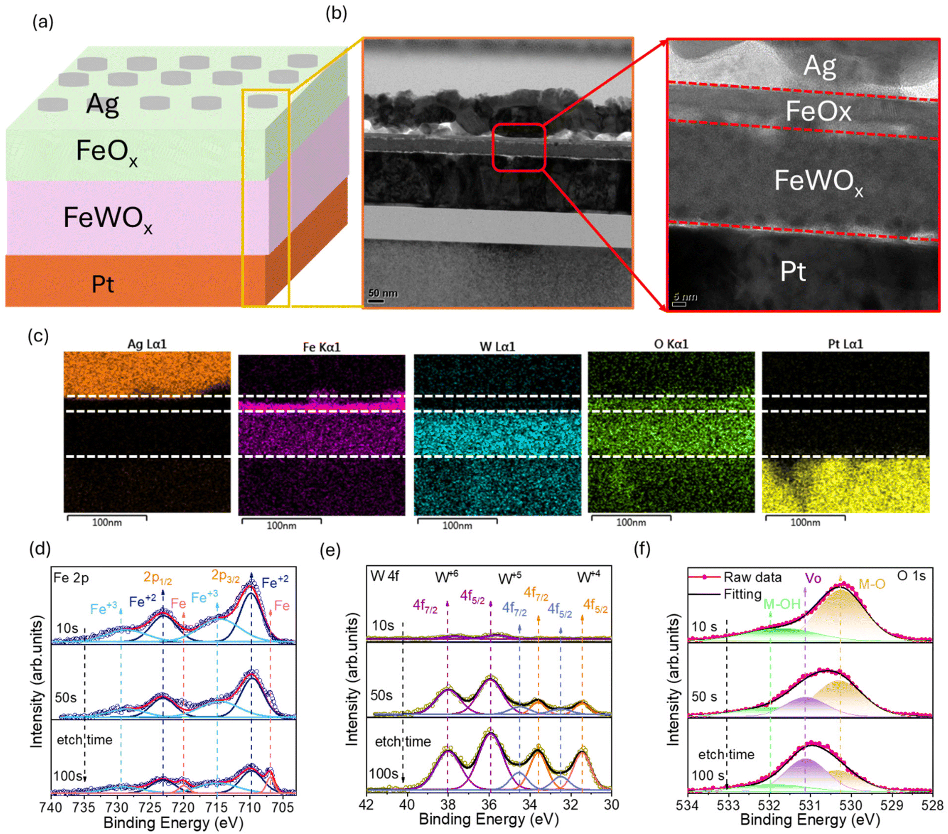 | ||
| Fig. 1 Material characterization of Ag/FeOx/FeWOx/Pt memristor. (a) Schematic representation of the device structure. (b) HRTEM image with an inset showing a zoomed-in view that clearly reveals the bilayer structure of the FeOx/FeWOx films. (c) Energy-dispersive X-ray spectroscopy (EDS) elemental color mapping image confirming the presence and distribution of Ag, Fe, W, O, and Pt in different layers. (d–f) XPS spectra of the FeOx/FeWOx films after etching for 10 s, 50 s, and 100 s, displaying the core-level electron spectra of (d) Fe 2p, (e) W 4f, and (f) O 1s, respectively. | ||
The X-ray photoelectron spectroscopy (XPS) analysis of Fe, W, and O elements at various etching times (10 s, 50 s, and 100 s) is presented in Fig. 1(d–f). The core-level peaks for Fe 2p, W 4f, and O 1s were deconvoluted using Gaussian–Lorentzian (G–L, 5%) fitting to discern the various oxidation states present within the films. The W 4f spectra, as shown in Fig. 1(e), can be deconvoluted into two primary doublets. The main peaks, centered at binding energies of 35.9 eV and 38 eV, correspond to the W 4f7/2 and W 4f5/2 states, respectively, confirming the presence of W6+ in stoichiometric WO3. These binding energies align with reported values for WO3, with the energy separation between the W 4f7/2 and W 4f5/2 peaks measuring 2.1 eV, consistent with established literature.38–41 Additionally, lower-intensity shoulders at reduced binding energies suggest the presence of W5+ and possibly W4+ components, indicative of sub-stoichiometric WOx. The secondary doublet peaks at 34.55 eV and 32.5 eV, associated with the W5+ oxidation state, further support the presence of non-stoichiometric WOx, while a third doublet with peaks at 31.45 eV and 33.6 eV corresponds to the metallic W0+ state.39,40 The intensity of these peaks increases with etching time, being most prominent at 100 s and least at 10 s, with the W5+ and W4+ shoulders becoming more discernible at longer etching durations (50 s to 100 s).
Fig. 1(d) illustrates the XPS spectra for Fe 2p at etching times of 10 s, 50 s, and 100 s. The two main peaks at 710 eV and 724 eV are attributed to Fe 2p3/2 and Fe 2p1/2, respectively. The first doublet, at 709.8 eV and 723.1 eV, indicates the Fe2+ oxidation state, suggesting the presence of non-stoichiometric FeOx.42 The second doublet, observed at 714.6 eV and 728.6 eV, corresponds to the Fe3+ oxidation state, which is characteristic of stoichiometric Fe3O4.43 A third doublet, at approximately 706.9 eV and 720 eV, may be indicative of metallic Fe within the film. Fig. 1(f) shows the O 1s XPS spectra for the FeOx and FeWOx nanocomposite films at different etching times. The O 1s signal was deconvoluted into three components using Gaussian fitting. The first component, with a binding energy of 530.35 eV, is assigned to oxygen atoms in the FeWOx nanocomposite.40 The second component, observed at 531.05 eV, corresponds to oxygen in sub-stoichiometric FeOx, while the third component, at 531.2 eV, is attributed to oxygen in water molecules adsorbed on the film surface. These XPS analyses provide a comprehensive understanding of the complex chemical composition and oxidation states within the FeOx/FeWOx nanocomposite film, offering valuable insights into the material's properties and behavior.
The electrical resistive switching (RS) characteristics of the hybrid nanocomposite memristors were systematically investigated, as illustrated in Fig. 2. Fig. 2(a) depicts the typical volatile threshold switching behaviors, showcasing multiple direct current (DC) current–voltage (I–V) curves recorded at a relatively low current compliance (CC) of 10 μA. The memristor device demonstrates unidirectional switching from a high resistance state (HRS) to a low resistance state (LRS) during the set process, followed by an automatic return to the HRS without the need for an external bias. This behavior is likely due to the spontaneous dissipation of thin and stable nanoscale conductive filaments. The stability of the volatile RS behavior was confirmed over more than 120 continuous switching cycles. The switching voltages were extracted from these cycles and are presented as a histogram in Fig. 2(b), where the average set voltage is approximately 0.09 V, with a standard deviation (σ) of 0.011, derived from Gaussian fitting. Notably, this threshold set voltage is lower than that reported for 2D memristors in previous studies.44,45 As depicted in Fig. S1,† the I–V characteristics and endurance performance of the Ag/FeWOx/Pt memristor were evaluated under varying current compliance levels of 10 μA, 100 μA, and 1 mA. It was observed that the bilayer memristors required higher set voltages to transition from HRS to LRS, with compromised stability in both states. In contrast, the Ag/FeOx/FeWOx/Pt memristor exhibited superior performance, with lower set voltages required for switching between HRS and LRS, indicating more efficient and reliable switching behavior. Furthermore, the Ag/FeOx/FeWOx/Pt memristor demonstrated current compliance-controlled threshold switching, precise control over the switching process, analog switching behavior for continuous regulation of device current, and reliable digital switching characteristics. These attributes make the Ag/FeOx/FeWOx/Pt memristor highly versatile and well-suited for both volatile and nonvolatile memory, as well as neuromorphic computing applications.
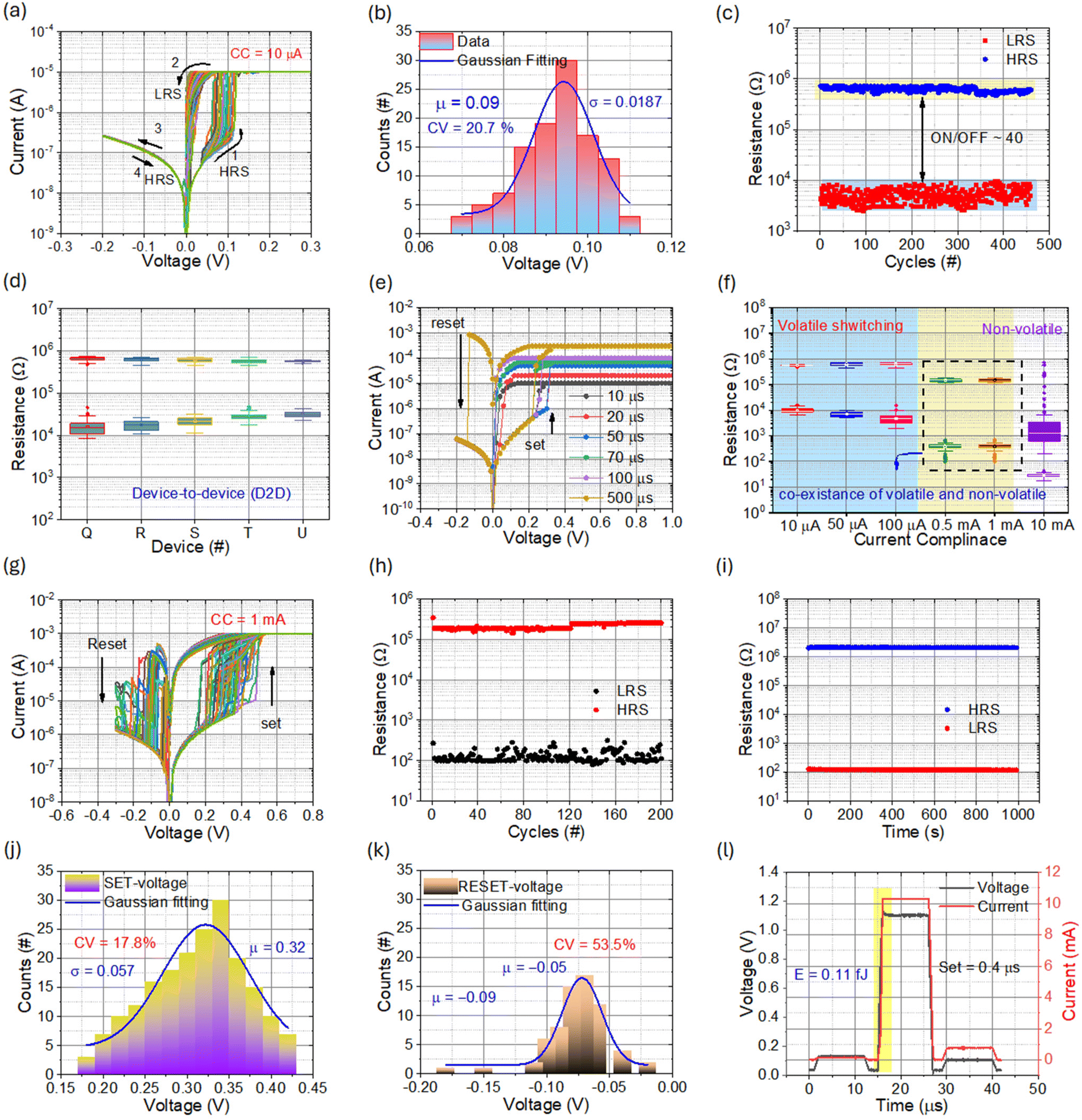 | ||
| Fig. 2 Electrical performance of the memristor. (a) Semi-log I–V curves demonstrating stable volatile switching behavior under low compliance current (CC) over ∼120 consecutive cycles. (b) Histogram of voltage distribution derived from (a), indicating an average set voltage of ∼0.09 V. (c) Endurance plot obtained at 0.02 V, showing consistent distribution of HRS and LRS. (d) D2D variability of nine devices, showing endurance test results in volatile switching mode at a CC of 10 μA. (e) I–V curves under positive and negative voltage regions at various CC values. (f) Relationship between device resistance and CC, illustrating the transition from volatile to coexistence of volatile and non-volatile switching, and finally to non-volatile switching, as observed during cycling tests. (g) Typical non-volatile I–V curves under a CC of 1 mA. (h) Corresponding distributions of HRS and LRS over 200 switching cycles. (i) Retention characteristics. (j and k) Cumulative probability plots of set and reset voltages determined from 200 consecutive switching cycles, showing variation in non-volatile RS behavior. (l) Switching response time and power consumption during the set process, evaluated under pulse test mode. | ||
Fig. 2(c) presents the endurance data over 500 DC cycles, demonstrating the performance stability of our device. The HRS and LRS, extracted at a read voltage of 0.02 V, show an ON/OFF ratio of 102, indicating reliable switching characteristics. Notably, the LRS exhibits minimal fluctuation throughout the endurance test, while the HRS remains stable. Additionally, Fig. 2(d) and Fig. S2† depict the results of a 100-cycle endurance test for nine memristor devices, revealing consistent characteristics across all devices and indicating excellent device-to-device (D2D) reliability. Fig. 2(e) presents the I–V curves under positive and negative bias, with varying current compliance from 10 μA to 500 μA, illustrating volatile switching behavior at low CC and nonvolatile behavior at high CC. From these I–V curves, it is evident that the transition from volatile to nonvolatile RS occurs at a CC of 500 μA, confirming volatile RS at CCs of 100 μA and below, and nonvolatile RS at CCs of 500 μA and above. This observation suggests that the RS behavior can be modulated from volatile to nonvolatile by adjusting the CC value. In Fig. S2,† we explore the device-to-device (D2D) variability and reproducibility in FeOx/FWOx-based memristors. The Fig. S2† demonstrates typical digital RS behavior observed across different memory devices labelled D1 through D9. The I–V curves, recorded over 100 cycles during the cyclic test, illustrate the sweep direction indicated by arrows and numbers. This analysis provides valuable insights into the consistency and reliability of RS behavior among multiple memristor devices. The corresponding HRS and LRS states are displayed in Fig. 2(f). Throughout the I–V repetitive tests at different CCs, three types of I–V characteristics were identified: complete volatile switching below 100 μA CC, the coexistence of volatile and non-volatile switching behavior at 500 μA and 1 mA CC, and complete non-volatile switching behavior at high CC (10 mA).
Interestingly, Fig. 2(f) shows the resistance of the memristor device as a function of CC, revealing that increasing CC can lead to a transition from volatile switching to the coexistence of volatile and non-volatile switching, and eventually to non-volatile switching. It is noteworthy that the LRS resistance increases as CC is increased, while the HRS remains constant at 1 mA CC but experiences a sudden drop at 10 mA, likely due to the formation of too-thick conductive filaments, resulting in an abrupt decrease in HRS. This behavior, associated with the higher conductivity of residual Ag conductive filaments in the FeOx/FeWOx nanocomposite film, is consistent with observations reported in previous literature.46,47 Once the CC exceeds 500 μA, the memristor device can maintain either the HRS or LRS, requiring a reverse voltage to switch the device back to HRS.
To further evaluate the memory performance of the memristor nonvolatile switching behavior, thorough analyses of its electrical RS characteristics were conducted, as shown in Fig. 2(g–l). Fig. 2(g) presents 100 repeated I–V dual sweep curves of the memristor device under a CC of 1 mA. These curves demonstrate the device ability to switch from HRS to LRS at positive voltage and reset at negative voltage, characteristic of typical bipolar RS behavior. The gradual decrease in current during the reset process can be attributed to Joule heating-assisted electric field effects, which govern the slow oxidation of Ag filaments, resulting in their gradual thinning.48 In Fig. S3,† we explore the D2D variability and reproducibility of the Ag/FeOx/FeWOx/Pt memristor device, showcasing consistent RS behavior across six randomly selected devices. The I–V curves, recorded over 100 cycles at a current compliance of 1 mA, illustrate the sweep direction, providing insights into the consistency and reliability of the memristor devices in exhibiting digital RS characteristics.
Fig. 2(h) presents the results of 200 consecutive cyclic measurements conducted at room temperature, illustrating cell-to-cell (C2C) variation. Both the high resistance state (HRS) and low resistance state (LRS) exhibit narrow distribution ranges, indicating stable and well-controlled formation and rupture of Ag conductive filaments. This stability is attributed to the FeOx/FeWOx bilayer, which supports low-voltage switching in Ag filament-based CBRAM due to several advantageous properties. The FeOx layer, rich in oxygen vacancies, enhances Ag+ ion migration, enabling filament formation at minimal voltage. Meanwhile, the high dielectric constant of FeWOx amplifies the localized electric field, further reducing the voltage required for switching. Additionally, the stable chemical structure of FeOx/FeWOx minimizes defect generation and heat dissipation, contributing to reliable switching at lower voltages. Together, these material characteristics make the FeOx/FeWOx bilayer an ideal medium for efficient, low-power operation in CBRAM devices.
Data retention, a critical parameter for memory applications, was tested over 1000 s with a switching ratio (HRS/LRS or memory window) > 104 using a non-disruptive reading voltage of 0.1 V under open-air conditions, as shown in Fig. 2(i). The steady trend observed suggests that longer lifetimes can be expected from the retention results of HRS and LRS. Additionally, the cumulative distributions of set and reset voltages were analysed, with coefficients of variation of 7.03% and 22.52%, respectively, as shown in Fig. 2(j) and (k). Specifically, the set voltage ranges from 0.2 to 0.56 V, while the reset voltage ranges from −0.02 to −0.18 V, indicating relatively low variability in operation voltages. Finally, device-to-device variability in non-volatile switching mode was investigated, with 100 I–V characteristics plotted in Fig. S3,† demonstrating consistent HRS and LRS values among six devices under identical testing conditions. Fig. 2(l) depicts the response speed characteristics and power consumption during the set process, conducted in pulse test mode. The pulse amplitude and width for setting are 1.2 V and 10 μs, respectively. Notably, the set response time and power consumption were observed to be 20 μs and 0.11 fJ, indicating the promising potential of FeOx/FeWOx nanocomposite-based memristors for practical applications in neuromorphic computing.
Ensuring stability and repeatability over time is crucial for the functionality of memristor devices.49 In this study, we extensively investigated the stability and repeatability of memristor devices over an extended period. The I–V characteristics of the memristor device were examined in ambient atmospheric conditions at three distinct time points: immediately after fabrication (fresh), after six months, and approximately one year later. The objective was to confirm the consistency of the switching behavior and to assess its stability and reproducibility over time. Fig. 3(a–c) present typical I–V curves recorded over 100 cycles for each time point. Remarkably, no significant degradation in the RS characteristics was observed, even after continuous cycling over 100 repetitions, indicating robust performance over time. Further endurance testing, as depicted in Fig. 3(d) and (f), confirmed that both the HRS and LRS remained unchanged and stable across different time intervals. The histograms of the HRS and LRS resistance values distribution, shown in Fig. 3(g–i), reveal consistent resistance values over time. Gaussian fits of the histograms indicate low coefficients of variation for both HRS (approximately 12.8%) and LRS (approximately 3.8%) after six months of testing, signifying minimal fluctuations in resistance values from cycle to cycle (C2C). Additionally, a detailed analysis of the threshold voltages over 100 cycles was conducted, with the resulting distribution histograms illustrated in Fig. 3(j–l). These histograms demonstrate that the SET voltage became more centralized after six months of testing, facilitating precise control of the SET programming voltages for device applications. Our findings underscore that memristor devices exhibit remarkable stability and repeatability over time, even one-year post-fabrication. This exceptional performance highlights their potential for practical applications, particularly in nonvolatile memory and neuromorphic computing.50 The ability to adjust the LRS resistance by varying the CC further enhances their utility for error-free multilevel data storage applications.51–53 Through our comprehensive investigation, we provide valuable insights into the long-term performance and reliability of memristor devices, paving the way for their widespread adoption in various technological domains.
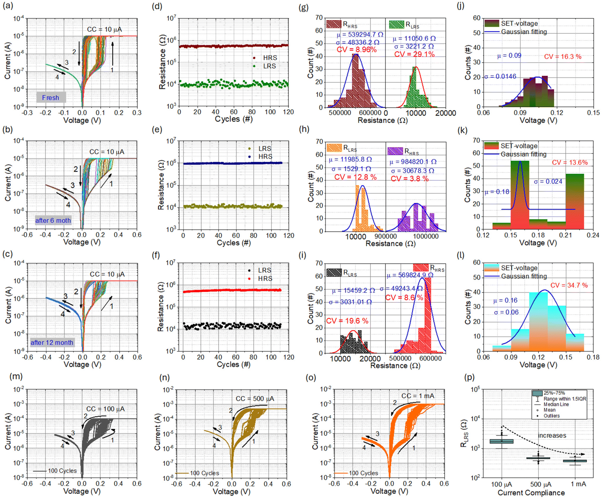 | ||
| Fig. 3 Stability and reproducibility tests of the memristor device across different time intervals. I–V switching cycles are shown for 120 consecutive cycles under varying conditions: (a) fresh, (b) after six months, and (c) approximately one year later. Endurance performance over 120 cycles is depicted for each time point: (d) fresh, (e) after six months, and (f) approximately one year later. Histograms displaying the distribution of HRS and LRS resistance values are presented for (g) fresh, (h) after six months, and (i) approximately one year of operation. The cumulative probability distribution of the set voltage is illustrated for (j) fresh, (k) after six months, and (l) approximately one year, with Gaussian fits shown by the blue lines. Comparative analysis of 100 I–V cycles is conducted on memristors subjected to different compliance currents (CCs) of (m) 100 μA, (n) 500 μA, and (o) 1 mA. The statistical evaluation of the LRS in relation to various CCs is presented in (p). | ||
Furthermore, our study elucidates the significance of CC in regulating the resistance states of memristor devices. Fig. 3(m–o) illustrate 100 consecutive I–V curves obtained from memristors subjected to different CCs during the SET process, resulting in distinct LRS levels. We observed that increasing CC values led to the formation of thicker conductive filaments, which consequently resulted in lower resistance values in both the LRS and HRS states.54–56 Notably, the HRS state values remained relatively constant across all tested CC values, indicating consistent performance under varying compliance conditions. The clear differentiation among four distinct resistance states, including one HRS and three LRS states, underscores the ability of memristor devices to retain volatile switching behavior while accommodating multilevel data storage requirements. These findings confirm the presence of modified multilevel conductance in memristive devices, thereby enhancing their potential for high-density data storage applications. Our comprehensive analysis highlights the robust stability, repeatability, and versatility of memristor devices, making them highly suitable for a wide range of technological applications.57,58 The insights gained from our study contribute significantly to advancing the understanding of memristor device behavior over extended periods, paving the way for their integration into various emerging technologies.
In the memristor system, the top and bottom electrodes emulate presynaptic and postsynaptic neurons, analogous to biological synapses where synaptic weight adjusts with neurotransmitter strength.10 Synaptic plasticity in biological systems involves the potentiation or depression of synaptic weight for information processing.59 This behavior is emulated in memristor devices, where pulsing modulates the conductive channel to precisely regulate conductance, representing changes in synaptic weight. In this study, we demonstrate the manipulation of volatile, digital, and analog switching characteristics by controlling the CCs during the set process. Various switching behaviors were achieved by modulating conductance, making these devices suitable for neuromorphic applications.60 Initially, 100 DC switching cycles were executed in volatile switching mode, as shown in Fig. 4(a) Volatile switching behavior allowed gradual conductance adjustment by applying 50 positive pulses with an amplitude of 0.85 V under varying pulse widths. Fig. 4(b) illustrates the gradual increase in conductance with increasing pulse width. Additionally, the response current increased with the number of pulses when 50 pulses with different amplitudes (+0.85 to +1.15 V) were applied to the memristor device, as shown in Fig. 4(c). This observation aligns with previous studies by Wang et al., which indicate that the strength of Ag-based conductive filaments is highly controllable and can be effectively modulated by pulse amplitude. This modulation is crucial for mimicking short-term memory behavior in neuromorphic computing. A pulse endurance test, conducted over 1000 cycles, demonstrated no significant degradation, as illustrated in Fig. 4(d). A 1 μs pulse width for both set and reset pulses, with amplitudes of 0.9 V and −0.8 V, was applied to the memristor devices, which exhibited stable conductance values in both LRS and HRS during switching operations.
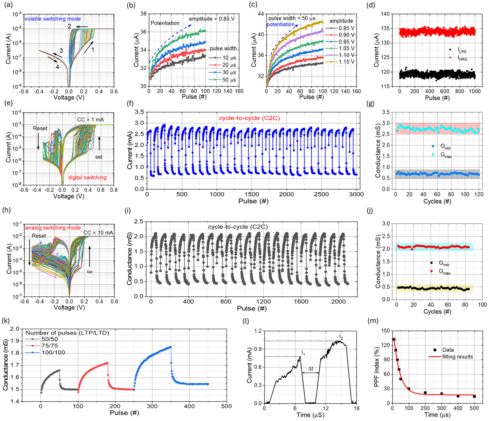 | ||
| Fig. 4 Neuromorphic behavior of the Ag/FeOx/FeWOx/Pt memristor, focusing on modulation switching behavior in DC mode and under pulse stimulation. (a) Consecutive 100 DC sweeps showing I–V characteristics in volatile switching mode. The current response indicates potentiation under voltage pulses for varying (b) Pulse widths and (c) Pulse amplitudes. (d) Synaptic endurance assessment following volatile switching mode. (e) I–V curves of 100 repetitive switching cycles demonstrating digital behavior. (f) Potentiation and depression conductance states modulated by 50 consecutive identical positive pulses (amplitude: +0.85 V, width and interval: 1 μs) and 50 consecutive identical negative pulses (amplitude: −0.85 V, width and interval: 1 μs) in digital mode operation. (g) Variation of Gmax and Gmin during the potentiation and depression processes over 110 cycles. (h) I–V curves of 100 repetitive switching cycles demonstrating analog mode behavior. (i) Conductance modulation under repeated potentiation and depression pulses to mimic synaptic weight transitions in analog mode operation. (j) Variation of Gmax and Gmin during the potentiation and depression processes over 90 cycles. (k) Potentiation and depression processes under various pulse sets (50, 75, and 100 pulses). (l) EPSC triggered by a pair of 1.0 V/10 μs pulses. (m) PPF index as a function of the time interval (Δt) between voltage spikes of 1.0 V. | ||
Before initiating pulse operations to characterize potentiation and depression, the memristor underwent a thorough establishment of digital switching behavior through continuous execution of 100 cycles. During this process, a CC of 1 mA was maintained, with fixed positive set and negative reset voltages (set = 0.3 V, reset = −0.3 V), as shown in Fig. 4(e). The memristor exhibited abrupt switching behavior during these 100 sets and reset operations, indicating successful establishment of digital switching behavior. To emulate biological synaptic function, a pulse test using identical 50 potentiation and depression pulse trains was conducted, as shown in Fig. 4(f) The potentiation and depression pulse amplitudes and widths were set to ±0.3 V and 1 μs, respectively. The memristor successfully achieved potentiation and depression with abrupt increases and decreases in conductance. The stability and reproducibility of these processes were confirmed over 100 continuous pulse cycles, as shown in Fig. 4(g), with mean Gmax potentiation and Gmin depression values of 2.67 mS and 0.71 mS, respectively.
It is widely acknowledged that gradual transitions during the set and reset processes lead to gradual changes in conductance, which are essential for potentiation and depression phenomena.61,62 Accordingly, we increased the CC to 10 mA, as previous studies have indicated that higher CCs promote the formation of thicker conductive filaments, facilitating gradual switching.62Fig. 4(h) illustrates 100 continuous switching cycles under a CC of 10 mA, revealing a gradual switching behavior during the set and reset processes after several cycles. This observation suggests the establishment of thicker conductive filaments through repeated switching cycles, making the I–V curves suitable for pulse operations in neuromorphic applications. However, it is noteworthy that under these conditions, the on/off ratio of the memristor devices tends to decrease, which is advantageous for achieving gradual conductance changes.62 As shown in Fig. S4(a),† the reset operation was performed in DC scanning mode with a cutoff voltage ranging from −0.2 V to −0.3 V in −0.01 V increments. A continuous decrease in device current was observed, demonstrating the analog switching characteristics of the memristor. Fig. 4(i) presents typical potentiation and depression curves obtained by gradually altering conductance using identical pulses. Specifically, 50 set and reset pulses with amplitudes of 0.4 V and −0.3 V, and widths of 1 μs and 2 μs, respectively, were applied. The potentiation and depression effects were demonstrated over more than 20 consecutive cycles, resulting in gradual conductance changes. The reproducibility of synaptic behaviors is crucial for implementing synaptic devices; thus, an endurance test was conducted with approximately 90 repetitive potentiation and depression cycles, achieved through 50 sets of continuous set and reset pulses, as depicted in Fig. 4(j). Repetitive potentiation and depression behaviors were achieved with negligible variations in conductance values between Gmax and Gmin states. The average Gmax and Gmin values were 2.08 mS and 0.456 mS, respectively. Similar results were observed by Yang et al.63 who calculated Gmax and Gmin states during cycling tests for the potentiation and depression processes.
Additionally, variability in conductance states among memristor devices during both potentiation and depression processes was observed across 12 randomly selected devices, as shown in Fig. S4(b).† This variability highlights the inherent differences between individual devices under identical conditions. Fig. S4(c)† further examines the variation in Gmax and Gmin values during the potentiation and depression processes across 50 devices, providing a comprehensive understanding of performance consistency and potential deviations in a larger sample set. These results underscore the importance of modulating pulse width, amplitude, and number to enhance memory levels by controlling the movement of Ag ions at the interface of the FeOx/FeWOx nanocomposite-based memristor.
Paired pulse facilitation (PPF), a common form of synaptic plasticity in neurobiology, manifests as short-term plasticity (STP), which is crucial for decoding temporal information in the brain.64Fig. 4(k) illustrates the response current versus time, showing input pulses with an amplitude and width of 0.95 V and 10 μs, respectively, applied to the memristor devices. The response current induced by the second input pulse surpassed that of the first, resembling the PPF phenomenon observed in biological synapses.59 This observation suggests that the rapid succession of two pulses leads to continuous accumulation of Ag ions after the initial filament formation during the first pulse, which may eventually strengthen existing filaments and promote the formation of new ones, thereby enhancing conductivity. Fig. 4(l) depicts the calculated PPF index as a function of the interval between paired pulses, with pulses fixed at 0.95 V and 10 μs The PPF index is defined as PPF index = (I2/I1) × 100%, where I2 and I1 represent the response conductivity induced by the second and first input pulses, respectively.65 Specifically, the PPF index decreased from 132.2% to 14.3% as the pulse interval increased from 10 μs to 500 μs, fitting well to an exponential regression represented by the black line in Fig. 4(m). Thus, increasing the pulse interval exponentially decreases the degree of response facilitation provided by the memristor device.59
Fig. 5 reveals the synaptic plasticity exhibited by the memristor device, mimicking the behavior of biological synapses, where the excitatory postsynaptic current (EPSC) is modulated not only by pulse amplitude and width but also by pulse interval.65 To further explore the modulation properties of EPSC, a series of positive pulse sequences with varying amplitudes, widths, and intervals were applied. Fig. 5(a–c) present the EPSC responses to consecutive excitatory pulses, showcasing modulation with varying pulse amplitudes, widths, and intervals, respectively.
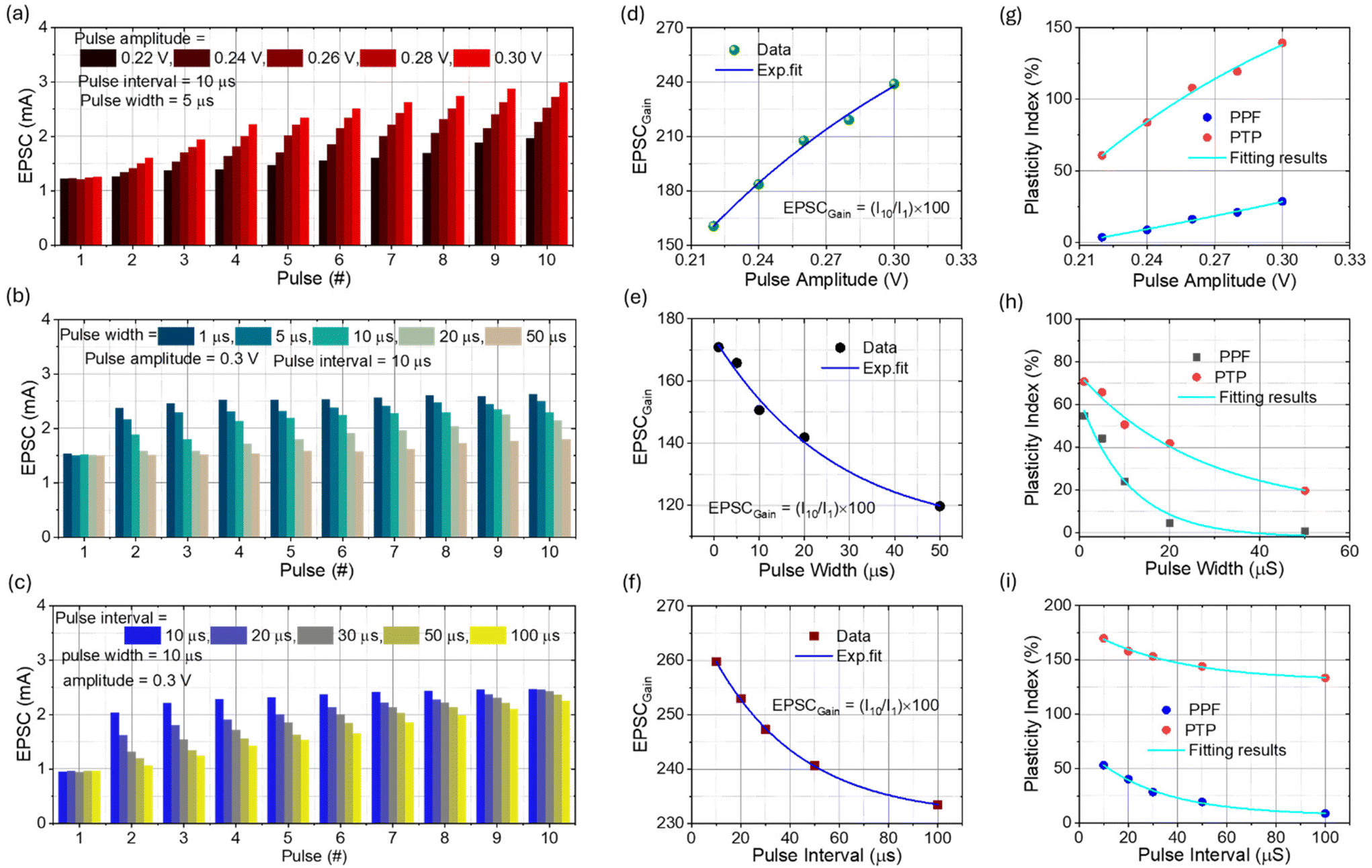 | ||
| Fig. 5 Experimental validation of fundamental biological synaptic functions for neuromorphic computing, providing an in-depth analysis of SRDP in the memristor device. EPSC responses were examined under various identical pulses, including: (a) a range of amplitudes from 0.22 to 0.3 V (with a constant pulse width of 5 μs and interval of 10 μs), (b) widths ranging from 1 to 50 μs (while maintaining a constant pulse amplitude of 0.3 V and interval of 10 μs), and (c) intervals spanning from 10 to 100 μs (with a constant pulse amplitude of 0.3 V and width of 10 μs). The relationship between EPSC gain and (d) pulse amplitudes, (e) pulse widths, and (f) pulse intervals provide valuable insights into synaptic plasticity dynamics. Additionally, the correlation between the synaptic plasticity index and (g) pulse amplitudes, (h) pulse widths, and (i) pulse intervals offer further understanding of the underlying mechanisms. Moreover, the mean ΔI after consecutive pulses (ΔI = (I2 − I1)/I1) and after the tenth pulse (ΔI = (I10 − I1)/I1) versus the amplitude, width, and interval of the applied bias pulse reveal key aspects of PPF and PTP, respectively. | ||
During the pulse amplitude spike-rate dependent plasticity (SRDP) measurement, positive set amplitudes ranging from 0.22 V to 0.33 V were applied with a constant pulse width and interval of 5 μs and 10 μs, respectively. Notably, the EPSC increased with higher pulse amplitudes, indicating a rapid rise in EPSC at higher amplitudes and a contrasting trend at lower amplitudes, consistent with SRDP characteristics.66Fig. 5(b) and (c) elucidate the relationship between EPSC and pulse width, as well as pulse interval, respectively. The EPSC exhibits a decreasing trend with increasing pulse width (pulse amplitude of 0.3 V and pulse interval of 10 μs) and interval (pulse amplitude of 0.3 V and pulse width of 50 μs). Higher EPSC levels are observed at lower pulse width and interval values, indicating a higher frequency of current changes. These observations align with SRDP principles, suggesting a successful emulation of synaptic plasticity mechanisms.
Furthermore, the EPSC gain, defined as the ratio of the tenth pulse current to the first pulse current (I10/I1), increases with increasing pulse amplitude, width, and interval, as shown in Fig. 5(d–f). These findings underscore the intricate relationship between pulse parameters and synaptic plasticity, resembling high pass filtering akin to biological synapses. Fig. 5(g–i) provide further insights into this relationship by introducing parameters such as PPF and post-tetanic potentiation (PTP),67 which are defined by the equations PPF = ((I2 − I1)/I1) × 100% and PTP = ((I10 − I1)/I1) × 100%, respectively. The observed changes in output current response are analogous to the PPF and PTP phenomena of a biological synapse, influenced by pulse amplitude, width, and interval. The relaxation process of conducting filaments within the switching layer, driven by Ag ion accumulation, is proposed as a potential explanation for the pulse interval-dependent behavior observed in the artificial synapse. In this scenario, the collapse or persistence of conducting filaments governs the changes in device output current.68
In biological neural systems, synaptic plasticity plays a pivotal role in memory formation and retention, reflecting the dynamic connections between neurons in the brain.69Fig. 6(a) provides a simplified depiction of a biological synapse, while Fig. 6(b) presents a model illustrating the intricate processes of learning and memory. According to this model, incoming information is initially encoded as short-term memory (STM) and can be transferred into long-term memory (LTM) through maintenance rehearsal.70,71 To emulate these fundamental processes, our study investigated the influence of pulse parameters on memory transitions using memristor devices. Fig. 6(c) clearly illustrates the transition from STM to LTM under varying pulse amplitudes (0.65 V to 0.9 V). As the amplitudes increase, the synaptic weight rises from 7.9 μA to 15.8 μA, likely due to oxidation at the electrode interface. This observation is further supported by Fig. 6(d), where EPSC gain is shown to increase with pulse amplitudes. Specifically, EPSC gain increases from 122.4% to 168.3% as pulse amplitudes rise from 0.65 V to 0.9 V, highlighting the memristor device's ability to encode information across multiple states, contributing to the nuanced dynamics between STM and LTM.11 Moving forward, Fig. 6(e) illustrates the evolution from STM to LTM under different pulse widths (10 μs to 500 μs), with consistent pulse amplitude (0.85 V) and interval settings (100 μs). Notably, wider pulse widths correspond to heightened EPSC values, indicating a clear trend towards LTM. This finding underscores the adaptability of memristor devices in mimicking LTM behavior through pulse width adjustments. Additionally, Fig. 6(f) depicts the augmentation of EPSC gain with increasing pulse width, affirming the enhanced synaptic plasticity of the memristor device and its ability to transition from STM to LTM.3
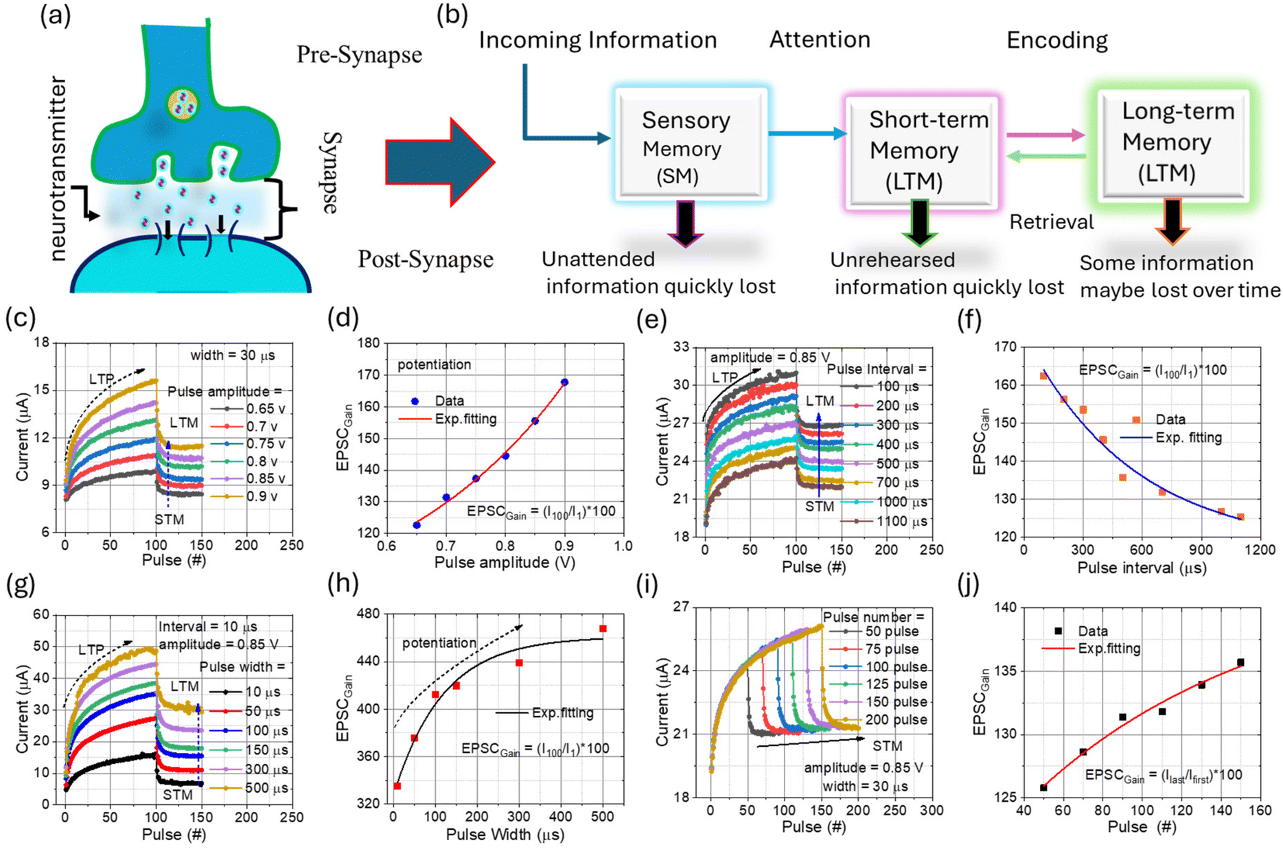 | ||
| Fig. 6 Exploration of the enhancement from STM to LTM through repeated stimulation, offering a detailed view of synaptic behavior. (a) A simplified schematic of a biological synapse sets the context for understanding the neural processes under study. (b) A typical learning and memory model illustrates the nuanced behaviors of STM and LTM in brain function. (c) The transition from STM to LTM is examined under varying pulse amplitudes (0.65 to 0.9 V), with fixed pulse width and delay time, highlighting the dynamic nature of memory consolidation. (d) Corresponding EPSC gain (I100/I1) reveals the impact of pulse amplitudes on memory transition, emphasizing amplitude-dependent synaptic plasticity. (e) Further investigation into the STM to LTM transition under varying pulse widths (ranging from 10 μs to 500 μs) with fixed pulse amplitude and interval, providing insights into the temporal dynamics of memory formation. (f) EPSC gain variation with pulse width demonstrates the relationship between temporal parameters and memory consolidation. (g) Examination of STM to LTM transition under varying pulse intervals (ranging from 100 μs to 1100 μs) with fixed pulse width and amplitude, offering additional perspective on the temporal modulation of synaptic memory. (h) EPSC gain variation with pulse interval underscores the temporal dynamics inherent in memory enhancement. (i) Exploration of STM to LTM transition under different pulse numbers (ranging from 50/50 to 200/200) with fixed pulse width, interval, and amplitude, shedding light on the cumulative effect of repeated stimulation on memory consolidation. (j) Variation of EPSC gain with pulse number highlights the exponential nature of memory enhancement with increased stimulation. | ||
Further exploration of temporal dynamics involved varying pulse intervals (100 μs to 1100 μs), as shown in Fig. 6(g). The observed increase in EPSC relaxation with longer intervals suggests a gradual generation of Ag+ ions during relaxation, while the corresponding decrease in EPSC gain reflects STM-like characteristics. Fig. 6(h) extends this investigation by examining the impact of pulse intervals on the STM to LTM transition. Longer intervals lead to a gradual decrease in synaptic weight, reminiscent of STM properties, accompanied by a reduction in EPSC gain, indicating a diminishing transition towards LTM. Additionally, we explored the impact of increasing the number of pulses on memory transitions, as illustrated in Fig. 6(i). With each successive increase in the number of pulses, there was a corresponding elevation in EPSC values, attributed to the effective accumulation of Ag ions at the interface. However, despite this incremental rise in EPSC, the transition from STM to LTM was not evident with the increased number of pulses. Interestingly, Fig. 6(i) shows an upward trend in EPSC with the addition of more pulses, while the relaxation time remained consistent. This observation suggests that while pulse number influences STM behavior, it does not notably impact the transition to LTM. The corresponding EPSC gain, calculated as the ratio of I100 (postsynaptic current after 100 pulses) to I1 (postsynaptic current after the first pulse), is presented in Fig. 6(j). Notably, during the potentiation process, EPSC gain shows an increasing trend within the first 100 pulses. However, as demonstrated in Fig. 6(j), EPSC values during potentiation remain relatively constant during relaxation, indicating a lack of transition from STM to LTM. Our findings highlight the remarkable potential of memristor devices in emulating synaptic plasticity and memory transitions akin to biological synapses, paving the way for advancements in neuromorphic computing and artificial intelligence.72,73
The implementation of reservoir computing (RC) on our memristor devices was pursued, leveraging the STM effect arising from volatile switching behavior.74,75 RC is a computational paradigm designed for processing temporal and sequential data, enabling tasks such as time-series forecasting and pattern generation. Fig. 7(a) presents a schematic of the RC system, comprising input, reservoir, and output layers. The input layer encodes incoming time-dependent data into the resistance values of memristor cells within the reservoir, while the reservoir layer serves as a dynamic computational medium, transforming input signals into high-dimensional output through nonlinear transformation. The output layer generates the desired output or prediction based on the information processed in the reservoir layer.
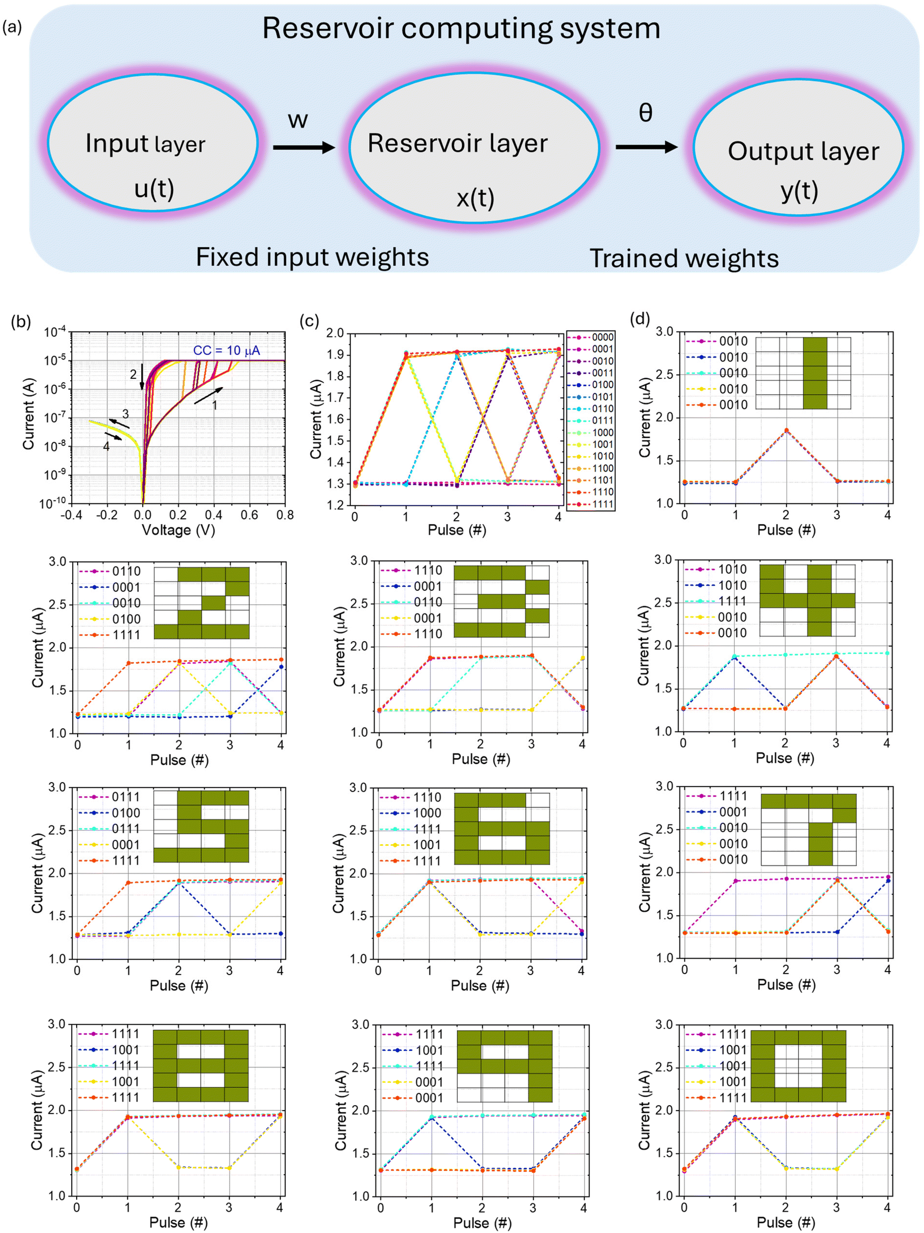 | ||
| Fig. 7 Integration of reservoir computing (RC) systems into our memristor devices. (a) Schematic of the RC system, highlighting a reservoir with internal dynamics and a readout function. Only the weight matrix connecting the reservoir state u(t) and the output y(t) requires training. Additionally a schematic of the RC system with pulse streams as inputs, the memristor reservoir, and a readout network. For a simple digit recognition task using 5 × 4 images, the reservoir comprises 9 memristors. (b) 50 consecutive thresholds switching observed prior to RC system implementation. (c) Sixteen distinct states acquired through RC implementation. (d) Experimentally measured reservoir states representing digits 0 to 9, along with experimental potentiation and relaxation classifications. Insets feature images of the 10 digits used in this test. | ||
To encode 4-bit data, time-dependent pulse train inputs were applied to five devices, as depicted on the left side of Fig. 7(a). The transient modification of synaptic weight in the memristor device under STM characteristics enables it to represent 4-bit data by detecting changes in current states through read pulses following the inputs. For the RC system, threshold switching behaviors were achieved at a lower CC of 10 μA, as demonstrated in Fig. 7(b). Volatile weak conductive filaments formed at the FeOx/FeWOx switching matrix under low CC, leading to reversible resistance changes during voltage sweeps. Reliable 50-cycle volatile switching was repeated before initiating the RC test, mimicking the transient modifications observed in STM.
Fig. 7(c) illustrates the sixteen distinct states ranging from [0000] to [1111], obtained by applying set pulses to the memristor device, with appropriate read pulses following. Sequential pulse application generated these 16 different states of RC, ensuring minimal impact of prior inputs on subsequent outputs. Additionally, as shown in Fig. S5,† we tested 16 states of reservoir input signals on four randomly selected memristor devices to demonstrate the reproducibility of the RC system. This analysis confirms the consistent performance of the memristor devices across different input states, highlighting their reliability for reservoir computing applications.
Fig. 7(d) shows the representation of digits 0 to 9 in the form of 5 × 4 pixels, with current outputs displayed after applying pulse sequences. Each digit representation was systematically achieved by corresponding temporal inputs, with the memristor device acting as a physical reservoir due to its volatile nature. The distinct conductance states in response to different pulse sequences confirm the memristor's capability within the RC system. The final output currents for each digit validate the reservoir's capacity to distinctly represent all ten digits based on unique conductance states. To confirm the reproducibility of the RC system, we tested another memristor device using digits 1 to 9, represented as 5 × 4-pixel reservoir states, as shown in Fig. S6.† The current response to each individual pulse from five basic pulse sequences demonstrates the device's ability to differentiate between multiple inputs. The insets display the images labelled 1 through 9 used in this test, highlighting the memristor's response to each specific input.
Fig. 8 illustrates the implementation of RC using an Ag/FeOx/FeWOx/Pt memristor device as a physical reservoir. RC is renowned for its parallel information processing capabilities, excelling in fields such as image recognition, speech recognition, and image processing. Fig. 8(a) depicts the handwritten digit “3” from the Modified National Institute of Standards and Technology (MNIST) database, including the original image and its processing stages. Fig. 8(b) shows a schematic diagram of the deep neural network (DNN) used in our model, configured as a multi-layer perceptron with 196 input neurons, 100 hidden neurons, and 10 output neurons. In this model, RC consists of three layers: the input layer, the reservoir layer, and the readout layer, each performing distinct functions. The input layer processes images for high-dimensional mapping to the reservoir layer.76,77
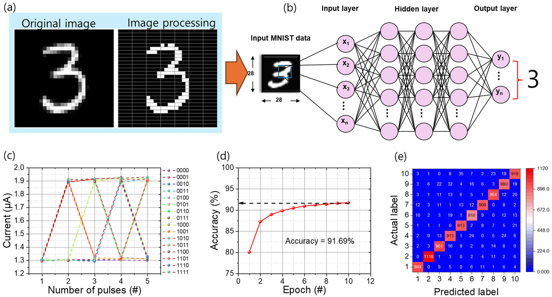 | ||
| Fig. 8 (a) Illustration of the handwritten digit “3” from the MNIST database, including the original image and its processing stages. (b) Schematic diagram of the deep neural network (DNN) used to implement the proposed reservoir computing (RC) system for digit classification, featuring a multilayer perceptron with three hidden layers between the input and output layers. (c) Current value response for 4-bit reservoir computing data. (d) Accuracy data obtained after 10 training epochs with the 4-bit reservoir computing model. (e) Confusion matrix based on 10000 new test images at the end of training using the Ag/FeOx/FeWOx/Pt memristor device. | ||
In our simulation, using the Modified MNIST database, pixel values of each image were binarized and grouped according to a 4-bit model. This process involved transforming the 28 × 28-pixel images into 7 × 28-pixel groups, with each group assigned one of 16 possible states from [0000] to [1111]. These processed images were then mapped into 196 virtual arrays in the reservoir layer, where high-dimensional mapping occurs. The data was normalized using 4-bit conductance values, as shown in Fig. 8(c). The output values from the reservoir layer were trained in the readout layer, a simple multi-layer perceptron DNN consisting of 196 input neurons, 100 hidden neurons, and 10 output neurons. Fig. 8(d) presents the accuracy profiling results over 10 training epochs with 60000 training images. As training progresses, accuracy stabilizes, ultimately achieving 91.69%. Fig. 8(e) shows the confusion matrix for the model when tested with 10000 new images, demonstrating an average accuracy of 93.28% across all labels.
Additionally, we employed a Convolutional Neural Network (CNN) to identify the digit ‘3’, utilizing potentiation and depression conductance data to simulate accuracy accumulation. As shown in Fig. S7,† the CNN achieved an accuracy of 93.4% after 20 epochs with 60000 training images, closely aligning with the accuracy obtained using the DNN in our reservoir computing system. By comparing the performance of both CNN and DNN models, we found a consistent correlation in training results, underscoring the effectiveness of our Ag/FeOx/FeWOx/Pt memristor-based reservoir computing system for efficient image recognition. Table S1† provides a comparative analysis with other CBRAM-based bilayer structures, detailing essential parameters like switching speed, operating voltage, and compliance current dependency. This comparison underscores FeOx/FeWOx specific benefits for low-power and tuneable switching performance. For further insights, please refer to the ESI,† where a detailed explanation and additional comparative data are provided.
Conclusions
In conclusion, our study highlights the Ag/FeOx/FeWOx/Pt memristor as a versatile and promising device for a wide range of computing applications. We successfully demonstrated its electroforming-free volatility and nonvolatility switching capabilities through compliance current modulation and structural engineering, establishing its suitability for neuromorphic, in-memory, and reservoir computing tasks. The memristor's low operating voltage, uniform switching behavior, excellent retention, and multilevel switching capability position it as a compelling candidate for high-density memory applications. Furthermore, our study illustrates the memristor's ability to emulate key synaptic functions, including long-term potentiation and depression, paired-pulse facilitation, and spike amplitude/width/interval dependent plasticity. These features enable its integration into neuromorphic computing systems, where it can effectively mimic the dynamic behavior of biological synapses to support learning and adaptation processes. In addition, we demonstrated the memristor's performance in image recognition tasks, specifically through its implementation in a 5 × 4-digit image recognition system, showcasing its potential for real-world applications. Our study also revealed the controlled transition from short-term to long-term memory within the memristor, offering flexibility in memory storage. The memristor's volatile switching behavior further proves its utility in reservoir computing, acting as a dynamic reservoir with interconnected nodes for sequence data classification tasks. To validate the efficiency of our implemented reservoir computing system, we conducted off-chip training using a DNN with a physical reservoir, achieving a recognition rate of 93.4%. The coexistence of volatile and non-volatile switching in the Ag/FeOx/FeWOx/Pt memristor expands the horizons of memristive device technology, opening new opportunities for the development of advanced computing systems. This study underscores the potential of memristor-based technologies in driving innovation across various computational domains, particularly in areas requiring efficient, scalable, and adaptive computing solutions.Data availability
The authors confirm that the data supporting the findings of this study are available within the article and its ESI.† Raw data that support the findings of this study are available from the corresponding author, upon reasonable request.Conflicts of interest
There are no conflicts to declare.Acknowledgements
This work was supported in part by the National Research Foundation of Korea (NRF) grant funded by the Ministry of Science and ICT (RS-2024-00356939) and (RS-2024-00405691).References
- J. J. Yang, D. B. Strukov and D. R. Stewart, Nat. Nanotechnol., 2013, 8, 13–24 CrossRef CAS.
- G. Noh, H. Song, H. Choi, M. Kim, J. H. Jeong, Y. Lee, M. Y. Choi, S. Oh, M. K. Jo, D. Y. Woo, Y. Jo, E. Park, E. Moon, T. S. Kim, H. J. Chai, W. Huh, C. H. Lee, C. J. Kim, H. Yang, S. Song, H. Y. Jeong, Y. S. Kim, G. H. Lee, J. Lim, C. G. Kim, T. M. Chung, J. Y. Kwak and K. Kang, Adv. Mater., 2022, 34, 2204982 CrossRef CAS.
- C. Mahata, D. Ju, T. Das, B. Jeon, M. Ismail, S. Kim and S. Kim, Nano Energy, 2024, 120, 109168 CrossRef CAS.
- M. Ismail, C. Mahata, O. Kwon and S. Kim, ACS Appl. Electron. Mater., 2022, 4, 1288–1300 CrossRef CAS.
- J. Lee, J. H. Ryu, B. Kim, F. Hussain, C. Mahata, E. Sim, M. Ismail, Y. Abbas, H. Abbas, D. K. Lee, M. H. Kim, Y. Kim, C. Choi, B. G. Park and S. Kim, ACS Appl. Mater. Interfaces, 2020, 12, 33908–33916 CrossRef CAS.
- D. Marković, A. Mizrahi, D. Querlioz and J. Grollier, Nat. Rev. Phys., 2020, 2, 499–510 CrossRef.
- J. Yang, H. Cho, H. Ryu, M. Ismail, C. Mahata and S. Kim, ACS Appl. Mater. Interfaces, 2021, 13, 33244–33252 CrossRef CAS.
- C. Mahata, H. So, S. Yang, M. Ismail, S. Kim and S. Cho, J. Chem. Phys., 2023, 159, 184712 CrossRef CAS PubMed.
- J. H. Ryu, B. Kim, F. Hussain, M. Ismail, C. Mahata, T. Oh, M. Imran, K. K. Min, T. H. Kim, B. Do Yang, S. Cho, B. G. Park, Y. Kim and S. Kim, IEEE Access, 2020, 8, 130678–130686 Search PubMed.
- J. Kim, S. Lee, S. Kim, S. Yang, J. K. Lee, T. H. Kim, M. Ismail, C. Mahata, Y. Kim, W. Y. Choi and S. Kim, Adv. Funct. Mater., 2024, 34, 2310193 CrossRef CAS.
- C. Mahata, J. Pyo, B. Jeon, M. Ismail, J. Moon and S. Kim, Adv. Compos. Hybrid Mater., 2023, 6, 144 CrossRef CAS.
- M. Ismail, M. Rasheed, S. Kim, C. Mahata, M. Kang and S. Kim, ACS Mater. Lett., 2023, 5, 3080–3092 CrossRef CAS.
- M. Ismail, C. Mahata, M. Kang and S. Kim, Nanoscale Res. Lett., 2022, 17, 61 CrossRef CAS PubMed.
- S. Kim, S. Choi and W. Lu, ACS Nano, 2014, 8, 2369–2376 CrossRef CAS.
- J. H. Lee, C. Wu, S. Sung, H. An and T. W. Kim, Sci. Rep., 2019, 9, 19316 CrossRef CAS PubMed.
- Y. Li, S. Chen, Z. Yu, S. Li, Y. Xiong, M. E. Pam, Y. W. Zhang and K. W. Ang, Adv. Mater., 2022, 34, 2201488 CrossRef CAS.
- Z. Dong, Q. Hua, J. Xi, Y. Shi, T. Huang, X. Dai, J. Niu, B. Wang, Z. L. Wang and W. Hu, Nano Lett., 2023, 23, 3842–3850 CrossRef CAS PubMed.
- Z. Sheykhifar and S. M. Mohseni, Sci. Rep., 2022, 12, 18771 CrossRef CAS PubMed.
- W. Huh, D. Lee and C. H. Lee, Adv. Mater., 2020, 32, 2002092 Search PubMed.
- P. Lei, H. Duan, L. Qin, X. Wei, R. Tao, Z. Wang, F. Guo, M. Song, W. Jie and J. Hao, Adv. Funct. Mater., 2022, 32, 2201276 Search PubMed.
- B. Lyu, Y. Choi, H. Jing, C. Qian, H. Kang, S. Lee and J. H. Cho, Adv. Mater., 2020, 32, 1907633 Search PubMed.
- X. Yan, Q. Zhao, A. P. Chen, J. Zhao, Z. Zhou, J. Wang, H. Wang, L. Zhang, X. Li, Z. Xiao, K. Wang, C. Qin, G. Wang, Y. Pei, H. Li, D. Ren, J. Chen and Q. Liu, Small, 2019, 15, 1901423 Search PubMed.
- T. H. Ly, D. J. Perello, J. Zhao, Q. Deng, H. Kim, G. H. Han, S. H. Chae, H. Y. Jeong and Y. H. Lee, Nat. Commun., 2016, 7, 10426 Search PubMed.
- I. S. Kim, V. K. Sangwan, D. Jariwala, J. D. Wood, S. Park, K. S. Chen, F. Shi, F. Ruiz-Zepeda, A. Ponce, M. Jose-Yacaman, V. P. Dravid, T. J. Marks, M. C. Hersam and L. J. Lauhon, ACS Nano, 2014, 8, 10551–10558 Search PubMed.
- M. Ismail, M. Rasheed, C. Mahata, M. Kang and S. Kim, Nano Convergence, 2023, 10, 33 Search PubMed.
- X. Li, M. W. Lin, L. Basile, S. M. Hus, A. A. Puretzky, J. Lee, Y. C. Kuo, L. Y. Chang, K. Wang, J. C. Idrobo, A. P. Li, C. H. Chen, C. M. Rouleau, D. B. Geohegan and K. Xiao, Adv. Mater., 2016, 28, 8240–8247 CrossRef CAS PubMed.
- C. Lenser, A. Koehl, I. Slipukhina, H. Du, M. Patt, V. Feyer, C. M. Schneider, M. Lezaic, R. Waser and R. Dittmann, Adv. Funct. Mater., 2015, 25, 6360–6368 Search PubMed.
- M. M. Rehman, G. U. Siddiqui, J. Gul, S.-W. Kim, J. H. Lim and K. H. Choi, Sci. Rep., 2016, 6, 36195 CAS.
- Z. Guo, G. Liu, Y. Sun, Y. Zhang, J. Zhao, P. Liu, H. Wang, Z. Zhou, Z. Zhao, X. Jia, J. Sun, Y. Shao, X. Han, Z. Zhang and X. Yan, ACS Nano, 2023, 17, 21518–21530 CrossRef.
- G. Koncha, N. K. Das and S. Badhulika, Mater. Sci. Semicond. Process., 2024, 184, 108804 CrossRef CAS.
- F. Ghafoor, H. Kim, B. Ghafoor, S. Rehman, M. A. Khan, J. Aziz, M. Rabeel, M. F. Maqsood, G. Dastgeer, M.-J. Lee, M. F. Khan and D.-k. Kim, J. Colloid Interface Sci., 2024, 659, 1–10 CrossRef CAS PubMed.
- T. Sun, H. Shi, S. Gao, Z. Zhou, Z. Yu, W. Guo, H. Li, F. Zhang, Z. Xu and X. Zhang, Nanomaterials, 2022, 12, 1977 CrossRef CAS PubMed.
- S. Mao, B. Sun, C. Ke, J. Qin, Y. Yang, T. Guo, Y. A. Wu, J. Shao and Y. Zhao, Nano Energy, 2023, 107, 108117 CrossRef CAS.
- W. Xiong, L. Q. Zhu, C. Ye, Z. Y. Ren, F. Yu, H. Xiao, Z. Xu, Y. Zhou, H. Zhou and H.-L. Lu, Adv. Electron. Mater., 2020, 6, 1901402 CrossRef CAS.
- Y. Zheng, X. Guo, J. Jiang, Y. Fu, Q. Wang and D. He, Appl. Phys. Lett., 2024, 125, 083506 CrossRef CAS.
- F. Wang, F. Wang, X. Lin, P. Liu, Z. Li, H. Du, X. Chen, K. Hu, Y. Wang, Z. Song and Ka. Zhang, Vacuum, 2024, 227, 113392 CrossRef CAS.
- F. Ghafoor, M. Ismail, H. Kim, M. Ali, S. Rehman, B. Ghafoor, M. A. Khan, H. Patil, S. Kim, M. F. Khan and D. kee Kim, Nano Energy, 2024, 122, 109272 CrossRef CAS.
- W. Choi, S. G. Gi, D. Lee, S. Lim, C. Lee, B. G. Lee and H. Hwang, IEEE Trans. Nanotechnol., 2020, 19, 594–600 CAS.
- C. Martin, H. Hijazi, Y. Addab, B. Domenichini, M. E. Bannister, F. W. Meyer, C. Pardanaud, G. Giacometti, M. Cabié and P. Roubin, Phys. Scr., 2017, T170, 014019 CrossRef.
- J. Kim, J. Park and S. Kim, Materials, 2022, 15, 7185 CrossRef CAS PubMed.
- W. Banerjee, S. Maikap, C. S. Lai, Y. Y. Chen, T. C. Tien, H. Y. Lee, W. S. Chen, F. T. Chen, M. J. Kao, M. J. Tsai and J. R. Yang, Nanoscale Res. Lett., 2012, 7, 194 CrossRef PubMed.
- A. Rajan, M. Sharma and N. K. Sahu, Sci. Rep., 2020, 10, 15045 Search PubMed.
- L. Wan, D. Yan, X. Xu, J. Li, T. Lu, Y. Gao, Y. Yao and L. Pan, J. Mater. Chem. A, 2018, 6, 24940–24948 CAS.
- H. Jiang, D. Belkin, S. E. Savel'Ev, S. Lin, Z. Wang, Y. Li, S. Joshi, R. Midya, C. Li, M. Rao, M. Barnell, Q. Wu, J. J. Yang and Q. Xia, Nat. Commun., 2017, 8, 882 Search PubMed.
- X. Zhu, Q. Wang and W. D. Lu, Nat. Commun., 2020, 11, 2439 CAS.
- K. J. Gan, W. C. Chang, P. T. Liu and S. M. Sze, Appl. Phys. Lett., 2019, 115, 143501 CrossRef.
- A. Ali, H. Abbas, M. Hussain, S. H. A. Jaffery, S. Hussain, C. Choi and J. Jung, Appl. Mater. Today, 2022, 29, 101554 CrossRef.
- N. He, F. Ye, J. Liu, T. Sun, X. Wang, W. Hou, W. Shao, X. Wan, Y. Tong, F. Xu and Y. Sheng, Adv. Electron. Mater., 2023, 9, 2201038 CrossRef CAS.
- M. Ismail, C. Mahata and S. Kim, Appl. Surf. Sci., 2022, 581, 152427 CrossRef CAS.
- J. H. Ryu, B. Kim, F. Hussain, C. Mahata, M. Ismail, Y. Kim and S. Kim, Appl. Surf. Sci., 2021, 544, 148796 CrossRef CAS.
- M. Ismail, H. Abbas, C. Choi and S. Kim, Appl. Surf. Sci., 2020, 529, 147107 CrossRef CAS.
- H. Algadi, C. Mahata, T. Alsuwian, M. Ismail, D. Kwon and S. Kim, Mater. Lett., 2021, 298, 130011 CrossRef CAS.
- C. Mahata, M. Ismail, D. H. Kim and S. Kim, J. Mater. Res. Technol., 2022, 21, 981–991 CrossRef CAS.
- M. K. Rahmani, M. Ismail, C. Mahata and S. Kim, Results Phys., 2020, 18, 103325 CrossRef.
- M. Ismail, H. Abbas, C. Mahata, C. Choi and S. Kim, J. Mater. Sci. Technol., 2022, 106, 98–107 CrossRef CAS.
- C. Mahata, H. Algadi, M. Ismail, D. Kwon and S. Kim, J. Mater. Sci. Technol., 2021, 95, 203–212 CrossRef CAS.
- M. Ismail, M. Rasheed, C. Mahata, M. Kang and S. Kim, J. Alloys Compd., 2023, 960, 170846 CrossRef CAS.
- M. Ismail, C. Mahata and S. Kim, J. Alloys Compd., 2022, 892, 162141 CrossRef CAS.
- X. Zhang, S. Liu, X. Zhao, F. Wu, Q. Wu, W. Wang, R. Cao, Y. Fang, H. Lv, S. Long, Q. Liu and M. Liu, IEEE Electron Device Lett., 2017, 38, 1208–1211 CAS.
- S. Yang, T. Kim, S. Kim, S. Kim, T. H. Kim, M. Ismail, C. Mahata, S. Kim and S. Cho, Adv. Mater. Interfaces, 2023, 10, 2300290 CrossRef CAS.
- M. Ismail, S. U. Nisa, A. M. Rana, T. Akbar, J. Lee and S. Kim, Appl. Phys. Lett., 2019, 114, 012101 CrossRef.
- S. Kim, Y. Abbas, Y. R. Jeon, A. S. Sokolov, B. Ku and C. Choi, Nanotechnology, 2018, 29, 415204 CrossRef PubMed.
- R. Yang, Y. Wang, S. Li, D. Hu, Q. Chen, F. Zhuge, Z. Ye, X. Pi and J. Lu, Adv. Funct. Mater., 2024, 34, 2312444 CrossRef CAS.
- X. B. Yan, J. H. Zhao, S. Liu, Z. Y. Zhou, Q. Liu, J. S. Chen and X. Y. Liu, Adv. Funct. Mater., 2018, 28, 1705320 Search PubMed.
- Z. Wang, W. Wang, P. Liu, G. Liu, J. Li, J. Zhao, Z. Zhou, J. Wang, Y. Pei, Z. Zhao, J. Li, L. Wang, Z. Jian, Y. Wang, J. Guo and X. Yan, Research, 2022, 2022, 9754876 CAS.
- T. Chang, S. H. Jo and W. Lu, ACS Nano, 2011, 5, 7669–7676 CrossRef CAS.
- Y. N. Zhong, T. Wang, X. Gao, J. L. Xu and S. D. Wang, Adv. Funct. Mater., 2018, 28, 1800854 CrossRef.
- Y. Sun, Y. Wang, Q. Yuan and B. Li, Mater. Today Nano, 2023, 24, 100398 CrossRef CAS.
- G.-Q. Bi and M.-M. Poo, Synaptic Modifications in Cultured Hippocampal Neurons: Dependence on Spike Timing, Synaptic Strength, and Postsynaptic Cell Type, J. Neurosci., 1998, 18, 10464–10472 CrossRef CAS.
- R. C. Atkinson and R. M. Shiflrin, Human Memory: A Proposed System and Its Control Processes, in Psychology of Learning and Motivation, 1968, vol. 2, pp. 89–195 Search PubMed.
- S.-Y. Min and W.-J. Cho, Int. J. Mol. Sci., 2021, 22, 773 Search PubMed.
- C. Li, X. Zhang, P. Chen, K. Zhou, J. Yu, G. Wu, D. Xiang, H. Jiang, M. Wang and Q. Liu, iScience, 2022, 25, 105444 CrossRef PubMed.
- D. E. Feldman, Neuron, 2012, 75, 556–571 CrossRef CAS PubMed.
- D. Guo, O. Kapur, P. Dai, Y. Han, R. Beanland, L. Jiang, C. H. de Groot and R. Huang, Mater. Adv., 2023, 4, 5305–5313 RSC.
- C. Du, F. Cai, M. A. Zidan, W. Ma, S. H. Lee and W. D. Lu, Nat. Commun., 2017, 8, 2204 Search PubMed.
- K. Udaya Mohanan, S. Cho and B. G. Park, Appl. Intell., 2023, 53, 6288–6306 Search PubMed.
- M. Farronato, P. Mannocci, M. Melegari, S. Ricci, C. M. Compagnoni and D. Ielmini, Adv. Mater., 2023, 35, 2205381 CrossRef CAS.
Footnote |
| † Electronic supplementary information (ESI) available. See DOI: https://doi.org/10.1039/d4nr03762f |
| This journal is © The Royal Society of Chemistry 2025 |