
Quantitative comparison of local field enhancement from tip-apex and plasmonic nanofocusing excitation via plasmon-assisted field emission resonances†
Chenfang
Lin
 *a,
Jie
Li
a,
Guoao
Li
a,
Wenjie
Luo
a,
Shuyi
Liu
b,
Adnan
Hammud
c,
Yang
Xia
a,
Anlian
Pan
ad,
Martin
Wolf
e,
Melanie
Müller
e and
Takashi
Kumagai
*fg
*a,
Jie
Li
a,
Guoao
Li
a,
Wenjie
Luo
a,
Shuyi
Liu
b,
Adnan
Hammud
c,
Yang
Xia
a,
Anlian
Pan
ad,
Martin
Wolf
e,
Melanie
Müller
e and
Takashi
Kumagai
*fg
aKey Laboratory for Micro-Nano Physics and Technology of Hunan Province, State Key Laboratory of Chemo/Biosensing and Chemometrics, Hunan Institute of Optoelectronic Integration, College of Materials Science and Engineering, Hunan University, 410082, Changsha, China. E-mail: lincf@hnu.edu.cn
bWuhan National Laboratory for Optoelectronics, Huazhong University of Science and Technology, Wuhan, 430074 China
cDepartment of Inorganic Chemistry, Fritz Haber Institute of the Max Planck Society, Faradayweg 4-6, 14195 Berlin, Germany
dSchool of Physics and Electronics, Hunan Normal University, 410081, Changsha, China
eDepartment of Physical Chemistry, Fritz Haber Institute of the Max Planck Society, Faradayweg 4-6, 14195 Berlin, Germany
fInstitute for Molecular Science, 38 NishigoNaka, Myodaiji, Okazaki 444-8585, Japan. E-mail: kuma@ims.ac.jp
gThe Graduate University for Advanced Studies, SOKENDAI, Hayama, Kanagawa 240-0193, Japan
First published on 25th February 2025
Abstract
Plasmonic nanofocusing via off-site excitation offers a promising approach to minimize background light scattering and enhance excitation efficiency in tip-enhanced optical spectroscopy. However, a comprehensive understanding of its effectiveness compared to direct tip-apex excitation remains limited. Here we introduce plasmon-assisted field emission resonances as a practicable approach for quantitative evaluation of the local field enhancement in a scanning-tunneling-microscope junction via off-site excitation compared to direct tip-apex excitation. By using single-groove pyramidal tips suitable for multi-wavelength excitations, we find that the near-field intensity is approximately 3.8 and 1.7 times higher for off-site excitation than for direct apex excitation at excitation wavelengths of 780 nm and 633 nm, respectively. These results are further supported by numerical electromagnetic field simulations. Our findings demonstrate the effective implementation of plasmonic nanofocusing in low-temperature scanning tunneling microscopy, paving the way for more precise and background-free tip-enhanced optical spectroscopy at the atomic scale.
 Chenfang Lin | Chenfang Lin obtained his Ph.D. from Peking University, China, in 2015. He then became a postdoctoral researcher at the University of Liverpool, and later at the Fritz Haber Institute of the Max Planck Society. In 2020, he became a professor in Hunan University. His research interests are studying two-dimensional materials using tip-enhanced Raman spectroscopy with a resolution of 1 nm or higher based on a scanning tunneling microscope. |
1. Introduction
Integrating optical excitation and photon detection into cryogenic ultrahigh-vacuum (UHV) scanning tunneling microscopes (STM) has enabled tip-enhanced optical spectroscopy with exceptional sensitivity and spatial resolution, providing unprecedented opportunities to study light–matter interactions and material properties at the nanoscale and beyond.1–4 Recent advances include Raman and photoluminescence mapping with sub-molecular resolution,2–4 imaging of photocurrent distributions through molecular orbitals,5 control of single-molecule reactions,6,7 and the investigation of nanoscale heating.8,9 A significant advancement has been the stable formation of atomic-scale protrusions at the tip apex, creating “picocavities”10,11 within the STM junction under cryogenic UHV conditions,4 which play crucial roles in achieving atomic-scale sensitivity and resolution.12 While the picocavities enable atomic-scale localization of optical fields, the near-field enhancement and spectral distribution are also influenced by the nano- to mesoscale structure of the tip shaft and apex4,11,13,14 and the excitation schemes.15,16 In addition to improving control over the atomistic tip structure, optimization of the excitation efficiency of localized surface plasmons (LSPs) in the STM junction and its accurate characterization is highly desired to further advance optical spectroscopy at atomic scales.An advanced approach for optimizing and controlling the generation of near fields in tip-enhanced optical spectroscopy is an off-site generation of LSPs via excitation of propagating surface plasmon polaritons (SPPs) and their adiabatic compression along the tapered tip shaft, followed by nanofocusing into the tip apex (Fig. 1a).15,17–20 Broadband SPP excitation and nanofocusing have been demonstrated using single grooves,21 grating couplers,19,22 or thin films23 fabricated into/onto the SPM tip shaft, increasing the local field enhancement and far-field to near-field conversion efficiency compared to direct tip-apex illumination.18,24,25 Furthermore, SPP nanofocusing allows elimination of the unwanted far-field background scattering signals in tip-enhanced optical spectroscopy,16,26,27 and has been employed for nonlinear nano-spectroscopic imaging.28–31
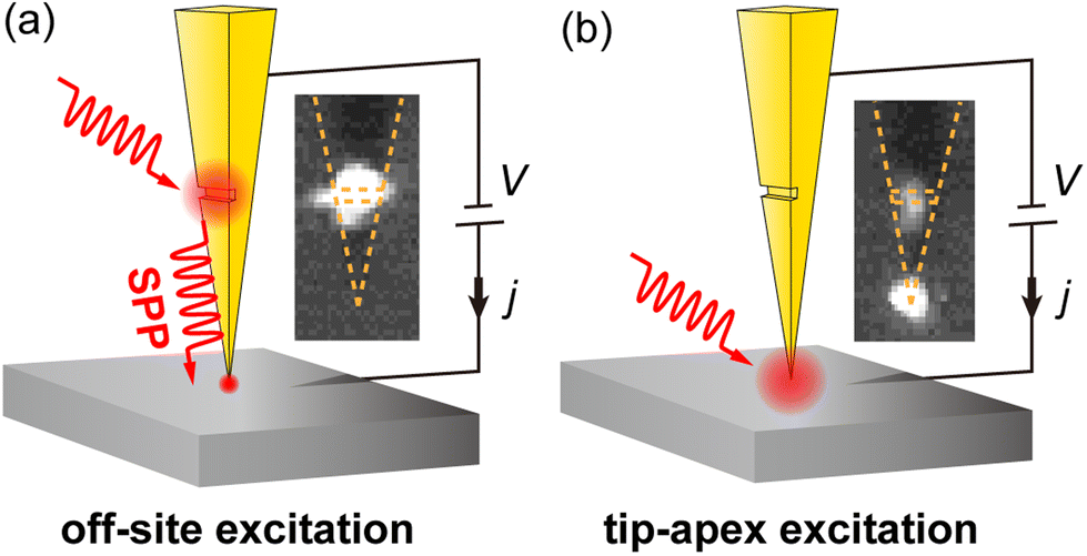 | ||
| Fig. 1 Schematic off-site (a) and tip-apex (b) excitation. Inset: optical image of light scattering under groove and apex illumination. | ||
While off-site excitation schemes employing SPP nanofocusing have been extensively explored in tip-enhanced optical spectroscopy based on atomic force microscopy under ambient conditions,16,20,21,23,31–36 their application in low-temperature STM for atomic-scale optical spectroscopy has only recently been initiated,37 and remains underdeveloped. While far-field background is not very critical in tip-enhanced Raman spectroscopy of submonolayer molecules38 or 2D materials39,40 on Au or Ag substrates, background scattering becomes a significant problem when conducting tip-enhanced photoluminescence spectroscopy of 2D materials41 and atomic-scale optical spectroscopy on the surface of bulk solids.42 In the latter case, the implementation of off-site excitation scheme in STM-based atomic-scale optical spectroscopy may be preferable. The off-site excitation scheme may also be advantageous to enhance sensitivity in elastic near-field scattering, which can suffer from interference with the background from far-field.42 In addition, efficient off-site excitation of the LSP in STM could be advantageous for ultrafast STM to reduce background photoemission currents and to enable the local optical excitation of the sample without large-scale sample illumination.
To evaluate SPP nanofocusing in low-temperature STM, an in situ evaluation method to quantitively compare the field enhancement generated by off-site versus tip-apex excitation of LSPs within the STM junction is needed. Two experimental approaches are available for this purpose: (1) detection of elastically or inelastically scattered light; (2) measuring photo-induced tunneling currents. Inelastic light scattering, such as tip-enhanced Raman spectroscopy, is often employed to evaluate the near-field intensity within STM junctions.16,43 In addition, photoemission current excited by femtosecond laser from free-standing nanotips44,45 or STM tips37,46 allows evaluation of the near-field intensity achieved by SPP nanofocusing.
Here, we introduce an additional approach for evaluating the field enhancement in plasmonic STM junctions using plasmon-assisted field emission resonances (FERs).47 This method offers a practical and reliable approach for in situ characterization of the near-field intensity during STM operation. Specifically, we demonstrate that it allows quantifying the relative field enhancement of direct tip-apex illumination versus off-site excitation of the LSP inside an Au-tip – Ag(111)-substrate junction. The intensity of the plasmon-assisted FERs, which are probed by highly localized tunneling current,47 serve as a sensitive probe for the near-field intensity inside the STM junction. Compared to photoemission currents,37,44–46 plasmon-assisted FERs are generated by one-photon absorption, i.e., a linear process, making it more accessible within the intensity range available in tip-enhanced Raman and photoluminescence spectroscopy.48 In contrast to previous studies which employed a grating coupler for off-site excitation and comparison of the resulting field enhancement with direct apex illumination,16,44 our work uses a single-groove coupler. This is a simplified version of a grating for sufficiently small laser spot sizes comparable to the groove size and has been employed to generate white “nanolight”.21 However, a direct comparison of the near-field enhancement achieved by a single-groove coupler with that of direct tip-apex illumination has not been carefully investigated.
2. Methods
Grooved tip design
Prior to tip fabrication, we conducted numerical simulations to examine the geometric parameters of the groove and pyramid shape of the tip shaft, aiming to maximize near-field enhancement at the tip apex under groove illumination. For simplicity, we use a free-standing tip without an Ag substrate in these parametric optimization studies. Fig. 2(a–c) illustrate the tip geometry, indicating five adjustable parameters: the distance between the groove edge and the tip apex (L), the width (W) and depth (D) of the groove, and the apex angles (θ1 and θ2). The value L of 10 μm ensures sufficient separation between the apex and the groove compared to the focal spot size of approximately 4 μm while minimizing damping of the SPP during propagation from the groove to the apex.14,49 By evaluating the field enhancement across different parameters, we obtain W = 900 nm, D = 300 nm, θ1 = 10° and θ2 = 20° as a nearly optimal combination. We chose the near optimal because we traded some field enhancement for easier fabrication. Fig. 2d shows an SEM of the tip fabricated by focused ion beam milling. The designed tip shape is well reproduced. More details about the tip design, simulation, and fabrication are described in the ESI section 1.† | ||
| Fig. 2 Design and fabrication of the grooved pyramid tip. (a–c) Structural parameters of the grooved pyramid tip; the red arrow indicates the central axis of the incident Gaussian beam. (d) SEM image of the fabricated tip. | ||
Experimental
The experiments were performed in a UHV chamber (base pressure <5 × 10⁻¹⁰ mbar) equipped with a low-temperature STM (modified UNISOKU USM-1400). The STM bias voltage (V) is applied to the Ag(111) sample and the tip is grounded. The Ag(111) surface was cleaned by repeated cycles of Ar+ sputtering and annealing up to 670 K, yielding an atomically flat surface. The UHV chamber has fused silica windows for optical access. A CW laser (633 nm or 780 nm) is focused on the STM junction at an angle of 55° with respect to the tip central axis using an in situ Ag-coated parabolic mirror mounted on the cryogenic STM stage. The diameter of the incident beam is around 5 mm, and the effective focal length of the parabolic mirror is 8.85 mm. Accurate beam alignment and focusing is achieved by piezo motors (Attocube GmbH) to position the parabolic mirror and to align three translational and two rotational axes. The laser is polarized along the plane spanned by the tip axis and the axis of the laser beam, and the diameter of the focal spot is estimated to be 6λ (where λ is the laser wavelength), which is estimated by scanning the focal spot across the tip apex and recording the distance over which the tip apex lights up. The movement of the parabolic mirror (and hence the laser spot) is calibrated from the known distance between the apex and the groove and the scattered light we observe from the junction (inset in Fig. 1).Turning the laser on or off causes thermal expansion of the tip, disturbing the measurements. To eliminate its impact, all measurements started several minutes after starting or stopping laser illumination, when thermal expansion is no longer detectable. The thermal expansion is monitored by measuring the tip height, i.e., change in the piezoelectric tube length, while maintaining a constant gap distance through the feedback loop. The differential conductance (∂j/∂V, with j the tunneling current) spectra are recorded using a lock-in amplifier with 20 mV modulation at a frequency of 983 Hz. All measurements are conducted at 15 K.
3. Results and discussion
The insets in Fig. 1 display optical images of light scattered from the groove and the tip-apex. As the laser focal spot is scanned along the tip axis, we observe two intensity maxima in the back-scattered light when the laser spot is at the apex and the groove, respectively. These maxima serve as indicators for precise positioning of the laser spot on the groove or the apex. In Fig. 1b, light scattering is observed from the groove when the tip apex is directly illuminated, indicating that SPPs propagate along the tip shaft and couple to the far-field at the groove. Conversely, the opposite behavior is expected when focusing the laser on the groove. However, strong back-reflection from the groove makes it challenging to observe the scattered light from the apex due to the limited dynamic range of the camera.
Fig. 3a shows ∂j/∂V spectra measured under dark conditions (gray) and during 780 nm laser illumination, for the laser being focused on the tip apex (blue curve) and the groove (red curve). In the constant-current mode (CCM) without illumination, we observed the first FER peak at 4.1 V, which corresponds to the image potential state on the Ag(111) surface.50 Off-site excitation with a 780 nm laser induces a shift in the first FER peak from its original position at V1 = 4.1 V to  , resulting in a difference of |ΔV1| = 1.5 V, where
  and V1 and
  represent the position of the first FER peak before and during laser illumination, respectively. The peak shift |ΔV1| = 1.5 V under off-site excitation is approximately equals to the incident photon energy of 1.59 eV. When the tip apex is illuminated directly, the first plasmon-assisted FER peak appears at
  , corresponding to a difference of |ΔV1| = 1.2 V relative to the original peak at V1 = 4.1 V, such that the |ΔV1| is smaller than the incident photon energy. The plasmon-assisted first FER peak arises from a resonant electron tunneling process in which an electron tunneling from the tip gains energy by absorption of a photon, such that it can tunnel into the image potential state at lower bias voltage.47 The different |ΔV1| between off-site and tip-apex illumination is attributed to an energetic shift of the image potential state due to different gap distances as explained in the ESI Fig. S3a.† Most importantly, we find that the plasmon-assisted first FER peak is stronger under off-site excitation than that under apex illumination, indicating that the near-field intensity is higher than that achieved with direct tip-apex illumination.
 | ||
| Fig. 3 (a and b). ∂j/∂V spectra acquired on Ag (111) surface under apex (blue) or groove (red) illumination showing FER peaks. The excitation wavelengths are 780 nm (hν = 1.59 eV) and 633 nm (hν = 1.96 eV), with the laser intensities at the focus are 9.6 kW cm−2 and 8.8 kW cm−2, respectively. The grey curves represent the spectra without illumination. The spectra in constant-current mode (CCM) were acquired with a current setpoint of 0.1 nA. The spectra in constant-gap-distance mode (CGM) were acquired with the gap distance set by a tunneling current of 0.1 nA at 1 V. The CGM spectra are shifted vertically for clarity. (c and e) ∂jph/∂V spectra acquired at constant gap distance set by a tunneling current of 0.1 nA at 1 V. (d and f) The ratios (orange dots) of ∂jph/∂V under groove to those under apex illumination. The solid lines indicate the average value. | ||
In CCM, the gap distance varies with bias voltage as well as different near-field intensity caused by off-site and tip-apex excitation (ESI Fig. S3†), as different bias voltage or near-field intensity result in different photocurrent assuming that the gap distance is constant. To ensure a fair comparison of the near-field intensities between the two excitation schemes, it is essential to measure and compare the FER spectra in constant gap-distance mode (CGM) and to maintain the same gap distance across different excitation configurations or across varying illuminating power. We employ the same STM setpoint for all FER measurements (e.g., V = 1 V and j = 0.1 nA) and verify that photocurrents are negligible at this setpoint, ensuring that the gap distance is determined by the static current after thermal equilibration of the electrons in metals (see ESI Fig. S4† for details). The ∂j/∂V spectra in Fig. 3a recorded in CGM show a slope with an onset at V ∼ 2.4 V during off-site and tip-apex excitation. The signal is again significantly higher under off-site excitation.
The data in Fig. 3b is measured at an excitation wavelength of 633 nm. In the CCM spectra, illumination causes a shift of the first FER peak by |ΔV1| = 1.8 V to  , with |ΔV1| closely matching the photon energy of 1.96 eV. In the CGM spectra, the plasmon-assisted FER peaks appear at a slightly higher voltage of
  , which we attribute to the energy shift of the image potential state caused by differences in gap distances between the CCM and CGM (ESI Fig. S3b† for details).
To quantitatively compare the near-field intensities of the LSPs excited by tip-apex and off-site excitation, the current in CGM can be expressed as
| j(V,|EA|) = jd(V) + jph(V,|EA|) = jd(V) + c1f1(V)|EA|2, | (1) |
 | (2) |
Therefore,  can be determined from the spectra in Fig. 3(a and b) recorded in CGM, which give
  and
and  for the illuminated and dark case, respectively.
  is plotted in Fig. 3(c and e). Denoting |EA| under groove and apex illumination as |EiGA| and |EiAA|, respectively, we derive the following relationship:
 | (3) |
This shows that the ratio of  measured under groove and tip-apex excitation equals the ratio of the local intensities,
  , and is independent of the bias voltage. Fig. 3(d and f) display the ratios plotted versus the bias voltage. The average ratios are indicated by the horizontal line. The data points are distributed randomly on both sides of the line, indicating that the ratio is indeed independent on the bias voltage, validating the relationship in eqn (3). We find that the average near-field intensity ratio is
  for the excitation wavelength of 780 nm and 1.7 for 633 nm. We also note that the oscillatory behavior of the ratio in Fig. 3f is due to noise from the lock-in amplifier (ESI Fig. S6†) and does not have any physical meaning.
The fact that the measured intensity ratio is greater than unity indicates that the energy flux directed into the LSP through off-site excitation surpasses that achieved by direct tip-apex excitation. The energy flux (SI unit: J s−1) refers to the rate of energy transfer through a surface (not per unit area). In the groove-coupled off-site excitation, a fraction of far-field energy flux is initially converted into propagating SPPs. During the nanofocusing process, the SPPs are damped by ohmic loss and radiating into the far-field, and some remaining energy is converted into LSPs creating a localized field inside the STM junction. The far- to near-field conversion efficiency is defined as the fraction of total incident energy flux that is directed into the near-field region inside the STM junction. Since the size of the near-field is the same under both excitation scheme, the ratio of conversion efficiency for off-site versus tip-apex excitation equals the ratio of the near-field intensity.16 The larger conversion efficiency observed for off-site excitation can be attributed to the larger geometric cross-section of the groove, fitting the size of laser focal spot better, and compensates for the additional SPP loss. Last, it worths mentioning that the intensity ratio of 3.8 at the excitation wavelength of 780 nm in this study is only slightly lower than the reported intensity ratio of 4.4 achieved for gratings at 785 nm wavelength.16‡
To further demonstrate the sensitivity of the intensity of the FER peak to the change of the near-field intensity, we examine the variation of plasmon-induced ∂jph/∂V signal as the laser focal spot is scanned along the tip axis (Fig. 4a). Fig. 4b displays the ∂j/∂V spectra in CGM obtained at various focal positions along the tip. The first plasmon-assisted FER peak at V = 2.5 V appears when the laser is focused on either the groove or the apex. Fig. 4c shows the resulting photocurrent and ∂jph/∂V(=∂j/∂V − djd/dV) at 2.5 V as a function of the focual position. The ∂jph/∂V spectra exhibit features of plasmon-assisted FER when the laser is focused on either the groove or the apex, but these features are absent when the focal spot is positioned between them. The plasmon-induced ∂jph/∂V, which directly reflects the near-field intensity in the junction, is sensitive to a change of the laser focual position of approximately 1 μm. This sensitivity suggests that the plasmon-assisted FER peak serves as a reliable indicator for precise optimization of the beam position on the tip.
 | ||
| Fig. 4 (a) Laser-spot positions for spectra acquisition along the tip axis. A SEM image of the tip is used for illustration purpose. The dashed circle illustrates the size of the focused beam. The purple dot means the laser spot at the mirror image of the tip (dashed outline). (b) ∂j/∂V spectra obtained at the focal positions marked in (a) with a 633 nm excitation wavelength. The spectra were recorded in the constant gap-distance mode at a gap distance set by V = 1 V and j = 0.1 nA. (c) ∂jph/∂V at V = 2.5 V as a function of focal position. | ||
To obtain further insights into the differences between the groove and apex illumination, we simulated the distributions of electric-field enhancement for both configurations. Fig. 5 presents the results for an excitation wavelength of 780 nm. The electric-field enhancement factor under groove (apex) illumination is defined as |EiG(A)A|/|Elaser|, where |Elaser| denote the electric-field amplitude of the incident laser at the center of the focal spot. Since |Elaser| is identical for both groove and apex illumination, the ratio of field enhancement factors is equivalent to the ratio of the electric-field amplitudes  . Fig. 5(a and b) compare the spatial distribution of the field enhancement along the surface of the pyramid tip. In the case of off-site excitation, a small fraction of the nanofocused SPPs reflects back from the apex and interferes with the counter-propagating SPPs along the shaft, forming weak interference fringes. In contrast, only weak SPP intensity and interference effects are observed for direct illumination of the tip apex, because the SPPs diverge, and their intensity decreases during propagating towards the groove. Fig. 5(c and d) show that the maximum field enhancement occurs at the atomic-scale protrusion under both groove and apex illumination. Notably, the field enhancement at the atomic-scale protrusion is significantly higher under groove illumination compared to apex illumination, further supporting the superior efficiency of groove-coupled off-site excitation in concentrating the field enhancement at the junction.
 | ||
| Fig. 5 Distributions of the enhancement factor under groove (a and c) and apex (b and d) illumination at an excitation wavelength of 780 nm. The incident wave vector (red arrow) is in the x–z plane and forms an angle of 35° with respect to the horizontal plane. | ||
Table 1 lists the field enhancement factors on the vacuum side of the tip apex under both off-site and tip-apex excitation. These values quantify the amplification of the electric field at the apex with the respective excitation schemes. The field enhancement factors reach several hundred within the gap formed between the tip and the Ag surface and are further amplified by approximately five-fold with the addition of an atomic-scale protrusion (picocavity) with both excitation schemes. At an excitation wavelength of 780 nm, the ratio of the near-field intensity under off-site excitation to that under tip-apex excitation is approximately 6.6, irrespective of the presence/absence of the atomic-scale protrusion. This confirms that the efficiency of groove-coupled off-site excitation of the LSP significantly surpasses that of direct tip-apex illumination. At the excitation wavelength of 633 nm, the simulated ratio of the near-field intensity for off-site versus tip-apex excitation decreases to approximately 4.6. The smaller value than that obtained for 780 nm is attributed to higher damping and ohmic loss for SPPs at higher frequencies.49 The experimental ratios in the last column of the table are lower than the simulated predictions, corresponding to approximately 39% and 57% of the simulated values at excitation wavelengths of 633 nm and 780 nm, respectively. This discrepancy arises from additional SPP scattering losses caused by surface roughness during nanofocusing in experiments, whereas the simulations assume an idealized, perfectly smooth pyramid surface with minimal scattering.
| λ (nm) | |EiGA|/|Elaser| | |EiAA|/|Elaser| | |EiGA|2/|EiAA|2 | |EiGA|2/|EiAA|2 |
|---|---|---|---|---|
| Simulation | Simulation | Simulation | Experiment | |
| The simulated enhancement factors without parentheses are taken from the vacuum side of the protrusions for tip apexes with atomic-scale protrusions, while the values in parentheses are from the vacuum side of the tip apexes without protrusions. | ||||
| 633 | 1218 (239) | 568 (108) | 4.6 (4.9) | 1.7 |
| 780 | 1426 (383) | 556 (148) | 6.6 (6.7) | 3.8 |
The exceptional performance of the grooved tip relies on careful optimization of its geometric parameters through simulations. Below, we outline this optimization process, focusing on the relationship between field enhancement at the tip apex and the grooved tip's geometry. Fig. 6(a–d) shows two-dimensional plots of the electric-field enhancement |EA|/|Elaser|, where |EA| is taken from the vacuum side of the tip apex. Fig. 6(a and b) explore various combinations of groove widths (W) ranging from 100 nm to 1000 nm and depths (D) ranging from 100 nm to 500 nm at the excitation wavelengths of 780 nm and 633 nm, respectively. The groove distance (L = 10 μm) and apex angles (θ1 = 10° and θ2 = 20°) are kept constant. The simulation results are in general agreement with a previous theoretical study on SPP excitation with a single groove,51 validating the approach and underlying principles of our analysis. At the excitation wavelength of 780 nm, the highest enhancement factors of 19.3 and 19.0 are obtained at W = 800 nm, D = 300 nm and W = 900 nm, D = 300 nm, respectively. At the excitation wavelength of 633 nm, the best enhancement factors of 8.1, 8.0, and 7.8 occur at W = 1000 nm, D = 200 nm, W = 1000 nm, D = 300 nm and W = 900 nm, D = 300 nm, respectively. Therefore, the combination of W = 900 nm and D = 300 nm is selected as it gives one of the best enhancements at both wavelengths.
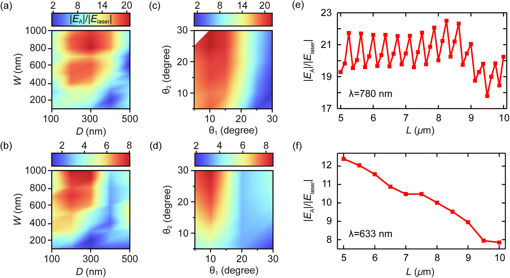 | ||
| Fig. 6 Enhancement factor of electric field at the tip apex as a function of (a and b) groove width W and depth D, (c and d) apex angles θ1 and θ2, and (e and f) groove-to-apex distance L. Fixed parameters: (a and b) θ1 = 10°, θ2 = 20°, and L = 10 μm. (c and d) W = 900 nm, D = 300 nm, and L = 10 μm. (e and f) θ1 = 10°, θ2 = 20°, W = 900 nm, and D = 300 nm. The excitation wavelength is 780 nm in (a, c and e) and 633 nm in (b, d and f). | ||
Next, the apex angles are optimized with fixed values of W = 900 nm and D = 300 nm. In general, the angle θ1 has a greater influence on the enhancement factor than θ2, as shown in Fig. 6(c and d). Decreasing θ1 enhances the nanofocusing effect,52 however, it also reduces groove's y-direction length (Ly), which in turn reduces the laser radiation received by the groove. At θ1 = 25°, the Ly becomes comparable to the diameter of the focused beam. Initially, as θ1 decreases, the enhancement factor increases because the enhanced adiabatic nanofocusing dominates. However, when θ1 drops below 10°, the reduction in the laser radiation received by the groove becomes dominant, leading to a decrease in the enhancement factor. The maximum enhancement factors are achieved at θ1 = 10°, θ2 = 25° and θ1 = 10°, θ2 = 30° for the excitation wavelengths of 780 nm and 633 nm, respectively. We select θ1 = 10° and θ2 = 20° because this combination is easier to fabricate due to a smaller difference between θ1 and θ2. The enhancement factor at θ1 = 10° and θ2 = 20° corresponds to approximately 90% of the maximum enhancement factor at both excitation wavelengths. In conclusion, we obtain W = 900 nm, D = 300 nm, θ1 = 10° and θ2 = 20° as a near-optimal combination.
As discussed above, the groove–apex distance (L) is fixed at 10 μm. Subsequently, we investigate the influence of L on the field enhancement at the tip apex, as shown in Fig. 6(e and f). At the excitation wavelength of 780 nm, the field enhancement oscillates with a periodicity of approximately λ/2 as L varies from 5 μm to 10 μm. This is attributed to the interference within the Fabry–Pérot cavity formed between the groove and the tip apex. Notably, the peak values of the oscillations remain nearly constant as L varies from 5 μm to 9 μm. In contrast, at the excitation wavelength of 633 nm, the field enhancement decays significantly as L varies from 5 μm to 10 μm. The observed difference between the two wavelengths arises from the different SPP decay lengths (LSPP). At 780 nm, the LSPP is substantially longer than L.53 As L increases, Ly increases, allowing the groove to capture more radiation to compensate for SPP losses. Conversely, at 633 nm, LSPP is comparable to L,53 causing SPP loss dominating as L increases. Therefore, the performance of the grooved tip can be further improved by reducing L.
4. Conclusions
In summary, we developed a novel method for comparing near-field intensity under different excitation schemes in an STM junction using plasmon-assisted FERs. We applied this approach to evaluate the field enhancement of a plasmonic picocavity in a low-temperature STM, resulting from an off-site excitation via plasmonic nanofocusing. We fabricated a grooved pyramid tip with nearly optimized geometric parameters that are W = 900 nm, D = 300 nm, θ1 = 10° and θ2 = 20° and quantified ratio of near-field intensity at the tip apex under off-site excitation relative to that under direct tip-apex excitation. At an excitation wavelength of 780 nm, the ratio of the near-field intensities under groove and apex illumination is close to 3.8, reaching 57% of the theoretical value. At the excitation wavelength of 633 nm, the ratio is 1.7, which corresponds to 38% of the theoretical value but is still greater than unity. These suggest that the grooved pyramidal tip is suitable for multi-wavelength excitations. Prospectively, the grooved pyramidal tip offers a relatively simple structure for tip-enhanced optical spectroscopy by effectively suppressing the significant far-field contributions, paving the way for more precise and background-free near-field spectroscopic studies.Author contributions
Chenfang Lin: investigation; methodology (equal); formal analysis (equal); supervision (equal); writing – review & editing (equal). Jie Li: formal analysis (equal); writing – original draft (equal). Guoao Li: methodology (equal). Wenjie Luo: writing – original draft (equal). Shuyi Liu: resources (equal). Adnan Hammud: resources (equal). Yang Xia: resources (equal). Anlian Pan: resources (equal). Martin Wolf: resources (equal). Melanie Müller: writing – review & editing (auxiliary); supervision (equal). Takashi Kumagai: conceptualization; funding acquisition; supervision (equal); writing – review & editing (equal).Data availability
Data for this article are available at Zenodo at https://doi.org/10.5281/zenodo.14600345.Conflicts of interest
There are no conflicts to declare.Acknowledgements
The authors thank Hiroko Yoshino for supporting the experiments. T. K. acknowledges a support by JST FOREST Program (Grant Number JPMJFR201J, Japan). C. L. acknowledges the support by the National Key Research and Development Program of China (No. 2022YFA1204700), the National Natural Science Foundation of China (No. 12104146), the Natural Science Foundation of Hunan Province (No. 2022JJ20002), and the Fundamental Research Funds for the Central Universities (No. 227202101005, 227202201293).References
- R. Gutzler, M. Garg, C. R. Ast, K. Kuhnke and K. Kern, Nat. Rev. Phys., 2021, 3, 441–453 CrossRef
.
- R. Zhang, Y. Zhang, Z. C. Dong, S. Jiang, C. Zhang, L. G. Chen, L. Zhang, Y. Liao, J. Aizpurua, Y. Luo, J. L. Yang and J. G. Hou, Nature, 2013, 498, 82–86 CrossRef CAS PubMed
- J. Lee, K. T. Crampton, N. Tallarida and V. A. Apkarian, Nature, 2019, 568, 78–82 CrossRef CAS PubMed
- B. Yang, G. Chen, A. Ghafoor, Y. Zhang, Y. Zhang, Y. Zhang, Y. Luo, J. Yang, V. Sandoghdar, J. Aizpurua, Z. Dong and J. G. Hou, Nat. Photonics, 2020, 14, 693–699 CrossRef CAS
- M. Imai-Imada, H. Imada, K. Miwa, Y. Tanaka, K. Kimura, I. Zoh, R. B. Jaculbia, H. Yoshino, A. Muranaka, M. Uchiyama and Y. Kim, Nature, 2022, 603, 829–834 CrossRef CAS PubMed
- J. Y. Xu, X. Zhu, S. J. Tan, Y. Zhang, B. Li, Y. Z. Tian, H. Shan, X. F. Cui, A. D. Zhao, Z. C. Dong, J. L. Yang, Y. Luo, B. Wang and J. G. Hou, Science, 2021, 371, 818–822 CrossRef CAS PubMed
- Y. Park, I. Hamada, A. Hammud, T. Kumagai, M. Wolf and A. Shiotari, Nat. Commun., 2024, 15, 6709 CrossRef CAS PubMed
- Q. Meng, J. Zhang, Y. Zhang, W. Chu, W. Mao, Y. Zhang, J. Yang, Y. Luo, Z. Dong and J. G. Hou, Sci. Adv., 2024, 10, eadl1015 CrossRef CAS PubMed
- B. Cirera, M. Wolf and T. Kumagai, ACS Nano, 2022, 16, 16443–16451 CrossRef CAS PubMed
- F. Benz, M. K. Schmidt, A. Dreismann, R. Chikkaraddy, Y. Zhang, A. Demetriadou, C. Carnegie, H. Ohadi, B. de Nijs, R. Esteban, J. Aizpurua and J. J. Baumberg, Science, 2016, 354, 726–729 CrossRef CAS PubMed
- J. J. Baumberg, Nano Lett., 2022, 22, 5859–5865 CrossRef CAS PubMed
- M. Urbieta, M. Barbry, Y. Zhang, P. Koval, D. Sanchez-Portal, N. Zabala and J. Aizpurua, ACS Nano, 2018, 12, 585–595 CrossRef CAS PubMed
- T. L. Vasconcelos, B. S. Archanjo, B. Fragneaud, B. S. Oliveira, J. Riikonen, C. Li, D. S. Ribeiro, C. Rabelo, W. N. Rodrigues, A. Jorio, C. A. Achete and L. G. Cancado, ACS Nano, 2015, 9, 6297–6304 CrossRef CAS PubMed
- H. Bockmann, M. Muller, A. Hammud, M. G. Willinger, M. Pszona, J. Waluk, M. Wolf and T. Kumagai, J. Phys. Chem. Lett., 2019, 10, 2068–2074 CrossRef PubMed
- F. Lu, W. Zhang, M. Liu, L. Zhang and T. Mei, IEEE J. Sel. Top. Quantum Electron., 2021, 27, 1–12 Search PubMed
- S. Berweger, J. M. Atkin, R. L. Olmon and M. B. Raschke, J. Phys. Chem. Lett., 2010, 1, 3427–3432 CrossRef CAS
- A. J. Babadjanyan, N. L. Margaryan and K. V. Nerkararyan, J. Appl. Phys., 2000, 87, 3785–3788 CrossRef CAS
- M. I. Stockman, Phys. Rev. Lett., 2004, 93, 137404 CrossRef PubMed
- C. Ropers, C. C. Neacsu, T. Elsaesser, M. Albrecht, M. B. Raschke and C. Lienau, Nano Lett., 2007, 7, 2784–2788 CrossRef CAS PubMed
- S. Berweger, J. M. Atkin, R. L. Olmon and M. B. Raschke, J. Phys. Chem. Lett., 2012, 3, 945–952 CrossRef CAS PubMed
- T. Umakoshi, M. Tanaka, Y. Saito and P. Verma, Sci. Adv., 2020, 6, eaba4179 CrossRef CAS PubMed
- C. C. Neacsu, S. Berweger, R. L. Olmon, L. V. Saraf, C. Ropers and M. B. Raschke, Nano Lett., 2010, 10, 592–596 CrossRef CAS PubMed
- K. Zhang, S. I. Taniguchi and T. Tachizaki, Opt. Lett., 2018, 43, 5937–5940 CrossRef CAS PubMed
- K. V. Nerkararyan, Phys. Lett. A, 1997, 237, 103–105 CrossRef CAS
- D. K. Gramotnev and S. I. Bozhevolnyi, Nat. Photonics, 2013, 8, 13–22 CrossRef
- M. Esmann and C. Lienau, Microsc. Anal., 2020, 47, 22–23 Search PubMed
- D. Xu, B. Liang, Y. Xu and M. Liu, Nano Res., 2022, 16, 5555–5571 CrossRef
- A. Wöste, G. Hergert, T. Quenzel, M. Silies, D. Wang, P. Groß and C. Lienau, Nano Lett., 2023, 23, 5528–5534 CrossRef PubMed
- W. Luo, R. Song, B. G. Whetten, D. Huang, X. Cheng, A. Belyanin, T. Jiang and M. B. Raschke, Small, 2024, 20, 2307345 CrossRef CAS PubMed
- W. Luo, B. G. Whetten, V. Kravtsov, A. Singh, Y. Yang, D. Huang, X. Cheng, T. Jiang, A. Belyanin and M. B. Raschke, Nano Lett., 2023, 23, 1767–1773 CrossRef CAS PubMed
- T. Jiang, V. Kravtsov, M. Tokman, A. Belyanin and M. B. Raschke, Nat. Nanotechnol., 2019, 14, 838–843 CrossRef CAS PubMed
- T. Umakoshi, Y. Saito and P. Verma, Nanoscale, 2016, 8, 5634–5640 RSC
- K. Tomita, Y. Kojima and F. Kannari, Nano Lett., 2018, 18, 1366–1372 CrossRef CAS PubMed
- X. Ma, Y. Zhu, N. Yu, S. Kim, Q. Liu, L. Apontti, D. Xu, R. Yan and M. Liu, Nano Lett., 2019, 19, 100–107 CrossRef CAS PubMed
- K. Zhang, Y. Bao, M. Cao, S.-I. Taniguchi, M. Watanabe, T. Kambayashi, T. Okamoto, M. Haraguchi, X. Wang, K. Kobayashi, H. Yamada, B. Ren and T. Tachizaki, Anal. Chem., 2021, 93, 7699–7706 CrossRef CAS PubMed
- V. Kravtsov, R. Ulbricht, J. M. Atkin and M. B. Raschke, Nat. Nanotechnol., 2016, 11, 459–464 CrossRef CAS PubMed
- G. A. Traeger, M. H. Teichmann, B. Schröder and M. Wenderoth, Rev. Sci. Instrum., 2023, 94, 023702 CrossRef CAS PubMed
- B. Pettinger, P. Schambach, C. J. Villagomez and N. Scott, Annu. Rev. Phys. Chem., 2012, 63, 379–399 CrossRef CAS PubMed
- A. Shiotari, T. Kumagai and M. Wolf, J. Phys. Chem. C, 2014, 118, 11806–11812 CrossRef CAS
- H. An, J. Li, Y. Liu, P. Xu, S. Han, Y. Liu, S. Chen, S.-Y. Li, C. Lin and A. Pan, J. Phys. Chem. C, 2024, 128, 7583–7590 CrossRef CAS
- K.-D. Park, O. Khatib, V. Kravtsov, G. Clark, X. Xu and M. B. Raschke, Nano Lett., 2016, 16, 2621–2627 CrossRef CAS PubMed
- A. Shiotari, J. Nishida, A. Hammud, F. Schulz, M. Wolf, T. Kumagai and M. Müller, arXiv, 2024, preprint, arXiv:2410, p. 18455, DOI:10.48550/arXiv.2410.18455.
- S. Liu, F. P. Bonafe, H. Appel, A. Rubio, M. Wolf and T. Kumagai, ACS Nano, 2023, 17, 10172–10180 CrossRef CAS PubMed
- M. Müller, V. Kravtsov, A. Paarmann, M. B. Raschke and R. Ernstorfer, ACS Photonics, 2016, 3, 611–619 CrossRef
- J. Vogelsang, J. Robin, B. J. Nagy, P. Dombi, D. Rosenkranz, M. Schiek, P. Gross and C. Lienau, Nano Lett., 2015, 15, 4685–4691 CrossRef CAS PubMed
- B. Schröder, O. Bunjes, L. Wimmer, K. Kaiser, G. A. Traeger, T. Kotzott, C. Ropers and M. Wenderoth, New J. Phys., 2020, 22, 033047 CrossRef
- S. Liu, M. Wolf and T. Kumagai, Phys. Rev. Lett., 2018, 121, 226802 CrossRef CAS PubMed
- X.-B. Zhang, Y.-F. Zhang, H. Li, J. Cui, S. Jiang, B. Yang, Y. Zhang, Y. Zhang and Z.-C. Dong, Chin. J. Chem. Phys., 2022, 35, 713–719 CrossRef CAS
- H. Bockmann, S. Liu, M. Muller, A. Hammud, M. Wolf and T. Kumagai, Nano Lett., 2019, 19, 3597–3602 CrossRef PubMed
- T. Kumagai, S. Liu, A. Shiotari, D. Baugh, S. Shaikhutdinov and M. Wolf, J. Phys.: Condens. Matter, 2016, 28, 494003 CrossRef CAS PubMed
- J. Renger, S. Grafström and L. M. Eng, Phys. Rev. B: Condens. Matter Mater. Phys., 2007, 76, 045431 CrossRef
- R. Yadav, T. Umakoshi and P. Verma, AIP Adv., 2022, 12, 085216 CrossRef CAS
- M. Kuttge, E. J. R. Vesseur, J. Verhoeven, H. J. Lezec, H. A. Atwater and A. Polman, Appl. Phys. Lett., 2008, 93, 113110 CrossRef
Footnotes |
| † Electronic supplementary information (ESI) available. See DOI: https://doi.org/10.1039/d4nr04262j |
| ‡ The TERS intensity is proportional to the fourth power of the electric-field amplitude, so we determined the near-field intensity ratio between grating and apex illumination to be approximately 4.4 after taking the square root of the ratio of TERS intensities, which is approximately 20 in the reference. |
| This journal is © The Royal Society of Chemistry 2025 |