
 Open Access Article
 This Open Access Article is licensed under a Creative Commons Attribution-Non Commercial 3.0 Unported Licence
∼5-Fold enhancement in the thermoelectric figure of merit of sustainable 3D-CuNi interconnected nanonetworks due to ultralow lattice thermal conductivity†
Cristina V.
Manzano
 *a,
Olga
Caballero-Calero
a,
Daniele
Casari
b,
Amit
Sharma
b,
Alba
Díaz-Lobo
a,
Xavier
Maeder
b and
Marisol
Martín-González
a
*a,
Olga
Caballero-Calero
a,
Daniele
Casari
b,
Amit
Sharma
b,
Alba
Díaz-Lobo
a,
Xavier
Maeder
b and
Marisol
Martín-González
a
aInstituto de Micro y Nanotecnología, IMN-CNM, CSIC (CEI UAM+CSIC) Isaac Newton, 8, E-28760, Tres Cantos, Madrid, Spain. E-mail: cristina.vicente@csic.es
bEmpa, Swiss Federal Laboratories for Materials Science and Technology, Laboratory for Mechanics of Materials and Nanostructures, Feuerwerkerstrasse 39, CH-3602 Thun, Switzerland
First published on 3rd February 2025
Abstract
The pursuit of efficient thermoelectric materials, particularly those composed of low-toxicity and Earth-abundant elements, has intensified in recent years. This study introduces an approach to increase the thermoelectric properties of CuNi alloys through the synergistic application of two nanostructuring techniques: the incorporation of saccharine into the electrolyte to achieve a crystallite size reduction to 23–26 nm and the utilization of three-dimensional (3D) anodic aluminum oxide (3D-AAO) templates to fabricate nanowire networks. For comparison purposes, we successfully electrodeposited CuNi films, one-dimensional (1D) nanowire arrays, and modulated nanowire arrays, together with 3D-nanonetworks, maintaining a consistent composition of Cu0.60Ni0.40 across all samples. Notably, while the electrical conductivity and Seebeck coefficient remained consistent between the nanocrystalline CuNi films and the 3D-nanonetworks, a significant reduction in thermal conductivity was observed, decreasing from 29 W m−1 K−1 for the bulk material to 10.9 ± 1.1 W m−1 K−1 for nanocrystalline films, to 5.3 ± 0.5 W m−1 K−1 for the 3D nanonetworks, and to 4.9 ± 0.6 W m−1 K−1 for free-standing 3D CuNi nanonetworks. This reduction is attributed to enhanced phonon scattering within the 3D architecture together with the nanocrystalline size inside the nanowires. The figure of merit (zT) exhibited an impressive increase of more than four times (4.4) for 3D-CuNi nanonetworks within AAO templates and 4.8 times for free-standing 3D-CuNi nanonetworks, when compared to bulk. Our findings underscore the potential of dual nanostructuring strategies to optimize the thermoelectric performance of environmentally friendly, stable, and abundant materials like CuNi, paving the way for advancements in sustainable energy technologies.
1. Introduction
Increasing reliance on conventional energy sources such as natural gas, petroleum, and coal has led to a significant rise in global temperatures, contributing to the pressing issue of climate change. In response to this environmental crisis, extensive research efforts have been directed towards the development of alternative energy solutions that are not only efficient but also sustainable. A critical area of focus within this field is the advancement of thermoelectric materials that are both non-toxic and composed of Earth-abundant elements.1 These materials have the unique ability to convert thermal gradients into electrical voltage and vice versa, thus playing a key role in energy conversion technologies. The efficiency of thermoelectric materials is assessed quantitatively using the figure of merit (zT), defined by the following equation: | (1) |
In recent years, CuNi alloys have attracted considerable attention as promising candidates for thermoelectric applications due to their very high electrical conductivity and a moderate Seebeck coefficient, even though they have a very high thermal conductivity.3 CuNi alloys show very good values as power thermoelectric generators4 and giant Peltier coolers.5 Various strategies have been explored to improve the thermoelectric performance of these alloys, in particular by reducing the thermal conductivity. Doping with elements such as tin and tungsten has enabled a small decrease in thermal conductivity from 18 W m−1 K−1 to 16 W m−1 K−1 at RT,6 while the incorporation of SiO2 particles into a Cu55Ni45 matrix has achieved reductions to 16 W m−1 K−1 (ref. 7) at 300 K. In addition, selenium doping and the introduction of carbon nanotubes have been shown to significantly reduce the thermal conductivity from 48.1 to 9.6 W m−1 K−1 at temperatures as high as 873 K.8
Nanostructuring is a well-established method for enhancing the thermoelectric properties of materials, in particular through enhanced phonon scattering that occurs at the surfaces and interfaces of nanostructures.9,10 Our previous work demonstrated a significant reduction in thermal conductivity from 30 W m−1 K−1 for bulk materials to 9 ± 0.9 W m−1 K−1 for nanocrystalline Cu0.55Ni0.45 films,11 achieved by the addition of saccharine during electrodeposition, which effectively reduced the crystallite size to 30–40 nm.12–14
In this study, we aim to combine two different strategies for the nanostructuring of CuNi alloys: the growth of nanocrystalline CuNi by the addition of saccharine to the electrolyte and the fabrication of various nanostructured forms—including 1D-nanowire arrays, modulated nanowire arrays, and 3D-nanonetworks—using anodic aluminum oxide (AAO) for template-assisted electrochemical deposition. This research aims to eliminate the contribution of phonons to thermal conductivity by combining these two nanostructuring methods using an economical and scalable fabrication approach such as electrodeposition. The crystallographic structure, composition, and morphology of the resulting CuNi films and nanostructures will be analyzed, as well as their thermoelectric properties, including electrical conductivity, Seebeck coefficient, and thermal conductivity. The ultimate goal is to assess the influence of reduced dimensions on the thermoelectric efficiency of CuNi alloys, thereby contributing to the development of non-toxic, Earth-abundant materials suitable for small-sized thermoelectric generators.
2. Experimental methods
2.1. Fabrication of one-dimensional (1D), modulated, and three-dimensional (3D) anodic aluminum oxide (AAO) templates
The fabrication process for the AAO templates involves a common initial step followed by specific steps for each template type. All templates were fabricated using a two-step anodization process with the following parameters: an electrolyte of 0.3 M H2SO4, an applied voltage of 25 V, and a temperature of 0 °C. The first anodization time was 24 hours. For 1D-AAO templates, the second step anodization15 was carried out with the same electrolyte, applied voltage, and temperature16 as the first one for 9 hours to obtain a thickness of approximately 40 μm. After anodization, chemical etching with 5 wt% H3PO4 at 30 °C for 20 min was performed to increase the pore diameter.For modulated-AAO and 3D-AAO templates, after the initial anodization, the second anodization step consisted of pulsed anodization alternating between mild (25 V for 180 s) and hard anodization (33 V for 2 s) conditions.17–19 The number of pulses was 60, corresponding to 15 μm of 3D-AAO, while the other 25 μm corresponded to 1D-AAO to obtain a total thickness of 40 μm. To obtain the modulated-AAO and 3D-AAO templates, chemical etching with 5 wt% H3PO4 at 30 °C was performed for 18 min for modulated-AAO and 23 min for 3D-AAO.17–19
For the three templates used in this study, 1D-AAO, modulated-AAO and 3D-AAO, the aluminum substrate was removed using an aqueous solution of CuCl2 and HCl and the barrier layer was opened using an aqueous solution of 10 wt% H3PO4 for 10 min at 30 °C.
2.2. Electrodeposition of CuNi films and 1D-, modulated- and 3D-CuNi nanostructures
CuNi films were deposited onto Si substrates coated with a layer of electron-beam deposited Cr (5 nm) and Au (150 nm) to form the conductive working electrode for the subsequent electrochemical deposition. Then, to perform the electrodeposition of the 1D-, modulated-, and 3D-CuNi nanostructures inside the different AAO templates, 150 nm of Au and 5 nm of Cr were first deposited on one of the sides of the templates to have the electrical contact necessary to form the working electrode required for the electrodeposition.The electrolyte used was an aqueous solution of 0.3 M NiSO4·6H2O (98%, Sigma-Aldrich), 0.08 M CuSO4·5H2O (99%, Sigma-Aldrich), 0.2 M sodium citrate (C6H5Na3O7·2H2O (99%, Sigma-Aldrich)), 0.7 mM sodium dodecyl sulfate (SDS (97%, Sigma-Aldrich)) and 10.9 mM saccharine (99%, Sigma-Aldrich).14 Sodium citrate was used as a complexing agent, saccharine to reduce the grain size of the alloy, and sodium dodecyl sulfate (SDS) as a wetting agent.12 It was necessary to keep the pH of the solution at 6 to avoid the precipitation of copper during the electrodeposition.20
All the CuNi nanostructures were electrodeposited using a vertical electrochemical cell with three electrodes: the working electrode was the 150 nm Au/5 nm Cr/AAO template (or Si in the case of films) described above, the counter electrode was a Pt mesh, and the reference electrode was Ag/AgCl. The electrodeposition temperature was controlled using an electrochemical cell with a double-walled jacket and maintained in this case at 45 ± 1 °C. A potentiostat-galvanostat (Eco Chemie, model AUT302) from Metrohm Autolab was used. Pulsed galvanostatic deposition was performed between a current density of −60 mA cm−2 for 0.3 s and zero current density for 3 s for 4 hours to obtain a uniform composition and uniform growth rate of the CuNi nanostructures.
After electrodeposition, Cr was removed using an aqueous solution of 0.25 M KMnO4 and 0.5 M NaOH at room temperature for a few seconds, and Au was removed using an Au etchant (from Sigma-Aldrich, Ni compatible) for a few seconds. In addition, a CuNi film was electrodeposited under the same conditions for 4 h and characterized for comparison with the CuNi nanostructures.
2.3. Structural, compositional, and morphological characterization of CuNi films and 1D-, modulated- and 3D-CuNi nanostructures
The structural characterization of the CuNi nanostructures was carried out by high-resolution X-ray diffraction (XRD); these measurements were performed in a Philips X'Pert four-circle diffractometer system in the Bragg–Brentano configuration with CuKα radiation. The degree of preferred orientation was quantified by Harris texture analysis21 according to the following equation: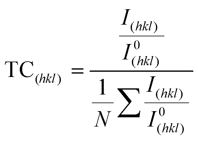 | (2) |
 | (3) |
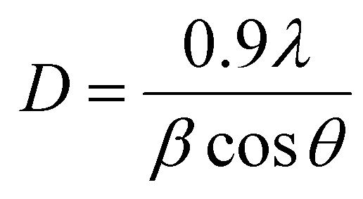
Saccharine is added to the CuNi electrolyte to obtain nanocrystalline alloys. To determine if the CuNi alloys are nanocrystalline, the crystallite size in the (111) diffraction peak was calculated using the Scherrer equation:
 | (4) |
The morphological characterization of the cross-section of the CuNi nanostructures was performed using a field emission-scanning electron microscope (FE-SEM, FEI VERIOS 460) with an accelerating voltage of 2 kV. The morphological characterization of the CuNi nanostructures was carried out both inside the AAO templates and after the removal of the porous alumina. The alumina was removed using an aqueous solution of phosphoric acid (7 wt%) and chromic oxide (1.8 wt%), in which the nanostructures were immersed at 45 °C for two days. This solution was then filtered with ethanol under vacuum conditions to collect the nanostructures. The filter was immersed in a small flask of ethanol to disperse the nanostructures in the solution. Finally, this solution was carefully pipetted to avoid bent or twisted nanowires on a carbon grid to obtain dispersed nanostructures. Energy-dispersive X-ray (EDX) was used to study the uniformity of the composition along the cross-section of the CuNi nanostructures using an S-3000 N EDX with an acceleration voltage of 20 kV.
The crystal structures of the films and of the nanostructures were also evaluated using both transmission Kikuchi diffraction (TKD) and precession electron diffraction (PED). TKD measurements were performed using a Lyra dual-beam SEM-FIB (focused ion beam) instrument (TESCAN) at 30 kV and 10 nA, with step sizes of 5–15 nm. PED measurements were performed using a Themis 200 G3 aberration (probe) corrected TEM (Thermo Fisher) equipped with a NanoMEGAS ASTAR system. Orientation maps along the film cross-section were acquired at 200 kV using a precession angle of 0.6° and a step size of 4 nm.
2.4. Thermoelectric properties of CuNi films and 1D-, modulated- and 3D-CuNi nanostructures
The electrical conductivity, σ, and the Seebeck coefficient, S, of the films and 3D-CuNi nanonetworks were measured in-plane at room temperature. For these measurements, contacts were placed on the top of the films and 3D-nanonetworks. The electrical conductivity values were measured using a commercial Hall Ecopia HMS-5500 system, while the Seebeck coefficient was measured using a home-made system. The experimental errors associated with these thermoelectric properties were 5% and 10% for the electrical conductivity and Seebeck coefficient, respectively. From these two parameters, σ and S, the power factor, PF, was calculated using PF = σ·S2. It is important to note that these two parameters were not measured for 1D-CuNi nanowires and modulated-CuNi nanowires, as there is no electrical connection between the nanowires in the in-plane direction.COMSOL Multiphysics software was used to model the effective electrical conductivity of the 3D-CuNi nanonetworks. A geometry consisting of 69 nanowires with a diameter of 50 nm, an interpore distance of 69 nm and a length of 1800 nm with a hexagonal arrangement was established. Each nanowire was connected with transversal channels to its first neighbors, forming a structure similar to the experimental one, of a 3D-CuNi network with a period of 180 nm. The material properties were taken from the COMSOL library. To simulate the steady state electrical potential, a potential difference was imposed between two nanowire terminals, to mimic the experimental procedure of the electrical conductivity measurement (see Fig. S1 in the ESI,† where the independence of the used mesh in the obtained simulations is shown).
The out-of-plane thermal diffusivity was measured at room temperature using the photoacoustic (PA) technique, as in the other studies on electrodeposited materials by our group.22,23 The thermal conductivity, k, was then calculated using the density, ρ, and the specific heat, Cp, which depend on the CuNi film or nanostructure, using the following equation: k = α·ρ·Cp.24 This technique is based on the detection of the phase shift between two signals using a lock-in amplifier. The first signal is a laser pulse (Alphalas modulated fiber-coupled laser, with 980 nm wavelength and 260 mW intensity) that periodically heats the surface of the film or nanostructure, which has been previously coated with an 80 nm titanium layer; and the second one is the acoustic signal generated by the expansion and contraction of the air in contact with the surface of the film or nanostructure, which is detected using a microphone (40 BL 1/4′′ CCP pressure type, with a 26 CB, 1/4′′ preamplifier, both from G.R.A.S. Sound & Vibration). This phase shift is compared with the one obtained by performing the same experiment on a reference signal (a quartz substrate, also coated with 80 nm of titanium to act as a transducer). Knowing these phase shifts and using the multilayer model developed by Hu et al.,25 the thermal diffusivity, α, of the film or nanostructure can be obtained. The error of the thermal conductivity measurements using the PA technique is approximately 10%.26,27
3. Results and discussion
The crystallographic structure of the electrodeposited CuNi films and nanostructures (1D-, modulated, and 3D-) was analyzed by X-ray diffraction (XRD) measurements. The resulting diffractograms, shown in Fig. 1, reveal three distinct diffraction peaks corresponding to the cubic structure of CuNi (JCPDS 09-0205). These diffraction peaks are identified as (111), (200), and (220). Notably, the presence of Au diffraction peaks in the AAO diffractogram indicates the back coating of the AAOs used for the electrodeposition.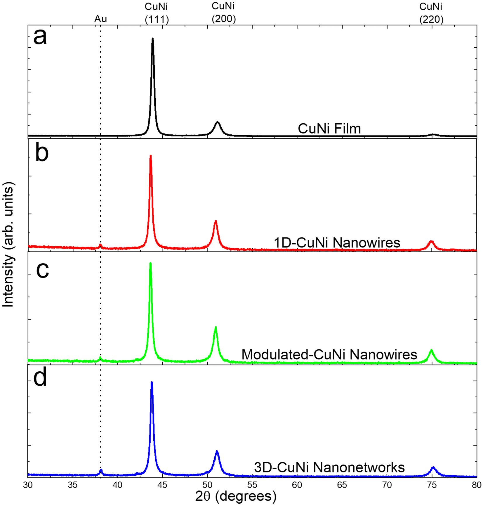 | ||
| Fig. 1 X-ray diffractograms of (a) the CuNi film, (b) 1D-CuNi nanowires, (c) modulated-CuNi nanowires, and (d) 3D-CuNi nanonetworks. | ||
The degree of preferred orientation was analyzed quantitatively using the texture coefficient as summarized in Table 1. The analysis shows that all samples exhibit polycrystalline characteristics. The CuNi film is highly textured along the [111] direction, while the 1D-CuNi nanowires, modulated-CuNi nanowires and 3D-CuNi nanonetworks are oriented along the [111] direction, but the presence of [200] and [220] directions must also be considered.
| Material | Peak (hkl) | Intensity XRD | Intensity JCPDS | Texture coefficient (TC(hkl)) | Standard deviation (σTC) | FWHM (111) | Crystallite size (nm) |
|---|---|---|---|---|---|---|---|
| Film | 111 | 22.05 | 100 | 2.11 | 0.82 | 0.38 | 23 ± 1 |
| 200 | 3.30 | 45 | 0.70 | ||||
| 220 | 0.44 | 23 | 0.18 | ||||
| 1D-CuNi nanowires | 111 | 5.09 | 100 | 1.37 | 0.29 | 0.34 | 25 ± 1 |
| 200 | 1.62 | 45 | 0.97 | ||||
| 220 | 0.56 | 23 | 0.66 | ||||
| Modulated-CuNi nanowires | 111 | 4.51 | 100 | 1.21 | 0.18 | 0.33 | 26 ± 1 |
| 200 | 1.67 | 45 | 1.00 | ||||
| 220 | 0.67 | 23 | 0.78 | ||||
| 3D-CuNi nanonetworks | 111 | 5.91 | 100 | 1.43 | 0.31 | 0.37 | 23 ± 1 |
| 200 | 1.66 | 45 | 0.89 | ||||
| 220 | 0.65 | 23 | 0.68 |
The crystallite size was calculated using the (111) diffraction peak and the Scherrer equation. The crystallite sizes were 23 ± 1 nm, 25 ± 1 nm, 26 ± 1 nm, and 23 ± 1 nm for the CuNi films, 1D-CuNi nanowires, modulated-CuNi nanowires, and 3D-CuNi nanonetworks, respectively, confirming the nanocrystalline nature of all the morphologies studied.
The compositional analysis of the CuNi film and nanostructures was performed using energy dispersive X-ray (EDX) along the cross-section of the samples to verify that it was uniform along the thickness. The composition was determined to be Cu0.61Ni0.39 for the films and Cu0.59Ni0.41, Cu0.59Ni0.41, and Cu0.61Ni0.39, for 1D-CuNi nanowires, modulated-CuNi nanowires, and 3D-CuNi nanonetworks, respectively. Considering the 5% error associated with the EDX composition determination, these results indicate that the compositions are within the experimental error for the different films and nanostructures.
Fig. 2 shows the orientation mapping and scanning electron microscopy (SEM) images of the CuNi film and CuNi nanostructures (1D nanowires, modulated nanowires, and 3D nanonetworks). Due to the nanocrystalline nature of the films, the morphology was not visible in the SEM images. However, precision electron diffraction (PED) analysis confirms the polycrystalline structure of the CuNi film, with a predominant crystallographic orientation of [111], consistent with the XRD results. The average grain size obtained from PED is 16 nm.
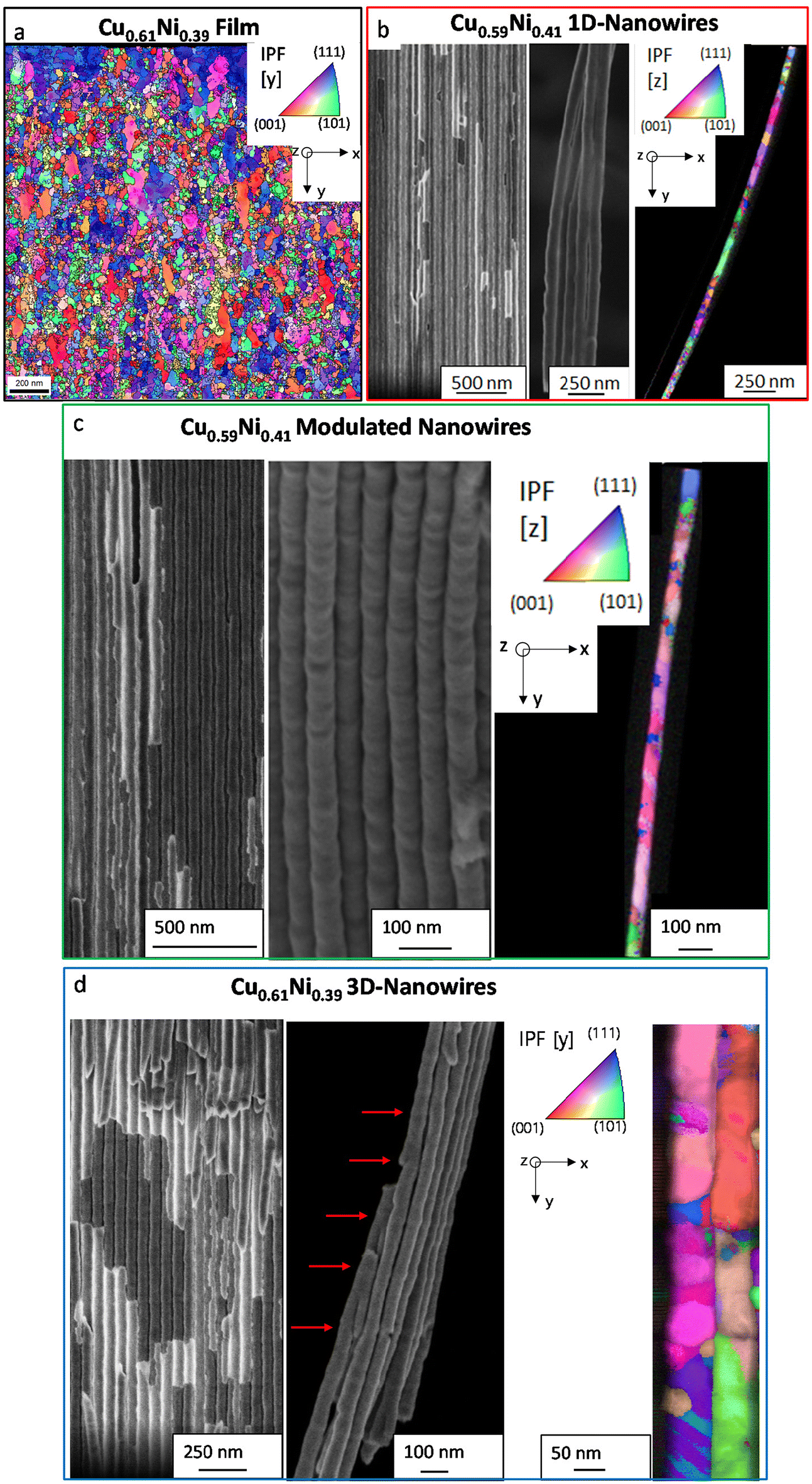 | ||
| Fig. 2 (a) PED orientation mapping of the CuNi film, SEM images inside AAO templates and after dissolving the AAO and transmission Kikuchi diffraction (TKD) images of (b) 1D-CuNi nanowires, (c) modulated-CuNi nanowires, and (d) 3D-CuNi nanonetworks both inside and outside the 3D-AAO template. | ||
The SEM images (Fig. 2b, c, and d) show the successful growth of nanostructures inside the AAO templates, with the nanowires perfectly oriented perpendicular to the template surface. The modulated nanowires show increased surface roughness along the wire axis and an increase in the nanowire diameter from 50 to 54 nm every 100 nm (Fig. 2c), while the 3D-nanonetworks show a clear morphology of interconnected nanowires (Fig. 2d). The longitudinal nanowires have a diameter of about 50 nm and a length of about 18 μm (see Fig. S2 in the ESI†). The 3D-nanonetworks contain 83 transverse channels, each separated by approximately 200 nm.
The transmission Kikuchi diffraction (TKD) images of the CuNi nanostructures show a polycrystalline structure for both the 1D and modulated nanowires, consistent with the XRD results. The TKD image of the 3D-nanonetworks shows changes in crystallographic orientation at the locations of the transverse channels, suggesting that the incorporation of these channels influences the crystallography.
As discussed in the Introduction, one of the main advantages of nanostructuring thermoelectric materials is the enhancement of their thermoelectric properties, in particular by reducing the thermal conductivity through enhanced phonon scattering. The 3D-CuNi nanonetworks also offer mechanical stability that 1D-nanowire arrays do not have after dissolving the template, for their integration into thermoelectric generator as active material. In this study, we measured and compared the electrical conductivity and Seebeck coefficient of the Cu0.61Ni0.39 film and 3D-Cu0.61Ni0.39 nanonetworks.
The in-plane electrical conductivity of the Cu0.61Ni0.39 film is 1.3 ± 0.1 (μΩ m)−1 at room temperature, which is consistent with values reported for electrodeposited nanocrystalline Cu0.55Ni0.55 films.11 For 3D-Cu0.61Ni0.39 nanonetworks, the electrical conductivity was calculated from the sheet resistance (Rsheet) using the following equation:
 | (5) |
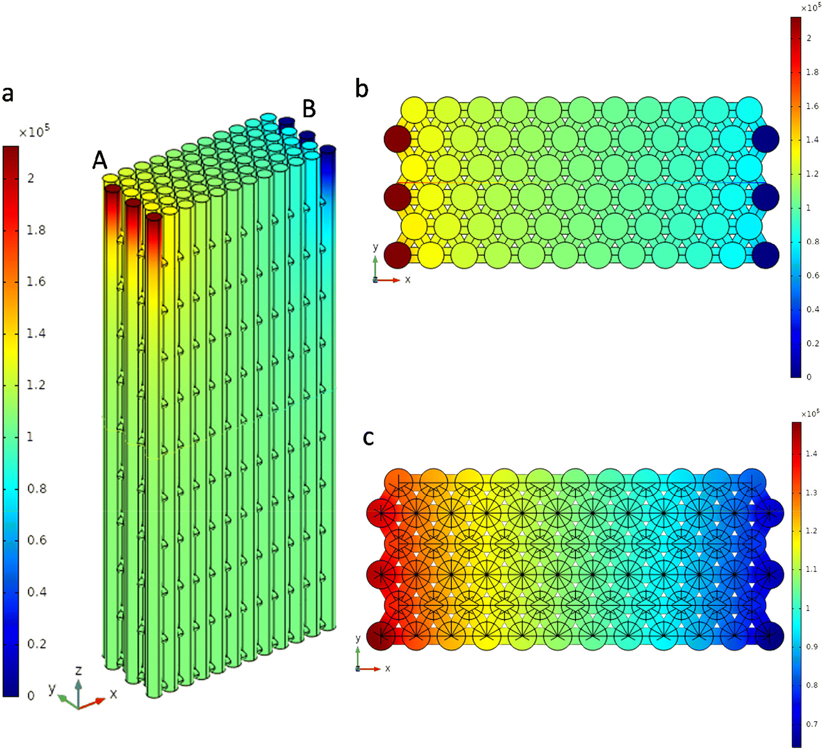 | ||
| Fig. 3 (a) Lateral perspective of the COMSOL geometry used in this simplified model of the measurement, once the simulation of the electrical conduction has been carried out, where the two terminals can be seen (A being the input terminal and B the ground), (b) top view of the COMSOL simulation of the electrical conduction, and (c) sectional view of the first plane of transversal channels, where the main voltage drop along the structure takes place. | ||
The in-plane Seebeck coefficient was found to be −58.3 ± 6.0 μV K−1 at room temperature for the Cu0.61Ni0.39 film and −59.9 ± 6.0 μV K−1 for the 3D-Cu0.61Ni0.39 nanonetwork, indicating n-type conduction. This value is consistent with literature reports of −45 μV K−1 and −50 μV K−1 at room temperature for an electrodeposited Cu0.61Ni0.39 film on a silicon substrate3 and for a non-crystalline Cu0.55Ni0.45 bulk material,7 respectively. Then, the in-plane power factor (PF = σ·S2) was 4.4 ± 1.0 mW m−1 K−2 and 3.9 ± 0.9 mW m−1 K−2 at room temperature for the Cu0.61Ni0.39 film and for the 3D-Cu0.61Ni0.39 nanonetwork, respectively, which is slightly lower than that observed for the bulk material (5.5 mW m−1 K−2).7
The thermal conductivity, k, was determined by the photoacoustic method to obtain the thermal diffusivity, α, using the following equation:24
| k = α·ρ·Cp | (6) |
| Material | Porosity (%) | k comp (W m−1 K−1) | K CuNi (W m−1 K−1) |
|---|---|---|---|
| Cu0.61Ni0.39 film | — | — | 10.9 ± 1.1 |
| 1D-Cu0.59Ni0.41 nanowires | 49.5 ± 2.5 | 5.5 ± 0.5 | 10.0 ± 1.0 |
| Modulated-Cu0.59Ni0.41 nanowires | 49.6 ± 2.5 | 5.0 ± 0.5 | 9.1 ± 0.9 |
| 3D-Cu0.61Ni0.39 nanonetwork | 55.8 ± 2.8% | 5.3 ± 0.5 | 8.7 ± 0.9 |
However, to determine the thermal conductivity of the CuNi nanostructure without AAO, effective medium theory was applied, taking into account the density and specific heat of CuNi (ρ = 8934 kg m−3 and Cp = 418 J kg−1 K−1), the density and specific heat of the skeletal AAO template (ρ = 2800 kg m−3 and Cp = 780 J kg−1 K−1),27 and the porosity extracted from the SEM measurements of the different geometrical parameters of the templates and nanostructures.27,28
The out-of-plane thermal conductivities were found to be 10.9 ± 1.1, 10.0 ± 1.0, 9.1 ± 0.9 and 8.7 ± 0.9 W m−1 K−1 for the film, 1D-CuNi nanowires, modulated-CuNi nanowires, and 3D-CuNi nanonetworks without AAO, respectively. This trend indicates that the increasing surface-to-volume ratio of the different structures enhances phonon scattering and thus decreases the thermal conductivity. The film with the lowest surface-to-volume ratio has the highest thermal conductivity, even though it is nanostructured with grain sizes of around 20 nm (10.9 ± 1.1 W m−1 K−1). The 1D-nanowires show increased scattering (10.0 ± 1.0 W m−1 K−1), which is further enhanced in the modulated nanowires (9.1 ± 0.9 W m−1 K−1) due to their rough surface. The 3D-nanonetworks show the most significant reduction in thermal conductivity (k = 8.7 ± 0.9 W m−1 K−1), with the transverse channels acting as effective phonon scattering centers.
Since thermal conductivity is the combination of electronic thermal conductivity (ke) and lattice thermal conductivity (kl), to distinguish between the contribution of phonons and electrons to the thermal conductivity, the Wiedemann–Franz law (ke = σ·L·T) has been used. In this equation, L is the Lorenz number (2.44 × 10⁻⁸ W Ω K−2),29σ is the measured electrical conductivity, and T is the temperature (298.15 K) (see Table 3).
| Material | k ⊥ (W m−1 K−1) | k e (W m−1 K−1) | k l (W m−1 K−1) |
|---|---|---|---|
| Cu0.61Ni0.39 film | 10.9 ± 1.1 | 9.5 ± 0.5 | 1.4 ± 0.3 |
| 3D-Cu0.61Ni0.39 nanonetwork | 8.7 ± 0.9 | 8.1 ± 0.4 | 0.6 ± 0.2 |
| Cu0.55Ni0.45 bulk7 | 29 | 15.4 | 13.6 |
Table 3 shows that the contribution of electrons to the electronic thermal conductivity (ke) is approximately 87.2 and 93.1% of the total thermal conductivity for the Cu0.61Ni0.39 film and 3D-Cu0.61Ni0.39 nanonetwork, respectively, compared to ∼53% for the Cu0.55Ni0.45 bulk alloy.7 In fact, the lattice thermal conductivity (kl) is reduced from 13.6 W m−1 K−1 for the bulk material to 1.4 ± 0.3 W m−1 K−1 due to the crystallite size reduction and even further to 0.6 ± 0.2 W m−1 K−1 due to the combination of the reduction of the crystal size, the phonon scattering at the nanowire surfaces and the further scattering in the transverse nanochannels, resulting in kl values approaching zero. Thus, we have achieved a maximum reduction in lattice thermal conductivity and consequently total thermal conductivity, due to the combination of reduced crystallite size and the unique structure of the 3D-CuNi nanonetwork.
The comparison of 3D-networks of three different materials such as 3D-CuNi interconnected nanonetworks in this work with 3D-Bi2Te3 interconnected nanonetworks23 and 3D-PEDOT interconnected polymer nanonetworks30 reveals a significant reduction in the kl of the 3D-nanonetworks of the inorganic materials compared to their bulk counterparts. The 3D-CuNi nanonetworks exhibit a remarkable reduction in thermal conductivity due to phonon scattering at the intricate interfaces of the 3D-network architecture, achieving kl values close to zero, which is crucial for thermoelectric efficiency. This strong reduction in kl was also observed in 3D-Bi2Te3 networks, although the crystallite size in the Bi2Te3 network was larger than that in this study. Thus, it is clear that the 3D-nanonetwork plays a crucial role in the phonon transport mechanism for these two inorganic materials. This behavior does not seem to be the case for polymers, given that for the 3D-PEDOT nanonetwork, no improvement in the thermoelectric properties was observed. The electrical conductivity of the 3D-networks is similar to that of the electrodeposited films in all the cases. However, an increase in the Seebeck coefficient seems to occur in the 3D-nanonetworks of Bi2Te3, while this is not the case in the 3D-CuNi nanonetworks or in the polymeric 3D-PEDOT nanonetwork. Taken together, these studies underscore the importance of material composition and structural design in tailoring thermoelectric properties, highlighting the potential of nanostructured materials to outperform their bulk counterparts and contribute to sustainable energy solutions.
Considering the material as isotropic, the thermoelectric figure of merit, zT*, (zT = (σ·S2/k)·T) at room temperature (298.15 K) was found to be 0.12 ± 0.03, 0.22 ± 0.05, and 0.24 ± 0.06, respectively, for the Cu0.61Ni0.39 film, the 3D-Cu0.61Ni0.39 nanonetwork within the AAO template, and the free-standing 3D-Cu0.61Ni0.39 nanonetwork (see Table 4). For the free-standing 3D-CuNi nanonetwork, the AAO was removed and the thermal conductivity was calculated from the thermal conductivity of the CuNi and the thermal conductivity of air (2.6 × 10⁻² W m−1 K−1).31
| Material | σ ∥ (Ω m)−1 | S ∥ (μV K−1) | k ⊥ (W m−1 K−1) | zT* at RT |
|---|---|---|---|---|
| Cu0.61Ni0.39 film | 1.3 ± 0.1 | −58.3 ± 6.0 | 10.9 ± 1.1 | 0.12 ± 0.03 |
| 3D-Cu0.61Ni0.39 nanonetwork within the AAO template | 1.1 ± 0.1 | −59.9 ± 6.0 | 5.3 ± 0.5 | 0.22 ± 0.05 |
| Free-standing 3D-Cu0.61Ni0.39 nanonetwork | 1.1 ± 0.1 | −59.9 ± 6.0 | 4.9 ± 0.6 | 0.24 ± 0.06 |
| Cu0.55Ni0.45 bulk7 | 2.1 | −52 | 29 | 0.05 |
A large increase in the figure of merit of more than four times (4.8 and 4.4) is observed when free-standing 3D-CuNi nanonetworks and 3D-CuNi nanonetworks within AAO templates are compared to Cu0.55Ni0.45 bulk7 (zT = 0.5 × 10⁻²).7 An increase of more than twofold (2.4) is observed when CuNi films are compared to bulk. The amount of CuNi used in a thermoelectric device made of these nanocrystalline 3D-CuNi nanonetworks is much lower than that in a bulk material, which significantly reduces the price of a final device.
It is worth mentioning that both materials composing these 3D-CuNi nanonetworks, anodic aluminum oxide nanostructures (anodization of Al) and CuNi alloys exhibit long-term stability due to the fact that anodization of Al is a well-known process to prevent oxidation of the Al component in aeronautics, the automotive industry, and building surfaces such as windows, roofed verandas, or terraces, and CuNi alloys are commonly used in the microelectronics industry due to their chemical and thermal stability over time. Moreover, 3D-CuNi nanonetworks are highly scalable for industrial applications as anodization and electrodeposition processes are well-established industrial processes, even for large surfaces.
4. Conclusions
In conclusion, this research successfully demonstrates the enhancement of the thermoelectric properties of CuNi alloys by electrodeposition, combining two nanostructuring techniques. On the one hand, the incorporation of saccharine into the electrolyte reduces the crystallite size to ∼25 nm. On the other hand, the use of three-dimensional anodic aluminum oxide (3D-AAO) templates enables the formation of 3D-nanonetworks. The values of these 3D-networks have been compared with those of nanocrystalline CuNi films, 1D-nanowire arrays, and 1D-modulated nanowire arrays. The consistent composition of Cu0.60Ni0.40 is the same for all the growth samples and with comparable crystallite size results in similar values of electrical conductivity and Seebeck coefficients. However, the thermal conductivity is the only parameter that changes due to the nanostructuration.The remarkable reduction in thermal conductivity, nearly halving from 29 W m−1 K−1 for bulk CuNi to 10.9 ± 1.1 W m−1 K−1 for nanocrystalline films, to even lower values such as 5.3 ± 0.5 W m−1 K−1 for the composite 3D-nanonetworks/alumina and 4.9 ± 0.6 W m−1 K−1 for free-standing 3D-nanonetworks, is attributed to enhanced phonon scattering due to increased surface area and reduced dimensionality. The calculated zT* (considering the material as isotropic) at room temperature was found to increase from the reported 0.05 value of the bulk material to 0.12 ± 0.03, 0.22 ± 0.05, and 0.24 ± 0.06 for the Cu0.61Ni0.39 film, the 3D-Cu0.61Ni0.39 nanonetwork within the AAO template, and the free-standing 3D-Cu0.61Ni0.39 nanonetwork, respectively. Therefore, an approximate (∼) five times increase in the figure of merit is observed when free-standing 3D-CuNi nanonetworks are compared to the bulk material. The high figure of merit (zT) values at room temperature for the free-standing CuNi alloy highlight the potential of these materials for application in thermoelectric generators, particularly in wearable technology and small-scale energy harvesting devices. This study not only reinforces the viability of CuNi alloys as competitive thermoelectric materials, but also sets the stage for future research aimed at optimizing their integration into practical energy conversion systems with environmentally friendly, long-term stable, scalable, and Earth abundant materials.
Data availability
The data supporting this article can be obtained on request from the corresponding author.Conflicts of interest
The authors declare no competing financial interest.Acknowledgements
The authors would like to acknowledge financial support from MINECO under grant number PID2020-118430GB-100. C. V. M. acknowledges financial support from “Atracción de Talento Investigador” de la Comunidad de Madrid, contract 2019-T1/IND-13541. We acknowledge the service from the MiNa Laboratory at IMN and funding from CM (project SpaceTec, S2013/ICE2822), MINECO (project CSIC13-4E-1794), and EU (FEDER, FSE).References
- O. Caballero-Calero, J. R. Ares and M. Martín-González, Adv. Sustainable Syst., 2021, 5, 2100095 CrossRef CAS.
- D. Beretta, N. Neophytou, J. M. Hodges, M. G. Kanatzidis, D. Narducci, M. Martin-Gonzalez, M. Beekman, B. Balke, G. Cerretti, W. Tremel, A. Zevalkink, A. I. Hofmann, C. Müller, B. Dörling, M. Campoy-Quiles and M. Caironi, Mater. Sci. Eng., R, 2019, 138, 100501 Search PubMed.
- R. G. Delatorre, M. L. Sartorelli, A. Q. Schervenski, A. A. Pasa and S. Güths, J. Appl. Phys., 2003, 93, 6154–6158 CrossRef CAS.
- Y. Shimizu, M. Mizoshiri, M. Mikami, J. Sakurai and S. Hata, J. Phys.: Conf. Ser., 2018, 1052, 012032 CrossRef.
- A. Sugihara, M. Kodzuka, K. Yakushiji, H. Kubota, S. Yuasa, A. Yamamoto, K. Ando, K. Takanashi, T. Ohkubo, K. Hono and A. Fukushima, Appl. Phys. Express, 2010, 3, 065204 CrossRef.
- M. Wolf, J. Flormann, T. Steinhoff, G. Gerstein, F. Nürnberger, H. J. Maier and A. Feldhoff, Alloys, 2022, 1, 3–14 CrossRef.
- H. Muta, K. Kurosaki, M. Uno and S. Yamanaka, J. Alloys Compd., 2003, 359, 326–329 CrossRef CAS.
- M. Yuan, L. Sun, X. W. Lu, P. Jiang and X. H. Bao, Mater. Today Phys., 2021, 16, 100311 Search PubMed.
- D. A. Borca-Tasciuc, G. Chen, A. Prieto, M. S. Martin-Gonzalez, A. Stacy, T. Sands, M. A. Ryan and J. P. Fleurial, Appl. Phys. Lett., 2004, 85, 6001–6003 CrossRef CAS.
- F. Domínguez-Adame, M. Martín-González, D. Sanchez and A. Cantarero, Phys. E, 2019, 113, 213–215 Search PubMed.
- C. V. Manzano, O. Caballero-Calero, M. Tranchant, E. Bertero, P. Cervino-Solana, M. Martin-Gonzalez and L. Philippe, J. Mater. Chem. C, 2021, 9, 3447–3454 RSC.
- E. Pellicer, A. Varea, S. Pané, B. J. Nelson, E. Menéndez, M. Estrader, S. Suriñach, M. D. Baró, J. Nogués and J. Sort, Adv. Funct. Mater., 2010, 20, 983–991 CrossRef CAS.
- E. Pellicer, A. Varea, S. Pané, K. M. Sivaraman, B. J. Nelson, S. Suriñach, M. D. Baró and J. Sort, Surf. Coat. Technol., 2011, 205, 5285–5293 CrossRef CAS.
- C. V. Manzano, P. Schürch, L. Pethö, G. Bürki, J. Michler and L. Philippe, J. Electrochem. Soc., 2019, 166(10), E1–E7 CrossRef.
- H. Masuda and K. Fukuda, Science, 1995, 268, 1466–1468 CrossRef CAS PubMed.
- C. V. Manzano, J. P. Best, J. J. Schwiedrzik, A. Cantarero, J. Michler and L. Philippe, J. Mater. Chem. C, 2016, 4, 7658–7666 RSC.
- J. Martín, M. Martín-González, J. Francisco Fernández and O. Caballero-Calero, Nat. Commun., 2014, 5, 5130 CrossRef PubMed.
- A. Ruiz-Clavijo, Y. Tsurimaki, O. Caballero-Calero, G. Ni, G. Chen, S. V. Boriskina and M. Martín-González, ACS Photonics, 2018, 5, 2120–2128 CrossRef CAS.
- C. V. Manzano, J. Rodríguez-Acevedo, O. Caballero-Calero and M. Martín-González, J. Mater. Chem. C, 2022, 10, 1787–1797 RSC.
- T. A. Green, A. E. Russell and S. Roy, J. Electrochem. Soc., 1998, 145, 875–881 CrossRef CAS.
- G. B. Harris, Philos. Mag., 1952, 43, 113–123 Search PubMed.
- B. Abad, M. Rull-Bravo, S. L. Hodson, X. Xu and M. Martin-Gonzalez, Electrochim. Acta, 2015, 169, 37–45 CrossRef CAS.
- A. Ruiz-Clavijo, O. Caballero-Calero, C. V. Manzano, X. Maeder, A. Beardo, X. Cartoixà, F. X. Álvarez and M. Martín-González, ACS Appl. Energy Mater., 2021, 4, 13556–13566 CrossRef CAS PubMed.
- D. R. Lide, CRC Handbook of Chemistry and Physics, 90th edn, 2009 Search PubMed.
- H. Hu, X. Wang and X. Xu, J. Appl. Phys., 1999, 86, 3953–3958 CrossRef CAS.
- C. V. Manzano, B. Abad, M. Muñoz Rojo, Y. R. Koh, S. L. Hodson, A. M. Lopez Martinez, X. Xu, A. Shakouri, T. D. Sands, T. Borca-Tasciuc and M. Martin-Gonzalez, Sci. Rep., 2016, 6, 19129 CrossRef CAS PubMed.
- B. Abad, J. Maiz and M. Martin-Gonzalez, J. Phys. Chem. C, 2016, 120, 5361–5370 CrossRef CAS.
- B. Abad, J. Maiz, A. Ruiz-Clavijo, O. Caballero-Calero and M. Martin-Gonzalez, Sci. Rep., 2016, 6, 38595 CrossRef CAS PubMed.
- H.-S. Kim, Z. M. Gibbs, Y. Tang, H. Wang and G. J. Snyder, APL Mater., 2015, 3, 041506 CrossRef.
- C. V. Manzano, O. Caballero-Calero, A. Serrano, P. M. Resende and M. Martín-González, Nanomaterials, 2022, 12(24), 4430 CrossRef CAS PubMed.
- B. Graczykowski, A. El Sachat, J. S. Reparaz, M. Sledzinska, M. R. Wagner, E. Chavez-Angel, Y. Wu, S. Volz, Y. Wu, F. Alzina and C. M. Sotomayor Torres, Nat. Commun., 2017, 8, 415 CrossRef CAS PubMed.
Footnote |
| † Electronic supplementary information (ESI) available. See DOI: https://doi.org/10.1039/d4nr05292g |
| This journal is © The Royal Society of Chemistry 2025 |