DOI:
10.1039/D4RA08468C
(Paper)
RSC Adv., 2025,
15, 1766-1775
Optimizing the properties of In–N dual-doped SnO2 films: incorporation of nitrogen into the SnO2 lattice at the optimal content via direct current sputtering
Received
1st December 2024
, Accepted 14th January 2025
First published on 20th January 2025
Abstract
Direct current magnetron sputtering was employed to fabricate In–N dual-doped SnO2 films, with varying concentrations of N2 in a mixed sputtering gas of N2 and argon (Ar). The quantity of N-substituted O elements in the SnO2 lattice was confirmed through energy-dispersive X-ray spectroscopy (EDX) and X-ray photoelectron spectroscopy (XPS). A comprehensive investigation of properties of the In–N dual-doped SnO2 films was conducted using various techniques, including X-ray diffraction analysis, field-emission scanning electron microscopy (FESEM), atomic force microscopy (AFM), ultraviolet absorption spectroscopy, Hall effect measurements, and current–voltage (I–V) characteristic assessments. The results indicated that when the ratio of N2 to the mixed gas (Ar + N2) exceeded 15%, the films exhibited p-type conductivity. The films demonstrated optimal electrical and structural properties at an N2 content of 45%, with a resistivity of 5.1 × 10⁻³ Ω cm, hole mobility of 12.75 cm2 V−1 s−1, crystal grain size of 25.74 nm, and a root mean square (RMS) roughness of 0.61 nm, resulting in the highest photocurrent at the INTO-45/Si interface.
1. Introduction
Semiconductor technology has consistently advanced to fulfill societal demands. Semiconductor chip technology has achieved unparalleled levels of downsizing. As the semiconductor industry progresses, continuous research on transparent conductive oxides (TCOs) continues in pursuit of additional advancements. TCOs, which include n- and p-type semiconductors, are utilized in opto-electronic devices such as solar cells,1–10 various LED types,11–16 transparent transistors,17–19 thermochromic windows,20–22 and electrochromic windows.23–25 Although n-type TCOs have demonstrated encouraging outcomes, ongoing research focuses on p-type TCOs to broaden their utilization in opto-electronic systems. As detailed in the literature, n-type TCOs as In2O3 doped with Sn (ITO), ZnO doped with group III metal elements, and SnO2 doped with F, Sb, or Ta not only have great optical transparency but also possess remarkable conductivity. This is due to the fact that nearly all defects in the host lattice act as donors without being accompanied by a charge compensation effect, along with the presence of native oxygen vacancies (VO). Conversely, p-type transparent conductive oxides (TCOs) such as ZnO or SnO2 have not been able to reach the requisite level of electrical conductivity. This is because there is a charge compensation interaction between substituted acceptors and native donors such as VO or interstitial dopants. The introduction of group I metals, including Na,26,27 Ag,28 and Li,29 or group V elements such as N,30 P,31 and As32 into ZnO results in a low density of holes. This arises from the limited solubility of the doped elements within the ZnO lattice and the charge compensation effect between doped acceptors and VO. In addition, the incorporation of doped group III elements, including Ga, In, Sc, B, and Al, into the ZnO lattice facilitates n-type conduction. In contrast, a more varied range of metallic elements, specifically from groups I, II, and III, into SnO2 for doping, rather than using ZnO, has the potential to produce a p-type semiconductor with greater hole concentration. Nevertheless, as previously mentioned, the issue of charge compensation between substituted acceptors and inherent VO defects persists within the host lattice when SnO2 doping single metal such as Ga, Zn and In.33–35 In order to eliminate or reduce the effects of charge compensation, an investigation of N incorporation into the SnO2 lattice at VO sites was conducted. Recent research has suggested that simultaneous doping with dual dopants such as Al–N, Ga–N, Zn–N, and Sb–N,36–43 can help decrease charge compensation or release holes from substituted acceptors in SnO2. In fact, studies have revealed that single metal doping (Ga, Zn, or In) in SnO2 results in a low hole concentration of around 1018 cm−3,33–35 but dual metal-N doping in SnO2 achieves a concentration of 1020 cm−3, signifying an enhancement of two orders of magnitude.36,38,41–43 A dual In–N dopant could be a viable alternative to dual mentioned dopants, as long as the charge compensation effect is kept to a minimum. Nonetheless, the current research does not address the role of lowering charge compensation in In–N dual doped SnO2 films. To address these challenges, this work describes generating In–N dual doped SnO2 films with varying N concentrations in a mixed sputtering environment using direct current magnetron sputtering.
2. Materials and methods
2.1. Deposition of In–N dual doped SnO2 films
In this study, In–N dual doped SnO2 (INTO-x) films were grown on quartz and Si substrates employing a direct current sputtering technique in a mix of Ar and x% N2 (x = 0, 15, 30, 45, and 60) gas at a working pressure of 10−3 torr. Substrates were heated at 300 °C before depositing films. The production of the In2O3-doped SnO2 (INTO) ceramic target consisted of combining 95 wt% SnO2 Merck powder with a purity of 99.999% and 5 wt% In2O3 Merck powder with a purity of 99.999%. This mixture was then subjected to grinding, drying, and hydraulic pressing to form a circular disc with a radius of 1.5 inches. Finally, the disc underwent six hours of sintered operation at 1500 °C. The German-made Leybold Univex 450 vacuum chamber was evacuated to 10−6 torr of pressure prior to the thin-film fabrication process. A high-purity mixed gas, with each gas type having a purity level of 99.9999%, was delivered into the vacuum system via two flowmeters adjusted to the appropriate rate. The INTO-x films were produced with a power of 80 W and a substrate-target distance of 8 cm. The cleaning process for the quartz substrates included the utilization of deionized water, acetone, and sodium hydroxide. On the other hand, the Si substrates were cleaned using trichloroethylene, isopropanol, diluted hydrofluoric acid, deionized water, and acetone. The substrates were desiccated using a stream of pure N2 gas. The experiment utilized n-type Si (100) substrates possessing the resistivity ranging from 1 to 10 Ω cm and the carrier concentration of 1 × 1016 cm−3.
2.2. Techniques for characterization
The transparency of the INTO-x/quartz films was assessed by analyzing the transmittance spectra in the wavelength range of 190–1100 nm using a V-630 system manufactured by JASCO in Japan. Electrical characteristics were determined at a temperature of 30 °C by measuring Hall equipped with an HL5500PC system manufactured by Nanometrics Incorporated, USA. The elemental compositions of the films were analyzed utilizing microscopy, which is enhanced by electron scanning accompanied by field emission (EDX) with the JSM-IT800 instrument manufactured by JEOL in Japan. The films' atomic compositions were examined using X-ray photoelectron spectroscopy (XPS) spectra, specifically the AXIS Ultra DLD instrument by KRATOS-SHIMADZU in Japan. X-ray diffraction (XRD) studies were conducted to verify the structural parameters of the INTO films, such as the dimensions of the crystal grains, the nature of the lattice planes, and any alterations in the diffraction angles. The analysis utilized a Shimadzu 6100 diffractometer, made by SHIMADZU CORPORATION in Japan, which was outfitted with a copper-Kα radiation source and the 2θ scan step of 0.01° is set up. Morphological examinations were performed utilizing microscopy, which is enhanced by electron scanning accompanied by field emission (FESEM, JSM-IT800). The smoothness of the surface was evaluated using microscopy based on atomic force interaction (AFM) with a Bruker Dimension Edge system. The conversion of photon energy to electrical energy was assessed by analyzing the current–voltage graphs derived from experiments conducted under both light and non-illuminated conditions. The measurements were performed using a Keithley source, namely the model 2450, in conjunction with a simulated AM 1.5 solar source.
3. Analysis results and discussion
3.1. Elemental composition of INTO-x films via EDX analysis
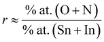
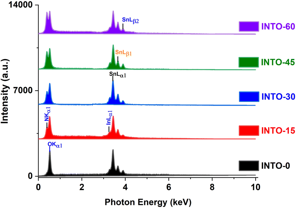
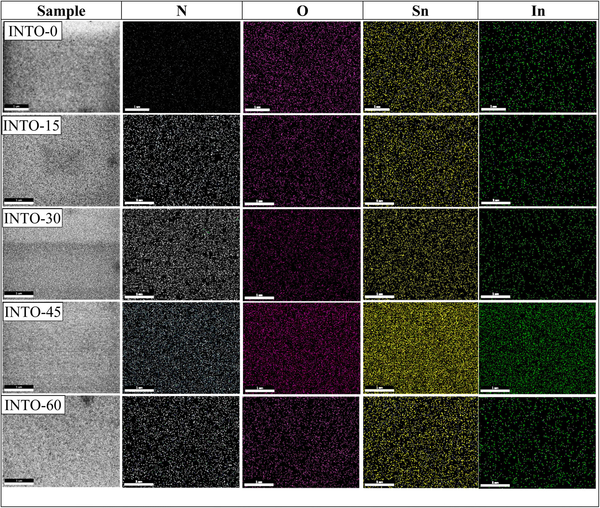
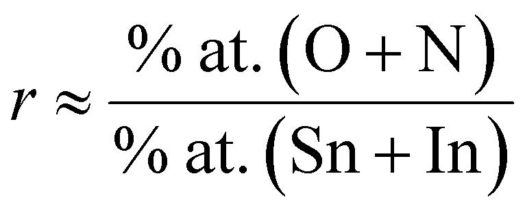
To accurately ascertain the oxygen concentration in INTO films via EDX analysis, the films were deposited on Si wafer. The EDX spectra of the INTO-x films in Fig. 1 shows binding energy peaks locating at 0.39 and 0.52 keV, attributed to N and O Kα1 characteristic peaks, respectively, whereas a peak at around 3.29 keV corresponds to the Lα1 distinctive binding energy of Indium. Additionally, the binding energy peaks were seen at 3.44, 3.66, and 3.9 keV, corresponding to the distinctive peaks of Sn including Lα1, Lβ1, and Lβ2. Fig. 2 presents a colour map of all elements, illustrating a uniform elemental distribution over the entire sample. The atomic composition results of the INTO-x films, deposited according to the experimental settings outlined in Section 2, are presented in Table 1, demonstrating fluctuations in N and O atomic concentrations relative to x whereas the Sn and In concentrations remained nearly constant. This indicates that the presence of N-substituted O in the SnO2 lattice. Furthermore, the r ratio, defined as the ratio of total of (O + N) to that of (Sn + In) content, was low for x = 0 and 15, but it approached 2 (1.91–1.94) when x exceeded than 15, thus aligning closely with the stoichiometry of SnO2. This signifies that O was substituted by N. The r ratio increased with x, indicating oxygen vacancies (VO) within the SnO2 lattice decreases as x rises. To further exactly determine the atomic content of INTO-x, X-ray photoelectron spectroscopy is employed to complement the EDX study.
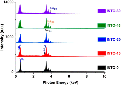 |
| | Fig. 1 EDX spectra of INTO-x films deposited on silicon substrates at 300 °C and 10−3 torr, with different percentages of N2 in a mixed sputtering gas. | |
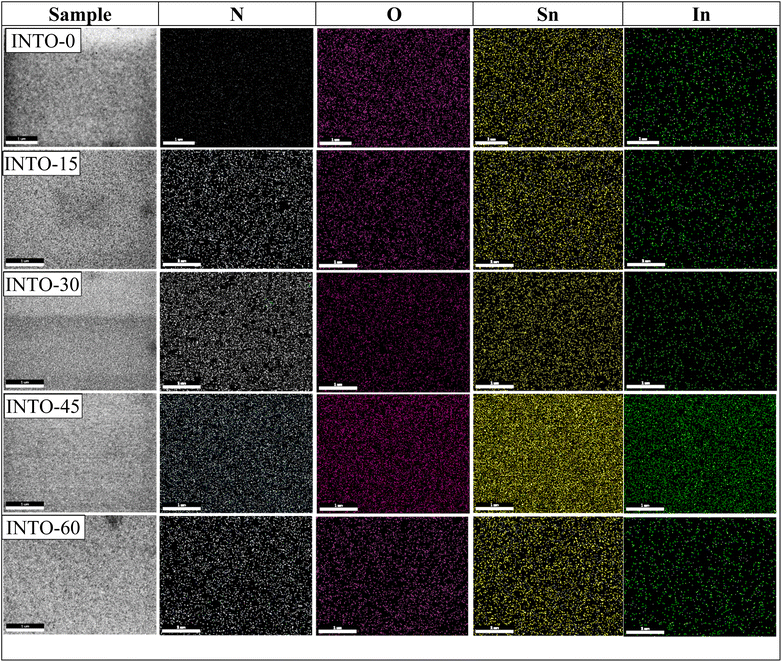 |
| | Fig. 2 EDX mapping images of INTO-x films deposited on quartz substrates at 300 °C and 10−3 torr, with different percentages of N2 in a mixed sputtering gas. | |
Table 1 Atomic composition of INTO-x samples with differing percentages of N2 in a mixed sputtering gas, as determined from EDX analysis
| Sample |
% at. N |
% at. O |
% at. Sn |
% at. In |
|
| INTO-0 |
1.04 |
61.81 |
32.5 |
4.65 |
1.69 |
| INTO-15 |
10.46 |
54.61 |
30.31 |
4.62 |
1.86 |
| INTO-30 |
14.62 |
51.06 |
29.64 |
4.68 |
1.91 |
| INTO-45 |
17.68 |
48.23 |
29.41 |
4.68 |
1.93 |
| INTO-60 |
18.74 |
47.28 |
29.36 |
4.62 |
1.94 |
3.2. Atomic composition of INTO-x films via XPS analysis
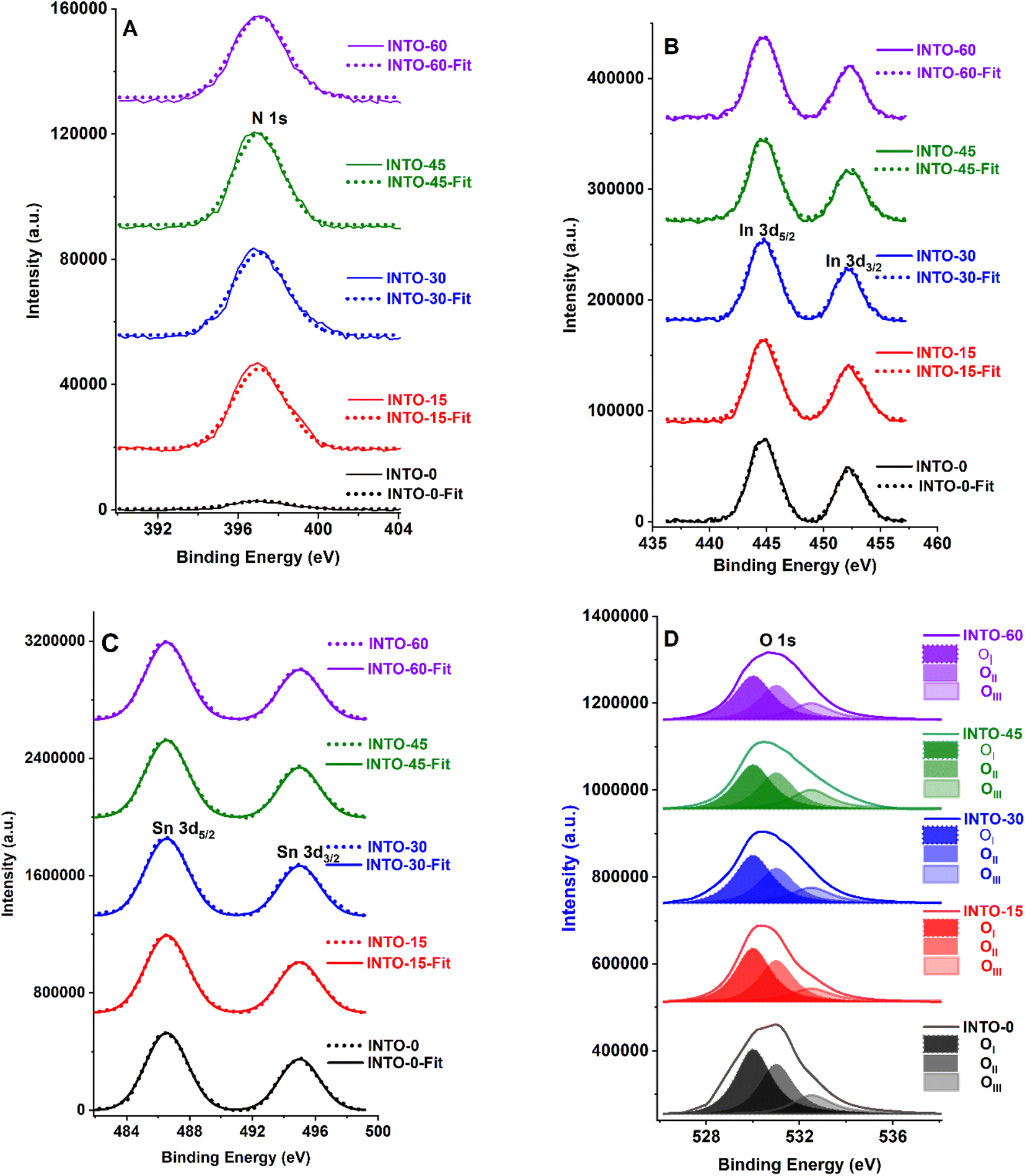
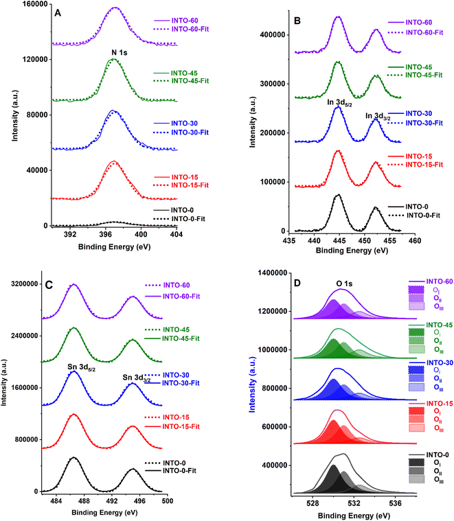
Fig. 3 displays the XPS core-level energy peaks of all elements of the INTO-x films, where x ranging from 0 to 60 in increments of 15. All XPS core-level energy peaks are calibrated based on C 1s binding energy peak at 284.5 eV. Fig. 3A indicates that the N 1s core-level energy is located at 396.9 eV, which is ascribed to the N-substituted O positions within the SnO2 crystal lattice. Fig. 3B presents the In 3d5/2 to 3d3/2 double core level energy peak, ranging from 444.7 to 452.3 eV, attributed to the substitution of Sn4+ by In3+. Also, Fig. 3C exhibits a Sn 3d5/2 to 3d3/2 double core-level peak located between 486.6 and 495 eV, attributed to the Sn–O bonding. Whereas Fig. 3D shows the O 1s binding energy peak at 530.5 eV, which was split into three sub-peaks: one at 530 eV, corresponding to the sufficient Sn–O bond, one at 531 eV, relating to the Sn–O bond influenced by VO, and another at 532.5 eV, associated with the surface absorbed O kinds. The atomic composition of INTO-x is given in Table 2, where the atomic percentage was determined using the formula, with i and j denoting In, N, O, or Sn. S and I denote atomic sensitivity parameters and the area of the core-level distinctive energy peaks.44 The results indicate that the r ratio escalates when x increases, particularly reaching 1.93–1.96 when x is between 30 and 60. The results vary slightly from those obtained through EDX analysis, as XPS can detect oxygen in regions with oxygen vacancies, whereas EDX fails to identify such locations of oxygen vacancies. These data further demonstrate that the lattice points of N-substituted O increases with x, indicating the XPS results are consistent with those of the EDX investigation, as detailed in Section 3.1. Thus, EDX and XPS investigations indicate that the presence of N-substituted O lattice points inside the host lattice escalated with x value, confirming the quantity of N-substituted O elements within the host lattice rises, as seen in Tables 1 and 2.
 |
| | Fig. 3 XPS spectra of INTO-x films deposited on quartz substrates at 300 °C and 10−3 torr, with different percentages of N2 in a mixed sputtering gas. | |
Table 2 Atomic composition of INTO-x samples with differing percentages of N2 in a mixed sputtering gas, as determined from XPS analysis
| Sample |
% at. N |
% at. O1 |
% at. O2 |
% at. O (% at. O1 + % at. O2) |
% at. Sn |
% at. In |

|
| INTO-0 |
1.21 |
35.66 |
26.45 |
62.11 |
32.16 |
4.52 |
1.73 |
| INTO-15 |
10.52 |
31.55 |
23.31 |
54.86 |
30.07 |
4.55 |
1.89 |
| INTO-30 |
14.71 |
29.36 |
21.81 |
51.17 |
29.59 |
4.53 |
1.93 |
| INTO-45 |
17.77 |
27.87 |
20.42 |
48.29 |
29.48 |
4.46 |
1.95 |
| INTO-60 |
18.97 |
27.16 |
20.11 |
47.27 |
29.25 |
4.51 |
1.96 |
3.3. Structural characteristics of INTO-x films via XRD patterns
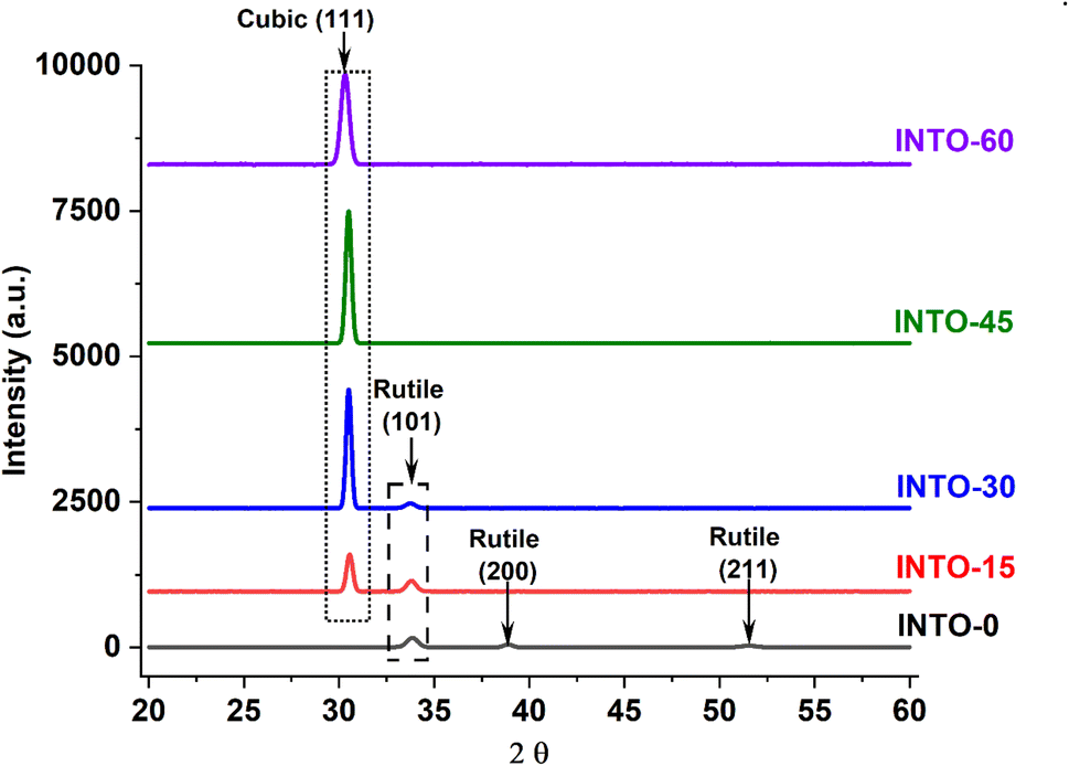
The crystal structure of undoped SnO2 films is typically tetragonal rutile, irrespective of the deposition process, and this rutile phase remains unchanged when SnO2 films are doped with metal elements such as Sb, In, Ga, and Zn, particularly when employing the dc magnetron technique.33–35 However, Al–N, Ga–N, Zn–N, and Sb–N -doped SnO2 films produced via dc magnetron technique showed a phase transition from rutile to cubic which is ascribed to the incorporation of N into SnO2 lattice.36,38,41–43 The crystal structure of In–N doped SnO2 showed the same phase transition as Al–N, Ga–N, Zn–N, and Sb–N -doped SnO2 films, as illustrated in Table 3 and Fig. 4. Fig. 4 shows In-doped SnO2 (INTO-0) possesses rutile phase characterized by three lattice reflections (101), (200) and (211), located at 2θ = 33.86, 38.88, and 51.53°, respectively. When In-doped SnO2 is deposited using a mixed sputtering gas containing 15% N2, a decline in the rutile reflection (101) is observed, alongside a total lack of rutile reflection (200), and the emergence of cubic reflection (111) at 2θ = 30.56°. This indicates the incorporation of N into the SnO2 lattice. A more distinct phase transition indicates greater degradation of the rutile reflection (101) and increased evolution of the cubic reflection (111). Consequently, the observation of solely the cubic reflection (111) along with a maximum crystal grain size of 25.74 nm suggests that the rutile-to-cubic phase transition is fully achieved at x = 45, which aligns with the deposition of INTO in a mixed sputtering gas comprising 45% N2. Table 3 indicates that optimal crystal quality is achieved with the maximum crystal grain size, as calculated using Scherer equation;27 nevertheless, crystal deterioration reoccurs when x exceeds 45, attributed to an excessive quantity of N-substituted O elements in the host lattice or the exceeding of the crystal structure's stability threshold. Table 3 additionally illustrates the N incorporation into the SnO2 lattice, as indicated by the 2θ shift of all reflections to the lower values with increasing x. Besides, the crystal grain size of cubic reflection (111) increases with x until x reaches 45, after which it falls when x exceeds 45, proving the substitution of O by N. This suggests that films with higher number of VO defects cause lattice distortion, thereby leading to poor crystal quality. Consequently, the incorporation of N into the SnO2 lattice corresponds to a reduction in the number of VO defects, leading to an increase in the crystal grain size of the cubic reflection (111) with increasing x. However, when x exceeds 45, crystal degradation occurs, resulting in a decrease in crystal grain size due to significant lattice broadening. Furthermore, lattice parameter of cubic reflection (111) increases with rising x, signifying that the quantity of N-substituted O elements rises with x.
Table 3 A structural data of INTO-x deposited on quartz substrates at 300 °C and 10−3 torr, with different percentages of N2 in a mixed sputtering gas calculated XRD patterns
| Sample |
Phase-(hkl) peak of SnO2 |
2θ (degree) |
Full-width at half-maximum (FWHM) (rad) |
Crystalline size D (nm) |
Average crystalline size D (nm) |
Lattice constant (Å) |
| INTO-0 |
Rutile (101) |
33.86 |
0.57 |
14.57 |
|
a200 (= b) 4.6312 |
| (200) |
38.88 |
0.51 |
16.53 |
13.40 |
|
| (211) |
51.53 |
0.81 |
10.89 |
|
c = 2.6377 |
| INTO-15 |
Rutile (101) |
33.81 |
0.59 |
14.08 |
17.88 |
a111 5.0652 |
| Cubic (111) |
30.56 |
0.38 |
21.68 |
|
|
| INTO-30 |
Rutile (101) |
33.75 |
0.62 |
13.40 |
18.14 |
a111 5.0700 |
| Cubic (111) |
30.53 |
0.36 |
22.89 |
|
|
| INTO-45 |
Cubic (111) |
30.50 |
0.32 |
25.74 |
25.74 |
a111 5.0749 |
| INTO-60 |
Cubic (111) |
30.32 |
0.51 |
16.15 |
16.15 |
a111 5.1043 |
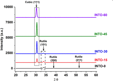 |
| | Fig. 4 XRD patterns of INTO-x films deposited on quartz substrates at 300 °C and 10−3 torr, with different percentages of N2 in a mixed sputtering gas. | |
3.4. Morphology of INTO-x films via FESEM
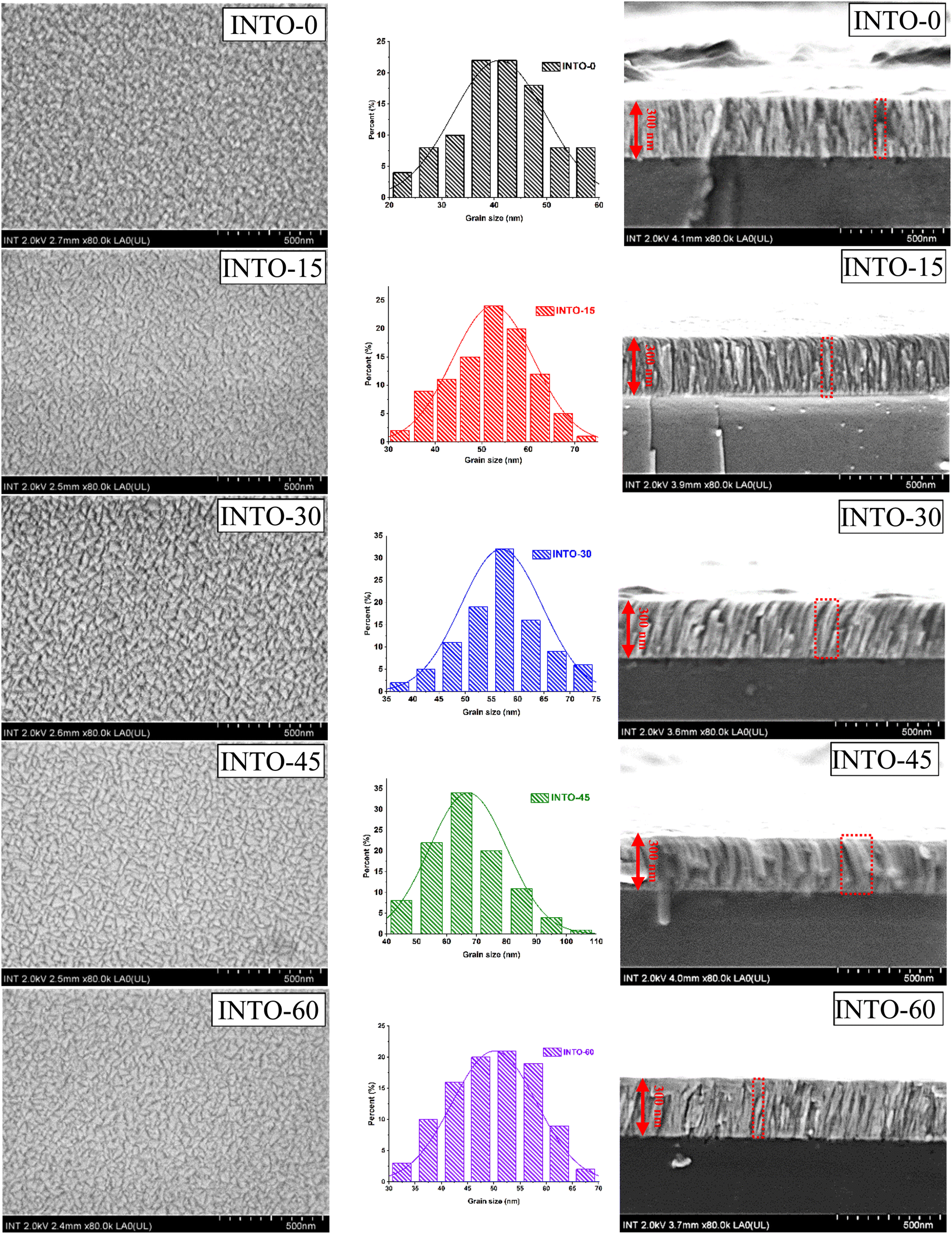
FESEM research complements XRD patterns for further investigation of the crystal structure influenced by the substitution of O with N in the SnO2 lattice. Fig. 5 displays FESEM images, encompassing surface and cross-sectional views, as well as the grain size distribution of INTO-x films. The results reveal that grain size grows with rising x until x equals 45; thereafter, it drops at x = 60, suggesting the presence of N-substituted O sites in the SnO2 lattice, which aligns with the study in Section 3.3. The top and side images from FESEM further illustrate that the replacement of O with N results in a denser structure, notably noticeable in the most compact structure of INTO-45. The maximum grain size of 68 nm for the INTO-45 film is demonstrated by the grain distribution, which further implies that the fluctuations in grain size match those seen in XRD analysis. Besides, cross-sectional images demonstrate that all of the films have a thickness of about 300 nm, exhibiting different widths throughout the samples as indicated in Fig. 5.
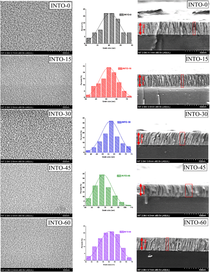 |
| | Fig. 5 FESEM images and grain size distribution spectra of INTO-x films deposited on quartz substrates at 300 °C and 10−3 torr, with different percentages of N2 in a mixed sputtering gas. | |
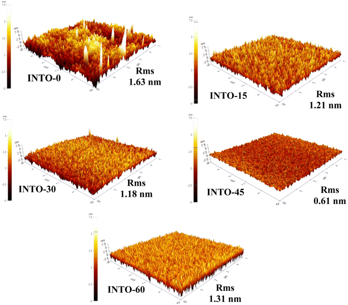
3.5. Morphology of INTO-x films via AFM
AFM images depict the surface morphology of films at the microscale, in of the surface smoothness of films diminishes progressively with increasing x until x reaches 45, which corresponds to the minimum surface smoothness or root mean square (RMS), attributed to the most quantity of N-substituted O spots within the host lattice. This demonstrated that the crystal quality improves, aligning with FESEM and XRD investigations. The dense surface of the FESEM image signifies a reduction in grain boundaries, leading to a decrease in the RMS of the AFM images. However, when films are deposited at x value over the threshold value of 45, the surface compactness observed in FESEM decreases which is the sequence of reducing N-substituted O points in the SnO2 lattice, which subsequently leads to an increase in RMS values in AFM images thereafter. In addition, Table 4 illustrates the correlation among average crystalline size, root mean square, and band gap of INTO-x samples in relation to varying amounts of different N2 in a mixed sputtering gas. The findings suggest that the number of VO defects diminishes with an escalation in N–VO substitution within the SnO2 lattice, resulting in an enhancement in film density. Notably, the highest film density or the largest average crystal size was associated with an optimal quantity of N-substituted O sites in the SnO2 lattice when x = 45, which is consistent with the literature.41,42 Furthermore, the band gap of INTO-x decreases with x, which is due to an increase in N-substituted O sites in the SnO2 lattice as explained in the next section (Fig. 6).
Table 4 Average crystalline size, root mean square and bandgap of INTO-x samples with different percentages of N2 in a mixed sputtering gas
| Sample |
% at. N |
Average crystalline size D (nm) |
RMS (nm) |
Bandgap (eV) |
| INTO-0 |
1.21 |
13.40 |
1.63 |
4.18 |
| INTO-15 |
10.52 |
17.88 |
1.21 |
3.96 |
| INTO-30 |
14.71 |
18.11 |
1.18 |
3.79 |
| INTO-45 |
17.77 |
25.74 |
0.61 |
3.73 |
| INTO-60 |
18.97 |
16.15 |
1.31 |
3.45 |
 |
| | Fig. 6 AFM images of INTO-x films deposited on quartz substrates at 300 °C and 10−3 torr, with different percentages of N2 in a mixed sputtering gas. | |
3.6. Optical transmittance spectra of INTO-x films
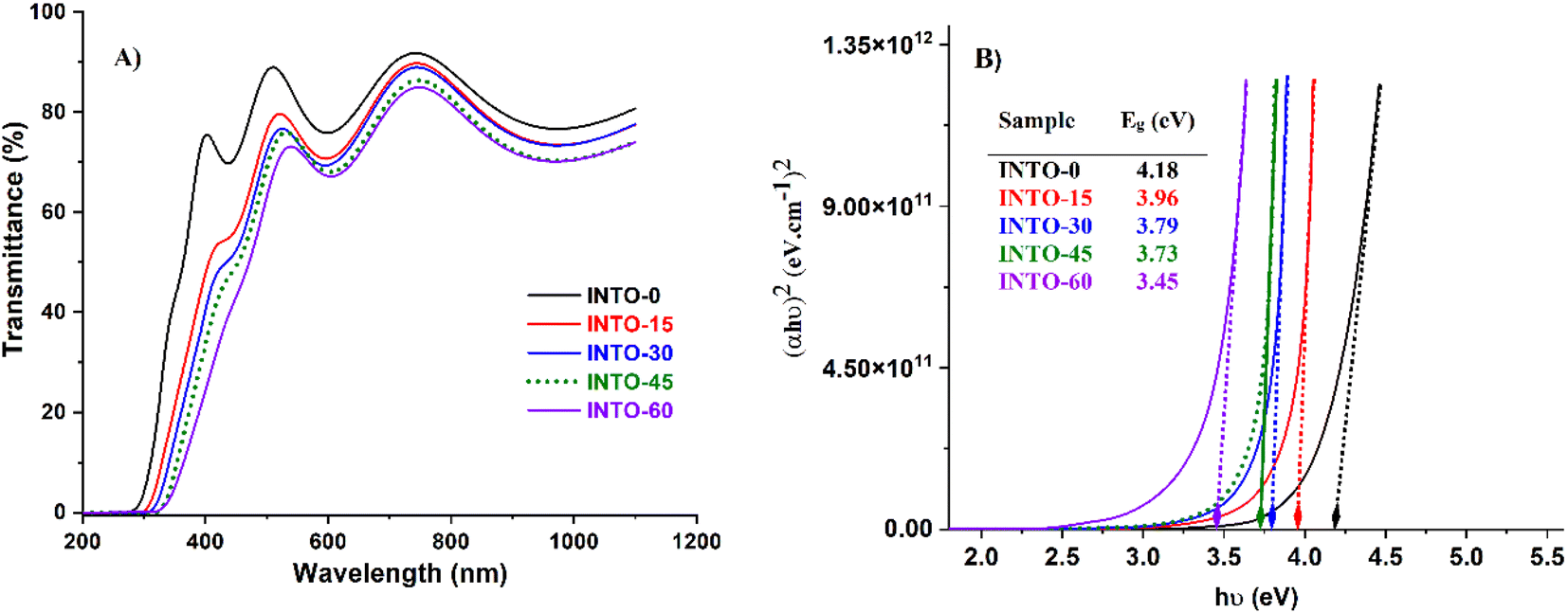
The optical transmittance spectra of INTO-x films were measured within the region of 200–1100 nm, as illustrated in Fig. 7A. The results indicate that the red shift of absorption edge occurs when x increases, attributed to the incorporation of N into the SnO2 lattice as discussed in the literature.36,38,41–43 The red shift of absorption edge indicates a reduction in bandgap energy, as illustrated in Fig. 7B. This is determined based on Tauc equation, where the (αhν)2 is a function of hν and the absorption coefficient (α) is a function varies with wavelength, as inferred from simulations performed with the Scout software. The findings show that the bandgap energy diminishes with the augmentation of N-substituted O elements in the SnO2 lattice, as ascertained through the EDX and XPS investigations in Sections 3.1 and 3.2.
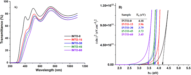 |
| | Fig. 7 Transmittance spectra (A) and bandgap energy (B) of INTO-x films deposited on quartz substrates at 300 °C and 10−3 torr, with different percentages of N2 in a mixed sputtering gas. | |
3.7. Electrical characteristics of INTO-x films
Despite containing approximately 4.5 at% In3+, INTO-0 functions as an n-type semiconductor, signifying that the VO donors prevail over the acceptors In3+. Therefore, N is doped into SnO2 to create p-type conductive SnO2 due to the integration of N3− acceptors into the host lattice. Table 5 demonstrates that the hole concentration of INTO films escalates with increasing x, signifying that N incorporation into the SnO2 lattice functions as acceptors, which aligns with the absorption edge of the transmittance spectra reported in Section 3.6. The results demonstrate that hole mobility increases with x, attributed to a decrease in VO in SnO2 and an improvement in crystal quality. The substitution of VO sites with N in the SnO2 lattice diminishes the attractive interaction between charge carriers and VO defects, as well as minimizes charge carrier scattering caused by VO defects. Furthermore, improved crystal quality diminishes charge carrier scattering at grain boundaries, aligning with literature reports.41,42 The INTO-45 film shows the lowest resistivity of 5.1 × 10⁻³ Ω cm and the highest hole mobility of 12.75 cm2 V−1 s−1. In contrast, the resistivity of the INTO-60 film rises while hole mobility decreases, which is indicative of crystal degradation, aligning with the XRD results presented in Section 3.3.
Table 5 Resistivity, carrier concentration and carrier mobility of INTO-x films deposited on quartz substrates at 300 °C and 10−3 torr, with differing percentages of N2 in a mixed sputtering gas
| Samples |
Resistivity ρ (Ω cm) |
Mobility μ (cm2 V−1 s−1) |
Carrier concentration n (cm−3) |
Type |
| INTO-0 |
4.5× 100 |
1.24 |
−1.12 × 10¹⁸ |
n |
| INTO-15 |
7.5 × 10⁻² |
2.58 |
3.23 × 10¹⁹ |
p |
| INTO-30 |
1.5 × 10⁻² |
5.13 |
8.12 × 10¹⁹ |
p |
| INTO-45 |
5.1 × 10⁻³ |
12.75 |
9.61 × 10¹⁹ |
p |
| INTO-60 |
9.0 × 10⁻³ |
6.43 |
1.05 × 10²⁰ |
p |
3.8. Testing photo-electrical effect of INTO-x/Si
All of INTO-x (where x ranges from 15 to 60) is deposited on Si substrates to examine the photo-electronic effects of the p–n junction, with the I–V measurement conditions detailed in Section 2.2. The current (I) – voltage (V) characteristics of In/INTO-x and In/Si interfaces exhibit linear behavior, indicating ohmic contact, and are not illustrated here. Fig. 8A illustrates a schematic structural model for assessing the photoelectronic effect at the INTO/Si interface. Fig. 8B illustrates the dark I–V characteristics of In/INTO-x/Si/In, exhibiting non-linear or rectified behavior, hence indicating that INTO-x functions as a p-type semiconductor. The findings indicate that the dark reverse bias current of In/INTO-45/Si/In is optimized owing to enhanced crystal quality, reduced RMS value, and minimal resistivity. Under illumination, the reverse bias current of all INTO-x/Si interfaces substantially increases compared to the dark reverse bias current, as the generated internal electric field accelerates photocarriers toward the two indium electrodes. The photocurrent at the INTO-45/Si interface under reverse bias is maximal, signifying that INTO-45 exhibits the most advantageous electrical and structural characteristics. The photocurrent value is proportional to with the crystal quality and electrical characteristics of the films.
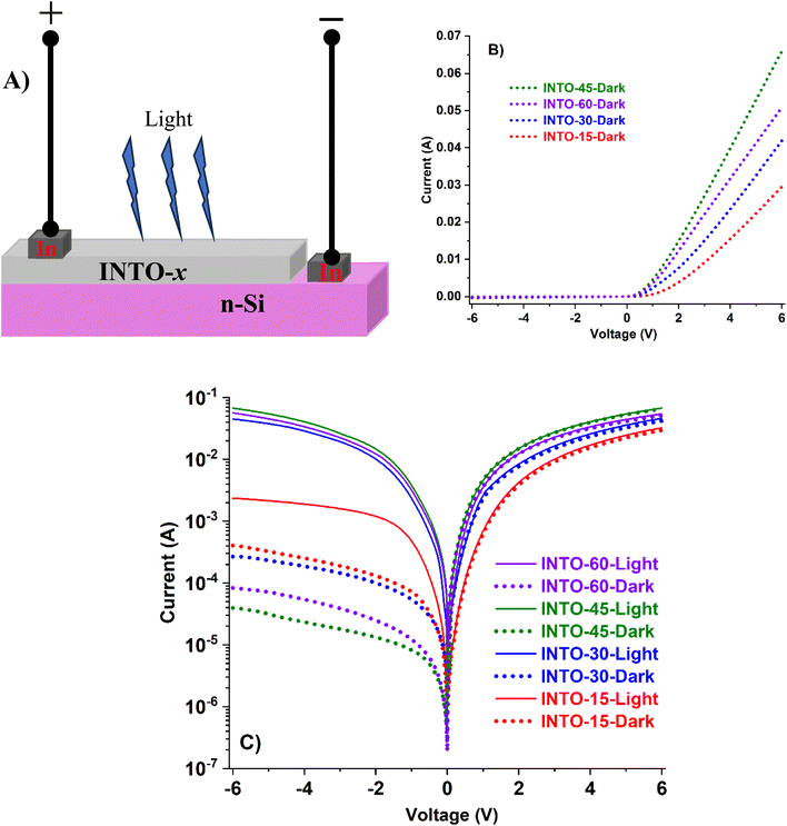 |
| | Fig. 8 I–V characteristics of INTO-x films deposited on Si substrates at 300 °C and 10−3 torr, with different percentages of N2 in a mixed sputtering gas. | |
4. Conclusion
Investigations using EDX and XPS verified that N3− had replaced O2−. The redshift of the absorption edge in transmittance spectra, an increase in hole concentration, an improvement in crystal quality, and an increase in reverse photocurrent of INTO/Si interfaces all indicate that the amount of N-substituted O elements in SnO2 increases with the N2 content in mixed sputtering gas. The ideal characteristics of the INTO-45 film, which is deposited in 45% N2 of the mixed sputtering gas, include the maximum hole mobility of 12.75 cm2 V−1 s−1 which is surpassed only by that of SnO2 doped with Zn–N (15.6 cm2 V−1 s−1), the lowest roughness of 0.61 nm – lower than that of SnO2 doped with Zn–N, Sb–N, Al–N, and Ga–N, the lowest resistivity of 5.1 × 10⁻³ Ω cm which is exceeded solely by SnO2 doped with Zn–N (3.8 × 10⁻³ Ω cm), and the highest crystal grain size of 25.74 nm. The outcomes provide maximal photocurrent for INTO-45/Si interface.
Data availability
All data relevant for the reproduction of the results presented in this work are included within the article.
Conflicts of interest
There are no conflicts to declare.
Acknowledgements
This research is funded by University of Science, VNU-HCM under grant number T2024-09.
References
- V. Sittinger, H. King, A. Kaiser, S. Jung, Ö. Ş. Kabakli, P. S. C. Schulze and J. C. Goldschmidt, Surf. Coat. Technol., 2023, 457, 129286 CrossRef CAS.
- T. Hölscher, M. Placidi, I. Becerril-Romero, R. Fonoll-Rubio, V. Izquierdo-Roca, A. Thomere, E. Bailo, T. Schneider, H. Kempa, R. Scheer and A. Pérez-Rodríguez, Sol. Energy Mater. Sol. Cells, 2023, 251, 112169 CrossRef.
- N. Ohashi, R. Kaneko, C. Sakai, Y. Wasai, S. Higuchi, K. Yazawa, H. Tahara, T. Handa, T. Nakamura, R. Murdey, Y. Kanemitsu and A. Wakamiya, Sol. RRL, 2023, 7, 2300221 CrossRef CAS.
- I. - Haq, M. I. Khan, M. Irfan, M. Fatima, H. H. Somaily, Z. M. Elqahtani and N. Alwadai, Ceram. Interfaces, 2023, 49, 29622–29629 CrossRef CAS.
- S. K. Swami, J. I. Khan, V. Dutta, J. Lee, F. Laquai and N. Chaturvedi, ACS Appl. Energy Mater., 2023, 6, 2906–2913 CrossRef CAS.
- H. W. Lee, S. Biswas, H. Choi, Y. Lee and H. Kim, Appl. Surf. Sci., 2024, 659, 159930 CrossRef CAS.
- Z. Yan, J. Shi, S. Chen, J. Du, L. Zhang, Q. Yuan, C. Song, K. Jiang, Y. Yang, A. Han, Z. Liu and F. Meng, Sol. Energy Mater. Sol. Cells, 2023, 253, 112244 CrossRef CAS.
- F. Ceh-Cih, E. Camacho-Espinosa, I. Rimmaudo, R. Mis-Fernández, S. Uc-Canché and J. L. Peña, Sol. Energy, 2024, 273, 112549 CrossRef CAS.
- R. Ramarajan, N. Purushothamreddy, R. K. Dileep, M. Kovendhan, G. Veerappan, K. Thangaraju and D. Paul Joseph, Sol. Energy, 2020, 211, 547–559 CrossRef CAS.
- J. Zhou, X. Zhang, H. Chen, Z. Tang, D. Meng, K. Chi, Y. Cai, G. Song, Y. Cao and Z. Hu, Appl. Surf. Sci., 2020, 534, 147632 CrossRef CAS.
- N. Gagrani, K. Vora, S. Adhikari, Y. Jiang, C. Jagadish and H. H. Tan, Adv. Opt. Mater., 2022, 10, 2102690 CrossRef CAS.
- S. González, G. Vescio, J. L. Frieiro, A. Hauser, F. Linardi, J. López-Vidrier, M. Oszajca, S. Hernández, A. Cirera and B. Garrido, Adv. Mater. Interfaces, 2023, 10, 2300035 CrossRef.
- J. Jing, L. Lin, K. Yang, H. Hu, T. Guo and F. Li, Org. Electron., 2022, 103, 106466 CrossRef CAS.
- M. N. Rezaie, S. Mohammadnejad and S. Ahadzadeh, Opt. Laser Technol., 2021, 138, 106896 CrossRef CAS.
- Y. J. Kim, B. W. Kim and S. H. Im, Adv. Mater. Interfaces, 2024, 11, 2400020 CrossRef CAS.
- S. Sreekumar, V. Bruevich, V. Podzorov and D. M. O'Carroll, Appl. Surf. Sci., 2024, 670, 160596 CrossRef CAS.
- B. S. Sannakashappanavar, A. B. Yadav, K. Singh and T. A. Sai, Micro and Nanostructures, 2023, 179, 207581 CrossRef CAS.
- R. A. Rodriguez-Davila, R. A. Chapman, Z. H. Shamsi, S. J. Castillo, C. D. Young and M. A. Quevedo-Lopez, Microelectron. Eng., 2023, 279, 112063 CrossRef CAS.
- C. Avis, M. M. Billah and J. Jang, Adv. Photonics Res., 2024, 5, 2300215 CrossRef CAS.
- W. Jin, K. Park, J. Y. Cho, S.-H. Bae, M. Siyar, H. Jang and C. Park, Ceram. Interfaces, 2023, 49, 10437–10444 CrossRef CAS.
- Z. Fang, S. Tian, B. Li, Q. Liu, B. Liu, X. Zhao and G. Sankar, Appl. Surf. Sci., 2021, 540, 148414 CrossRef CAS.
- H. Liu, H. Zong, L. Yan, D. Zhou, Y. Yin, G. Cao, L. Bian, C. Kang and M. Li, Infrared Phys. Technol., 2021, 113, 103648 CrossRef CAS.
- S. J. Lee, S. H. Lee, H. W. Kang, S. Nahm, B. H. Kim, H. Kim and S. H. Han, Chem. Eng. J., 2021, 416, 129028 CrossRef CAS.
- A. Olkun, S. Pat, N. Akkurt, R. Mohammadigharehbagh, U. Demirkol, M. Özgür and Ş. Korkmaz, J. Mater. Sci.: Mater. Electron., 2020, 31, 19074–19084 CrossRef.
- Y. Hu, L. Xiong, X. Cai, Z. Lin, X. Zhou, J. Zhang, X. Tang, Y. Zhan and J. Luo, Sol. Energy Mater. Sol. Cells, 2024, 274, 112960 CrossRef CAS.
- A. L. C. Silva, L. M. Bolaños Vargas, M. L. Peres, A. D. G. Rodrigues, A. J. Chiquito, M. D. Teodoro and M. P. F. De Godoy, J. Alloys Compd., 2024, 1004, 175761 CrossRef CAS.
- N. H. Erdogan, T. Kutlu, N. Sedefoglu and H. Kavak, J. Alloys Compd., 2021, 881, 160554 CrossRef CAS.
- W. Li, H. Zhang, X. Zhang, G. Qin, H. Li, Y. Xiong, L. Ye, H. Ruan, C. Tong, C. Kong and L. Fang, Appl. Surf. Sci., 2020, 529, 147168 CrossRef CAS.
- L. Cao, L. Zhu and Z. Ye, J. Phys. Chem. Solids, 2013, 74, 668–672 CrossRef CAS.
- X. Nie, B. Zhang, J. Wang, L. Shi, Z. Di and Q. Guo, Mater. Lett., 2015, 161, 355–359 CrossRef CAS.
- S. Mondal and D. Basak, Ceram. Interfaces, 2022, 48, 20000–20009 CrossRef CAS.
- T.-H. Feng and X.-C. Xia, Opt. Mater. Express, 2016, 6, 3733 CrossRef CAS.
- H. P. Dang, Q. H. Luc, V. H. Le and T. Le, J. Alloys Compd., 2016, 687, 1012–1020 CrossRef CAS.
- T. Le, H. P. Dang, Q. H. Luc and V. H. Le, J. Phys. D: Appl. Phys., 2017, 50, 145102 CrossRef.
- T. Le, H. P. Dang and V. H. Le, J. Alloys Compd., 2017, 696, 1314–1322 CrossRef CAS.
- T. T. A. Tuan, A. Q. Duong, N. Van Sau, H. P. Dang and T. Le, Opt. Mater., 2021, 111, 110665 CrossRef CAS.
- P.-M. Lee, Y.-S. Liu, L. Villamagua, A. Stashans, M. Carini and C.-Y. Liu, J. Phys. Chem. C, 2016, 120, 4211–4218 CrossRef CAS.
- H. P. Dang, Q. H. Luc, T. T. Nguyen and T. Le, J. Alloys Compd., 2019, 776, 276–286 CrossRef CAS.
- S. Lv, Y. Zhou, W. Xu, W. Mao, L. Wang, Y. Liu and C. He, Appl. Surf. Sci., 2018, 427, 64–68 CrossRef CAS.
- Y. Zhou, W. Xu, S. Lv, C. Yin, J. Li, B. Zhu, Y. Liu and C. He, J. Alloys Compd., 2018, 732, 555–560 CrossRef CAS.
- H. Kim Dan, M. K. Pham, H. P. Dang, U. L. Quach, A. T. Dao and T. Le, Mater. Sci. Semicond. Process., 2023, 155, 107230 CrossRef CAS.
- N. T. K. Chung, H. P. Dang, T. P. Nguyen and T. Le, J. Photochem. Photobiol., A, 2021, 418, 113436 CrossRef CAS.
- T. Le and H. P. Dang, Sens. Actuators, A, 2020, 316, 112421 CrossRef CAS.
- B. V. Crist, Handbooks of Monochromatic XPS Spectra – the Elements and Native Oxides, XPS Inter-national LLC, Mountain View (CA, USA), 1999, vol. 1 Search PubMed.
|
| This journal is © The Royal Society of Chemistry 2025 |
Click here to see how this site uses Cookies. View our privacy policy here. 
 Open Access Article
 This Open Access Article is licensed under a Creative Commons Attribution-Non Commercial 3.0 Unported Licence
 *ab
*ab
 with i and j denoting In, N, O, or Sn. S and I denote atomic sensitivity parameters and the area of the core-level distinctive energy peaks.44 The results indicate that the r ratio escalates when x increases, particularly reaching 1.93–1.96 when x is between 30 and 60. The results vary slightly from those obtained through EDX analysis, as XPS can detect oxygen in regions with oxygen vacancies, whereas EDX fails to identify such locations of oxygen vacancies. These data further demonstrate that the lattice points of N-substituted O increases with x, indicating the XPS results are consistent with those of the EDX investigation, as detailed in Section 3.1. Thus, EDX and XPS investigations indicate that the presence of N-substituted O lattice points inside the host lattice escalated with x value, confirming the quantity of N-substituted O elements within the host lattice rises, as seen in Tables 1 and 2.