Composition engineering of a Cu2ZnGexSn1−xS4 nanoparticle hole transport layer for carbon electrode-based perovskite solar cells†
Nian
Cheng
 *a,
Weiwei
Li
a,
Zhenyu
Xiao
b,
Han
Pan
a,
Dingshan
Zheng
a and
Wen-Xing
Yang
*a
aSchool of Physics and Optoelectronic Engineering, Yangtze University, Jingzhou 434023, China. E-mail: chengnian@foxmail.com; wenxingyang2@126.com
bEnergy-Saving Building Materials Collaborative Innovation Center of Henan Province, Xinyang Normal University, 237 Nanhu Road, Xinyang 464000, China
First published on 20th November 2024
Abstract
Cu2ZnSnS4 (CZTS) and Cu2ZnGeS4 (CZGS) nanoparticles are important inorganic hole transport layers (HTLs) for carbon electrode-based perovskite solar cells (C-PSCs). However, the performances of the corresponding C-PSCs are still not satisfactory, which mainly originates from the un-optimized photo-electronic properties of the pristine CZTS and CZGS nanoparticles. Herein, composition engineering via alloying CZTS and CZGS is used to optimize the photo-electronic properties of the resulting CZGxT1−xS HTLs (x = 0, 0.25, 0.50, 0.75, and 1.0), and when combined with a FA1−xMAxPbI3−yBry active layer, the performance of the C-PSCs was greatly increased. The optimum HTL of CZG0.5T0.5S exhibits a suitable conduction band energy barrier at the perovskite/CZG0.5T0.5S interface, and thus, charge carrier recombination at the perovskite/CZG0.5T0.5S interface is effectively suppressed. However, the CZG0.5T0.5S HTL exhibited much greater conductivity, which efficiently transported the holes from the perovskite to a carbon electrode. This resulted in C-PSCs with the CZG0.5T0.5S HTL demonstrating a champion power conversion efficiency of 19.8%.
1 Introduction
There has been considerable industrialization of perovskite solar cells (PSCs) due to their inherent advantages, such as impressive power conversion efficiency (PCE) and extremely low manufacturing cost. Although noble metals (Au and Ag) are the dominant electrode materials for PSCs, carbon materials, such as carbon black, graphite, and carbon nanotubes, are also important electrode materials for PSCs. Carbon electrode-based PSCs (C-PSCs) cost less and are chemically more stable when compared with noble metal electrodes, and they have demonstrated superior device stability and much lower manufacturing costs compared with noble metal electrode-based PSCs.1–4 C-PSCs currently exhibit an amazing PCE of approximately 22.07%, which has resulted in widespread research interest focusing on the optimization of C-PSCs.5,6C-PSCs can be fabricated with a hole transport layer (HTL)-free structure or a traditional sandwich structure with a suitable HTL.1,4 Compared with the HTL-free C-PSCs, C-PSCs with a HTL can provide greater flexibility to regulate the interfaces between perovskite films and carbon electrodes. Therefore, C-PSCs with HTLs usually exhibit more satisfactory PCEs in comparison to HTL-free C-PSCs. For instance, C-PSCs with Spiro-OMeTAD HTLs have demonstrated a state-of-the-art PCE of 22.07% as reported by Shi et al., which greatly narrows the PCE difference between C-PSCs and traditional metal electrode-based PSCs.5,6 However, Spiro-OMeTAD is quite expensive and exhibits relatively low thermal stability, which hinders the potential for industrialization of this type of C-PSC.
Inorganic Cu-based HTLs, which have been reviewed in detail in previous publications, can function as potential HTLs for C-PSCs.7–9 The merits of Cu-based HTLs, such as low cost and excellent chemical stability, can be incorporated into high-performance C-PSCs, which are prerequisites for the industrialization of PSCs. In our previous studies, we showed that C-PSCs with Cu2ZnSnS4 (CZTS) HTLs can provide the highest PCE of 17.76%.10 Composition engineering of CZTS was subsequently conducted by completely replacing the elemental Sn in the CZTS with elemental Ge, and the resulting Cu2ZnGeS4 (CZGS) acting as a HTL further promoted the PCE of C-PSCs to 18.02%.11 These two studies demonstrated that CZTS and CZGS are promising inorganic HTLs for C-PSCs. However, the reported PCEs for the corresponding C-PSCs with CZTS or CZGS HTLs are still not satisfactory, which might originate from the un-optimized photo-electronic properties of the hot-injection-synthesized CZTS or CZGS nanoparticles.
Sn and Ge are chemical elements from the fourth main group with similar ionic radii, and therefore, continuous Cu2ZnGexSn1−xS4 (CZGxT1−xS) alloy compounds can be formed with the Ge concentration varying from 0.0 to 1.0.12,13 With increasing Ge concentration, the band gap of the CZGxT1−xS alloy can be monotonously increased from 1.5 eV to 2.0 eV, with concomitant increase in the electrical conductivity of the CZGxT1−xS films.12,14 Therefore, the alloyed CZGxT1−xS compounds exhibit superior photo-electronic properties compared with the pure CZTS and CZGS, which can effectively promote the PCEs of CZGxT1−xS-based kesterite solar cells.13 We speculate that the alloyed CZGxT1−xS compound with superior photo-electronic properties could be a potential HTL for C-PSCs. However, thus far, there have been no experimental studies focusing on composition engineering of CZTS or CZGS HTLs for C-PSCs.
Herein, alloyed CZGxT1−xS nanoparticles are synthesized using a modified heating method adapted from previous studies. The composition of CZGxT1−xS is engineered by varying the Ge concentrations (x = 0, 0.25, 0.50, 0.75, and 1.0). C-PSCs using a FA1−xMAxPbI3−yBry active layer together with these CZGxT1−xS nanoparticle HTLs are fabricated, and their PCEs are closely related to the composition of the CZGxT1−xS HTLs. The highest PCE of 19.8% is demonstrated in C-PSCs with a CZG0.5T0.5S HTL, which confirms that CZGxT1−xS is a highly prospective HTL for C-PSCs, and a composition engineering strategy for the CZTS or CZGS HTL is a feasible method to further promote the performance of C-PSCs.
2 Results and discussion
Alloyed CZGxT1−xS nanoparticles can be facilely synthesized using the hot-injection or heating method.13 Herein, CZGxT1−xS nanoparticles with different Ge concentrations (x = 0, 0.25, 0.50, 0.75, and 1.0) are synthesized via heating stoichiometric CuCl2·2H2O, ZnCl2, SnCl2, GeCl4, and S powder in the commonly used solvent of oleylamine.11,15 The crystal structures and morphologies of the resulting CZGxT1−xS nanoparticles are characterized in the first step. For simplicity, only the results from three typical CZGxT1−xS samples (CZTS, CZG0.5T0.5S, and CZGS) are presented and discussed in the following context, where CZTS and CZGS are two reference samples, and CZG0.5T0.5S corresponds to the optimum composition of the CZGxT1−xS nanoparticle HTL for C-PSCs.From the X-ray diffraction (XRD) patterns in Fig. 1a and ESI Fig. S1,† the CZGxT1−xS nanoparticles exhibit a kesterite structure with four typical XRD peaks at approximately 28.5°, 33.0°, 47.6°, and 56.5°.14,16,17 With increasing Ge concentrations, the XRD peaks slightly shift towards higher angles. The ionic radius of Ge4+ (0.53 Å) is smaller than that of Sn4+ (0.69 Å), and therefore, substitution of Sn4+ with Ge4+ would result in shrinkage of the crystal lattice.12 The specific positions of the three major diffraction peaks of the CZGxT1−xS samples are tabulated in ESI Table S1.† The corresponding lattice constants are also calculated and presented in Table S1.† The obtained lattice constants for CZTS (a = 5.48 Å, c = 10.79 Å) and CZGS (a = 5.35 Å, c = 10.70 Å) agree quite well with those from previous reports,18,19 while the lattice constants for CZG0.5T0.5S are between those of CZTS and CZGS.
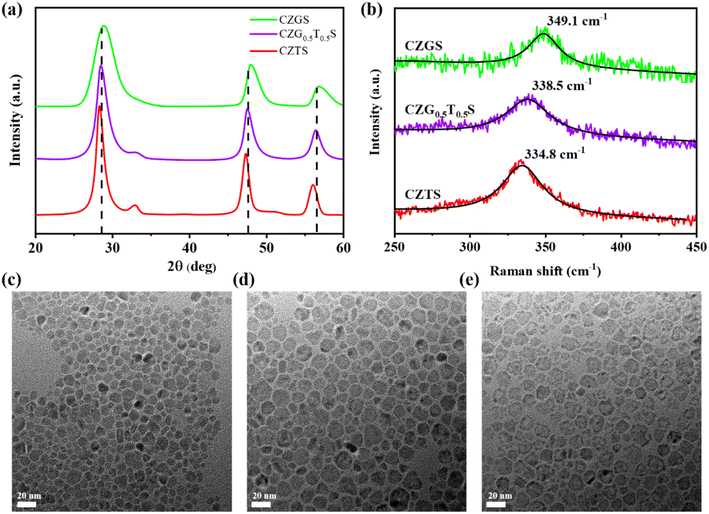 | ||
| Fig. 1 (a) XRD patterns and (b) Raman spectra for CZGxT1−xS samples. TEM morphologies of (c) CZTS, (d) CZG0.5T0.5S, and (e) CZGS samples. | ||
The CZTS and CZGS nanoparticles demonstrate typical Raman peaks in Fig. 1b at 334.8 cm−1 and 349.1 cm−1, respectively, which are consistent with previously reported Raman shifts for CZTS and CZGS samples.12,20 The CZG0.5T0.5S sample exhibits a Raman peak of 338.5 cm−1, which is located between the Raman peaks of CZTS and CZGS. This observation is consistent with previous reports, which have demonstrated that the main Raman peaks of the CZGxT1−xS samples are blueshifted with increasing Ge concentrations.12,14 No extra Raman peaks were detected in the three CZGxT1−xS samples, which confirms that our CZGxT1−xS nanoparticles are pure kesterite with tetragonal structures.
The morphologies and dispersibility of the CZGxT1−xS samples are presented in the TEM images in Fig. 1c–e. All the nanoparticles are roughly spherical, with particle sizes smaller than 20 nm. These nanoparticles show excellent dispersibility without any agglomeration, which is beneficial for forming well-dispersed nanoparticle ink and ensures the formation of uniform and compact CZGxT1−xS nanoparticle HTLs above the perovskite films. High-resolution TEM (HRTEM) characterizations of the CZGxT1−xS nanoparticles are presented in ESI Fig. S2.† The lattice distances of the CZGxT1−xS nanoparticles are estimated to be 3.33–3.13 Å from the lattice fringes, which correspond to the (112) crystal planes of the CZGxT1−xS nanoparticles and slightly decrease with increasing Ge concentrations.
The XPS survey spectra of the CZGxT1−xS nanoparticles are given in ESI Fig. S3.† The Cu, Zn, Ge, Sn, and S peaks are clearly detected, while Sn 3d and Ge 2p peaks are absent in the CZGS and CZTS nanoparticles, respectively. The exact compositions of the CZGxT1−xS nanoparticles are determined using Energy dispersive X-ray spectroscopy (EDS) and summarized in ESI Table S2.† The atomic ratios of Cu, Zn, Ge, Sn, and S are slightly different from their stoichiometric ratio, and this has been widely observed for CZTS and CZGS nanoparticles. However, the atomic ratios of Ge/(Ge + Sn) are 0.0, 0.22, 0.51, 0.74, and 1.0, which agree quite well with their nominal compositions.
The planar morphology of the FA1−xMAxPbI3−yBry perovskite film from a two-step deposition method is presented in Fig. S4†.21–23 Perovskite crystals with well-defined grain boundaries are clearly visible. The CZGxT1−xS nanoparticle HTLs are prepared via spin-coating the CZGxT1−xS nanoparticle ink and annealing at 100 °C in an ambient atmosphere.
The planar morphologies of the CZGxT1−xS nanoparticle HTLs are presented in Fig. 2a–c and ESI Fig. S5.† Clearly, the rough perovskite surface is planarized after the deposition of the CZGxT1−xS nanoparticle HTL, which is a prerequisite for the intimate contact with the subsequently blade-coated carbon electrode. Additionally, all three CZGxT1−xS nanoparticle HTLs are uniform without any obvious cracks or pinholes that could effectively separate the perovskite film from the carbon electrode. Thus, the carrier recombination at the C-PSCs can be suppressed, and superior PCEs can be demonstrated in our study. The compact and uniform characteristics of the CZGxT1−xS nanoparticle HTL are further demonstrated in the cross-sectional images in Fig. 2d–f. The CZGxT1−xS nanoparticles are completely and intimately capped on the perovskite films, and the HTLs exhibit film thicknesses of approximately 120 nm.
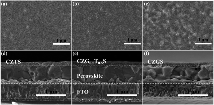 | ||
| Fig. 2 Planar and cross-sectional SEM images of (a and d) CZTS, (b and e) CZG0.5T0.5S, and (c and f) CZGS HTLs. | ||
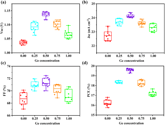
C-PSCs utilizing these CZGxT1−xS (x = 0, 0.25, 0.50, 0.75, and 1.0) nanoparticles as HTLs are fabricated according to our previous reports,10,11 and the photovoltaic performances are evaluated and summarized in Fig. 3a–d and Table S3.† Clearly, all the photovoltaic parameters, i.e., Voc, Jsc, FF, and PCE, are closely related to the composition of the CZGxT1−xS HTLs. The two reference CZTS and CZGS HTLs contributed to the C-PSCs with moderate average PCEs of 16.2% and 17.2%, respectively, which are consistent with the results from our previous reports.10,11 In contrast, the alloyed CZGxT1−xS HTLs (x = 0.25, 0.50, and 0.75) resulted in C-PSCs with greatly enhanced PCEs. The highest average PCE is 19.6%, which is demonstrated in C-PSCs with CZG0.5T0.5S as a HTL.
The champion C-PSCs with CZGxT1−xS HTLs are further studied. The corresponding J–V curves and the photovoltaic parameters of C-PSCs with the CZG0.5T0.5S HTL together with the reference CZTS and CZGS HTLs are presented in Fig. 4a and Table 1. The J–V curves of the C-PSCs with CZG0.25T0.75S and CZG0.75T0.25S HTLs are presented in ESI Fig. S6.† The highest PCEs for C-PSCs with CZTS and CZGS HTLs are 16.8% and 17.7%, respectively. When the alloyed CZG0.25T0.75S, CZG0.5T0.5S, and CZG0.75T0.25S nanoparticles are utilized as HTLs, the corresponding PCEs are greatly boosted to 18.6%, 19.8%, and 18.6% respectively. The enormously increased Voc (Voc = 1.138 V) compared with the two reference CZTS (Voc = 1.042 V) and CZGS (Voc = 1.084 V) HTLs is primarily responsible for the highest PCE for the corresponding C-PSC with CZG0.5T0.5S as the HTL, although the corresponding Jsc and FF are also slightly enhanced for the CZG0.5T0.5S HTL.
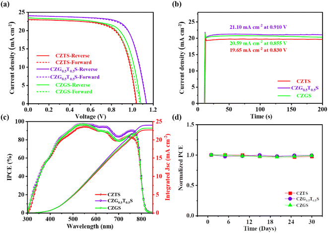 | ||
| Fig. 4 (a) J–V curves, (b) stable output curves, (c) IPCE spectra, and (d) device stability for the champion C-PSCs with CZTS, CZG0.5T0.5S, and CZGS HTLs. | ||
| V oc (V) | J sc (mA cm−2) | FF (%) | PCE (%) | |
|---|---|---|---|---|
| CZTS-reverse | 1.042 | 23.00 | 70.11 | 16.8 |
| CZTS-forward | 1.038 | 22.92 | 69.69 | 16.6 |
| CZG0.5T0.5S-reverse | 1.138 | 24.10 | 72.04 | 19.8 |
| CZG0.5T0.5S-forward | 1.140 | 24.10 | 71.05 | 19.5 |
| CZGS-reverse | 1.084 | 23.44 | 69.54 | 17.7 |
| CZGS-forward | 1.073 | 23.44 | 67.75 | 17.0 |
The PCEs from the reverse and forward scan measurements are only slightly different, which indicates that the J–V hysteresis phenomenon is negligible in our C-PSCs with CZGxT1−xS HTLs. The steady-state PCEs were also evaluated under standard AM 1.5 G illumination in Fig. 4b. The average output current densities are 19.65 mA cm−2, 20.59 mA cm−2, and 21.10 mA cm−2 for C-PSCs with CZTS, CZGS, and CZG0.5T0.5S HTLs, respectively. Correspondingly, the steady-state PCEs are 16.3%, 17.6%, and 19.2%, respectively, which agree quite well with the PCE values from the reversed J–V measurements.
The current densities extracted from the IPCE spectra in Fig. 4c are 22.67 mA cm−2, 23.15 mA cm−2, and 23.89 mA cm−2 for C-PSCs with CZTS, CZGS, and CZG0.5T0.5S HTLs, respectively, which are also consistent with those from J–V measurements. The stability of the C-PSCs with the CZGxT1−xS (x = 0, 0.5, and 1.0) HTLs is further evaluated in an ambient atmosphere with humidity at approximately 30%. Without capsulation, C-PSCs with the CZTS, CZGS, and CZG0.5T0.5S HTLs demonstrated excellent storage stability with negligible PCE decay after 30 days, as shown in Fig. 4d. This phenomenon was also demonstrated in our previous studies, and is attributed to the waterproof capability and excellent chemical stability of the CZGxT1−xS HTLs and the carbon electrode.10,11,15,24,25
The device structure of our C-PSCs is schematically depicted in Fig. 5a, which consists of fluorine-doped tin oxide (FTO), SnO2 electron transport layer (ETL), perovskite layer, CZGxT1−xS HTL, and carbon electrode in sequence. The ultraviolet photoelectron spectroscopy (UPS) spectra of CZTS, CZG0.5T0.5S, and CZGS are provided in Fig. S7.† The Fermi levels are determined to be −4.68 eV, −4.64 eV, and −4.77 eV for CZTS, CZG0.5T0.5S, and CZGS HTLs, respectively, and the corresponding valence band positions are calculated to be −5.23 eV, −5.23 eV, and −5.22 eV, respectively. The optical band gaps of CZTS, CZG0.5T0.5S, and CZGS are estimated using Tauc plots from the UV-vis absorbance, as shown in Fig. S8,† and the corresponding band gaps are 1.55 eV, 1.72 eV, and 1.85 eV, respectively. Therefore, the conduction band positions of CZTS, CZG0.5T0.5S, and CZGS are −3.68 eV, −3.51 eV, and −3.37 eV, respectively.
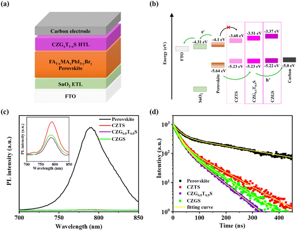 | ||
| Fig. 5 (a) Schematic device structure and (b) energy band alignment for our C-PSCs. (c) PL and (d) TRPL spectra for perovskite/CZGxT1−xS (x = 0, 0.5, and 1.0) films. | ||
According to first principles calculations, the valence band maximum of CZGxT1−xS mainly consists of Cu-d and S-p orbitals, whereas conduction band minimum consists of Ge or Sn-s orbitals and S-s orbitals. Thus, when more Ge is incorporated into CZGxT1−xS, the valence band maximum is nearly the same, while the conduction band minimum is significantly upshifted.26 The energy band alignment of our C-PSCs is depicted in Fig. 5b. The valence band of the CZGxT1−xS HTL is positioned between those of perovskite and the carbon electrode, and thus, a gradient energy band alignment is formed at the perovskite/CZGxT1−xS/carbon interface, which will facilitate hole transportation from the perovskite film to the carbon electrode. The conduction band energy barrier at the perovskite/CZGxT1−xS interface is enlarged from 0.42 eV for pure CZTS to 0.73 eV for pure CZGS.
The smallest conduction band energy barrier (0.42 eV) for the perovskite/CZTS interface might not be sufficiently large to effectively inhibit the backward electron transfer from the perovskite to CZTS HTL, and thus, moderate charge carrier recombination at the perovskite/CZTS interface continues to exist. When Ge is alloyed into CZTS, the obtained CZGxT1−xS (x = 0.5 and 1.0) HTL exhibits an enlarged optical band gap. Therefore, the conduction band energy barrier for perovskite/CZGxT1−xS could be increased, which could contribute to largely suppressed charge carrier recombination at the perovskite/CZGxT1−xS interface. Thus, a superior Voc and PCE for the C-PSCs with CZGxT1−xS (x = 0.5 and 1.0) HTLs are observed in our study.
The photoluminescence (PL) spectra of the perovskite/CZGxT1−xS films are presented in Fig. 5c. For the reference perovskite film without the CZGxT1−xS HTL, a characteristic PL peak at approximately 790 nm was observed. When CZGxT1−xS HTLs are capped onto the perovskite films, the PL intensities are enormously quenched, which originates from the fast hole transfer from perovskite to the CZGxT1−xS HTL due to the suitable energy band alignment at the perovskite/CZGxT1−xS interface.27,28
The magnified PL spectra of the perovskite/CZGxT1−xS films are further presented in the inset of Fig. 5c. Clearly, the perovskite/CZG0.5T0.5S film demonstrates the lowest PL intensity, indicating that the CZG0.5T0.5S HTL exhibits superior hole extraction capability compared with the reference CZTS and CZGS HTLs. This idea is further confirmed by the time-resolved photoluminescence (TRPL) spectra in Fig. 5d. The average decay time for perovskite film is 250.5 ns, which is enormously decreased to 40.1–56.0 ns after a CZGxT1−xS HTL is deposited onto the perovskite film (the details are summarized in Table S4†). Among the three CZGxT1−xS HTLs, CZG0.5T0.5S contributed the shortest average decay time compared with the other two reference CZTS and CZGS HTLs.27–29
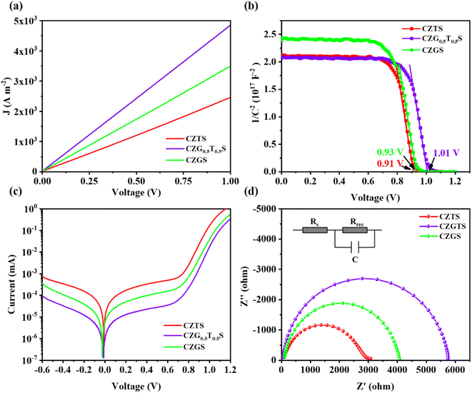
Conductivity values of the CZGxT1−xS HTLs are estimated from their current density–voltage (J–V) curves using a FTO/CZGxT1−xS/carbon device and presented in Fig. 6a. The calculated conductivity values are 2.93 × 10⁻⁴ S m−1, 5.80 × 10⁻⁴ S m−1, and 4.17 × 10⁻⁴ S m−1 for the CZTS, CZG0.5T0.5S, and CZGS HTLs, respectively, after fitting the linear part of the J–V curves between 0.0 V and 0.5 V. The carrier mobilities of the CZGxT1−xS HTLs were estimated using Mott–Gurney equation J = 9ε0εμV2/(8L3), where μ denotes the hole mobility. After fitting the linear part of J1/2 V curves between 0.5 V and 1.0 V in ESI Fig. S9,† the hole mobilities are calculated to be 2.30 × 10⁻⁴ cm2 V−1 s−1, 4.27 × 10⁻⁴ cm2 V−1 s−1, and 3.14 × 10⁻⁴ cm2 V−1 s−1 for CZTS, CZG0.5T0.5S, and CZGS HTLs, respectively.
Previous studies have also demonstrated that Ge-doped CZTS exhibited superior hole mobilities,12,14 which are consistent with our observations and could partially contribute to the enhanced conductivity of the CZG0.5T0.5S HTL. It is also likely that the enlarged CZG0.5T0.5S crystal sizes in Fig. 1c–e could be a possible contributor to the enhanced conductivity and mobility of the corresponding CZG0.5T0.5S HTL. Therefore, the CZG0.5T0.5S HTL, which exhibited the highest conductivity, could transport the holes from the perovskite film to the carbon electrode in the most efficient manner compared with CZTS and CZGS HTLs, which might contribute to the highest Jsc values in the C-PSCs with CZG0.5T0.5S HTLs.
The built-in potential plays a vital role in the dissociation of photo-generated carriers and their transportation towards the ETL and HTL. The built-in potentials are evaluated to be 0.91 V, 0.93 V, and 1.01 V for the C-PSCs with the CZTS, CZGS, and CZG0.5T0.5S HTLs, respectively, as shown in Fig. 6b. The largest built-in potential in C-PSCs with the CZG0.5T0.5S HTL would contribute to the most efficient carrier dissociation and transportation towards the ETL and HTL, which also contributes to the highest Jsc and Voc in the corresponding C-PSCs.30–32 The dark current of the C-PSCs with CZGxT1−xS HTLs (x = 0, 0.5, and 1.0) is presented in Fig. 6c. The highest built-in potential in C-PSCs and hole mobility associated with the CZG0.5T0.5S HTL facilitated the most efficient hole transportation across the HTL, and thus, carrier accumulation at the perovskite/HTL interface is elevated. However, the CZG0.5T0.5S HTL ensures a sufficiently large energy barrier at the conduction band of the perovskite/CZG0.5T0.5S interface, which effectively suppressed the charge carrier recombination. Therefore, the C-PSC with the CZG0.5T0.5S HTL exhibited the smallest dark current due to its lowest charge carrier recombination rate in the C-PSC.33,34
After fitting the electrochemical impedance spectroscopy (EIS) spectra at 1.0 V in the dark with the corresponding equivalent circuit in Fig. 6d, the recombination resistances for C-PSCs are calculated to be 2687 Ω, 3914 Ω, and 5637 Ω for the CZTS, CZGS, and CZG0.5T0.5S HTLs, respectively. Clearly, the C-PSC with the CZG0.5T0.5S HTL exhibits the largest recombination resistance, which further confirmed that the charge carrier recombination rate in the corresponding C-PSC is the lowest among the three CZGxT1−xS (x = 0, 0.5, and 1.0) HTLs.32,35
3 Conclusion
CZGxT1−xS nanoparticles were synthesized with different Ge concentrations (x = 0, 0.25, 0.50, 0.75, and 1.0). The synthesized CZGxT1−xS nanoparticles exhibited pure kesterite phase with particle sizes smaller than 20 nm, which could be well dispersed to form CZGxT1−xS nanoparticle ink. C-PSCs with these CZGxT1−xS nanoparticle HTLs were fabricated, and their performances were closely related to the composition of the CZGxT1−xS HTLs. The optimum CZG0.5T0.5S HTL contributed to C-PSCs with a champion PCE of 19.8%, which mainly originated from the ideal hole extraction capability of the CZG0.5T0.5S HTL and the lowered charge carrier recombination at the perovskite/CZG0.5T0.5S interface. The obtained PCE for the C-PSC with the CZG0.5T0.5S HTL was much higher than those from previous reports with pure CZTS and CZGS HTLs. Thus, the proposed composition engineering strategy might be a prospective method to further promote the PCEs of C-PSCs with CZTS or CZGS inorganic HTLs in the future.Data availability
The data supporting this article have been included as part of the ESI.†Author contributions
Nian Cheng: conceptualization, investigation, writing – original draft, writing – review and editing. Weiwei Li: visualization, methodology, investigation, writing – review and editing. Zhenyu Xiao: methodology, investigation, writing – review and editing. Han Pan: visualization, methodology, investigation. Dingshan Zheng: validation, visualization, writing – review and editing. Wen-Xing Yang: resources, supervision, writing – review and editing.Conflicts of interest
There are no conflicts to declare.Acknowledgements
This work is supported by the National Natural Science Foundation of China (Grant No. 12075036 and 12375008), the Foundation for Innovation Research Groups of the Hubei Natural Science Foundation of China (No. 2023AFA025), the Young Fund of the Natural Science Foundation of Hubei Province of China (No. 2024AFB430), and the Key Research Program of University in Henan Province (No. 23A140006). The authors also thank Zhenyu Xiao, Zongwen Zhang, Dongli Xu, Yanping Xie, and Peiyin Guo from the Analysis & Testing Center at Xinyang Normal University for the material characterizations.References
- D. Bogachuk, S. Zouhair, K. Wojciechowski, B. Yang, V. Babu, L. Wagner, B. Xu, J. Lim, S. Mastroianni, H. Pettersson, A. Hagfeldt and A. Hinsch, Low-temperature carbon-based electrodes in perovskite solar cells, Energy Environ. Sci., 2020, 13(11), 3880–3916 RSC.
- X. Zhang, Z. Yu, D. Zhang, Q. Tai and X. Z. Zhao, Recent Progress of Carbon-Based Inorganic Perovskite Solar Cells: From Efficiency to Stability, Adv. Energy Mater., 2022, 13(33), 2201320 CrossRef.
- T. Du, S. Qiu, X. Zhou, V. M. Le Corre, M. Wu, L. Dong, Z. Peng, Y. Zhao, D. Jang, E. Spiecker, C. J. Brabec and H.-J. Egelhaaf, Efficient, stable, and fully printed carbon-electrode perovskite solar cells enabled by hole-transporting bilayers, Joule, 2023, 7(8), 1920–1937 CrossRef CAS.
- E. C. Kohlrausch, D. de Vasconcelos Freitas, C. I. da Silva Filho, L. L. Fernandes, L. A. Santa-Cruz, L. J. Lins Maciel, M. Z. Oliveira, C. I. d. L. dos Santos and G. Machado, Advances in Carbon Materials Applied to Carbon-Based Perovskite Solar Cells, Energy Technol., 2023, 11(4), 2200676 CrossRef CAS.
- C. Zhang, S. Liang, W. Liu, F. T. Eickemeyer, X. Cai, K. Zhou, J. Bian, H. Zhu, C. Zhu, N. Wang, Z. Wang, J. Zhang, Y. Wang, J. Hu, H. Ma, C. Xin, S. M. Zakeeruddin, M. Grätzel and Y. Shi, Ti1–graphene single-atom material for improved energy level alignment in perovskite solar cells, Nat. Energy, 2021, 6(12), 1154–1163 CrossRef CAS.
- Y. Wang, W. Li, Y. Yin, M. Wang, W. Cai, Y. Shi, J. Guo, W. Shang, C. Zhang, Q. Dong, H. Ma, J. Liu, W. Tian, S. Jin, J. Bian and Y. Shi, Defective MWCNT Enabled Dual Interface Coupling for Carbon-Based Perovskite Solar Cells with Efficiency Exceeding 22%, Adv. Funct. Mater., 2022, 32(31), 2204831 CrossRef CAS.
- J. S. Shaikh, N. S. Shaikh, Y. K. Mishra, P. Kanjanaboos, P. M. Shewale, S. Sabale, S. Praserthdam and C. D. Lokhande, Low-cost Cu-based inorganic hole transporting materials in perovskite solar cells: Recent progress and state-of-art developments, Mater. Today Chem., 2021, 20, 100427 CrossRef CAS.
- T. Ye, X. Sun, X. Zhang and S. Hao, Recent advances of Cu-based hole transport materials and their interface engineering concerning different processing methods in perovskite solar cells, J. Energy Chem., 2021, 62, 459–476 CrossRef CAS.
- G. M. Arumugam, S. K. Karunakaran, C. Liu, C. Zhang, F. Guo, S. Wu and Y. Mai, Inorganic hole transport layers in inverted perovskite solar cells: A review, Nano Sel., 2021, 2(6), 1081–1116 CrossRef CAS.
- Y. Cao, W. Li, Z. Liu, Z. Zhao, Z. Xiao, W. Zi and N. Cheng, Ligand modification of Cu2ZnSnS4 nanoparticles boosts the performance of low temperature paintable carbon electrode based perovskite solar cells to 17.71%, J. Mater. Chem. A, 2020, 8(24), 12080–12088 RSC.
- N. Cheng, Z. Liu, W. Li, Z. Yu, B. Lei, W. Zi, Z. Xiao, S. Sun, Z. Zhao and P.-A. Zong, Cu2ZnGeS4 as a novel hole transport material for carbon-based perovskite solar cells with power conversion efficiency above 18%, Chem. Eng. J., 2023, 454, 140146 CrossRef CAS.
- D. Mora-Herrera, M. Pal and F. Paraguay-Delgado, Facile solvothermal synthesis of Cu2ZnSn1-xGexS4 nanocrystals: Effect of Ge content on optical and electrical properties, Mater. Chem. Phys., 2021, 257, 123764 CrossRef CAS.
- G. M. Ford, Q. Guo, R. Agrawal and H. W. Hillhouse, Earth Abundant Element Cu2Zn(Sn1−xGex)S4 Nanocrystals for Tunable Band Gap Solar Cells: 6.8% Efficient Device Fabrication, Chem. Mater., 2011, 23(10), 2626–2629 CrossRef CAS.
- F. Enrique Cancino-Gordillo, J.-L. Ortiz-Quiñonez, M. Pal, G. R. Silva and U. Pal, Removal of secondary phases and its effect on the transport behavior of Cu2ZnSn1−xGexS4 kesterite nanoparticles, Appl. Surf. Sci., 2023, 617, 156617 CrossRef CAS.
- Z. Liu, Z. Yu, W. Li, Z. Zhao, Z. Xiao, B. Lei, W. Zi, N. Cheng, J. Liu and Y. Tu, Scalable one-step heating up synthesis of Cu2ZnSnS4 nanocrystals hole conducting materials for carbon electrode based perovskite solar cells, Sol. Energy, 2021, 224, 51–57 CrossRef CAS.
- R. Caballero, I. Victorov, R. Serna, J. M. Cano-Torres, C. Maffiotte, E. Garcia-Llamas, J. M. Merino, M. Valakh, I. Bodnar and M. León, Band-gap engineering of Cu2ZnSn1−xGexS4 single crystals and influence of the surface properties, Acta Mater., 2014, 79, 181–187 CrossRef CAS.
- T. G. Sanchez, E. Regalado-Pérez, X. Mathew, M. F. Sanchez, Y. Sanchez, E. Saucedo and N. R. Mathews, Ge doped Cu2ZnSnS4: An investigation on absorber recrystallization and opto-electronic properties of solar cell, Sol. Energy Mater. Sol. Cells, 2019, 198, 44–52 CrossRef CAS.
- F. E. Cancino-Gordillo, J. V. Cab and U. Pal, Structure and transport behavior of hydrothermally grown phase pure Cu2ZnSn1−xGexS4 (x = 0.0, 0.3) nanoparticles, Appl. Surf. Sci., 2022, 571, 151261 CrossRef CAS.
- D. Mora-Herrera, S. Shaji and M. Pal, Ge incorporation in kesterite thin films by solution processing route: An in-depth study of structural and optoelectronic properties, J. Alloys Compd., 2022, 921, 166184 CrossRef CAS.
- E. Garcia-Llamas, M. Guc, I. V. Bodnar, X. Fontané, R. Caballero, J. M. Merino, M. León and V. Izquierdo-Roca, Multiwavelength excitation Raman scattering of Cu2ZnSn1−xGex(S,Se)4 single crystals for earth abundant photovoltaic applications, J. Alloys Compd., 2017, 692, 249–256 CrossRef CAS.
- N. Cheng, W. Li, D. Zheng and W. X. Yang, Surface Passivation of Perovskite Solar Cells with Oxalic Acid: Increased Efficiency and Device Stability, ChemPlusChem, 2023, 88(10), 202300367 CrossRef PubMed.
- N. Cheng, W. Li, D. Zheng and W. X. Yang, Simultaneous Incorporation of CsI in the Two-step Deposition Process Boosts the Power Conversion Efficiency and Stability of Perovskite Solar Cells, ChemPhysChem, 2023, 25(3), e202300599 CrossRef PubMed.
- N. Cheng, W. Li, D. Zheng and W.-X. Yang, Enhance the efficiency of perovskite solar cells using W doped SnO2 electron transporting layer, ChemPhotoChem, 2024, 8, 202300275 CrossRef.
- Y. Cao, H. Wu, W. Li, Z. Zhao, Z. Xiao, W. Zi, N. Cheng, J. Liu and Y. Tu, Cu2ZnSnS4 as an efficient hole transporting material for low temperature paintable carbon electrode based perovskite solar cells, Org. Electron., 2020, 76, 105455 CrossRef CAS.
- Z. Yu, W. Li, N. Cheng, Z. Liu, B. Lei, Z. Xiao, W. Zi, Z. Zhao and Y. Tu, Cu2SnS3 Nanocrystal-Based Hole-Transport Layer for Carbon Electrode-Based Perovskite Solar Cells, ACS Appl. Nano Mater., 2022, 5(8), 10755–10762 CrossRef CAS.
- Q. Liu, Z. Cai, D. Han and S. Chen, Natural Intermediate Band in I2-II-IV-VI4 Quaternary Chalcogenide Semiconductors, Sci. Rep., 2018, 8(1), 1604 CrossRef PubMed.
- X. Cui, J. Jin, Z. Zhu, T. Guo, Q. Tang, Y. Zhou, L. Li, Z. Wang, G. Tang and Q. Tai, Low-temperature solution-processed LaNiO3 hole-transport layer for UV-stable inverted perovskite solar cells, Chem. Commun., 2023, 59(50), 7787–7790 RSC.
- J. Zhang, S. Zhu, Q. Yang, C. Gao and X. Liu, Copper-Doped InxGa2-xO3 Nanocrystals as Efficient Hole Transport Materials of Perovskite Solar Cells by Regulating Energy Levels, Sol. RRL, 2023, 7(14), 2300263 CrossRef CAS.
- H. Pan, Y. Zheng, W. He, W. Yang, X. Gong, X. Liu, Q. Wei, Y. Liu, Y. Shen and M. Wang, Molecular interaction modulating Ruddlesden–Popper tin-based perovskite crystallization, J. Mater. Chem. A, 2023, 11(19), 10319–10327 RSC.
- Z. Liu, T. Liu, M. Li, T. He, G. Guo, P. Liu, T. Chen, J. Yang, C. Qin, X. Dai and M. Yuan, Eliminating Halogen Vacancies Enables Efficient MACl-Assisted Formamidine Perovskite Solar Cells, Advanced Science, 2024, 11, 2306280 CrossRef CAS PubMed.
- K. Liu, Y. Luo, Y. Jin, T. Liu, Y. Liang, L. Yang, P. Song, Z. Liu, C. Tian, L. Xie and Z. Wei, Moisture-triggered fast crystallization enables efficient and stable perovskite solar cells, Nat. Commun., 2022, 13(1), 4891 CrossRef CAS PubMed.
- H. Guo, W. Xiang, Y. Fang, J. Li and Y. Lin, Molecular Bridge on Buried Interface for Efficient and Stable Perovskite Solar Cells, Angew. Chem., Int. Ed., 2023, 62(34), 202304568 CrossRef PubMed.
- Y. Tu, G. Li, J. Ye, C. Deng, R. Liu, G. Yang, T. Shao, Y. Li, Y. Zang, Y. Wang, Q. Zhou, J. Wu and W. Yan, Multifunctional Imidazolidinyl Urea Additive Initiated Complex with PbI2 Toward Efficient and Stable Perovskite Solar Cells, Small, 2024, 20, 2309033 CrossRef CAS PubMed.
- J. Duan, Y. Zhao, X. Yang, Y. Wang, B. He and Q. Tang, Lanthanide Ions Doped CsPbBr3 Halides for HTM-Free 10.14%-Efficiency Inorganic Perovskite Solar Cell with an Ultrahigh Open-Circuit Voltage of 1.594 V, Adv. Energy Mater., 2018, 8(31), 1802346 CrossRef.
- R. Lu, Y. Liu, D. Zhao, X. Guo and C. Li, Stabilizing black-phase FAPbI3 in humid air with secondary ammoniums, J. Mater. Chem. A, 2022, 10(40), 21422–21429 RSC.
Footnote |
| † Electronic supplementary information (ESI) available: the Experimental section, XRD patterns, HRTEM images, XPS spectra, planar SEM image, champion J–V curves, UPS spectra, Tauc plots, and Tables S1–S4 are provided. See DOI: https://doi.org/10.1039/d4ta07106a |
| This journal is © The Royal Society of Chemistry 2025 |

