
 Open Access Article
 This Open Access Article is licensed under a
 Creative Commons Attribution 3.0 Unported Licence
Hybrid SnO2/g-C3N4 layers with plasma-induced modifications for enhanced charge transport in perovskite solar cells†
Minwoo
Lee
 a,
Elisa Yun
Mei Ang
b,
William
Toh
c,
Peng Cheng
Wang
b,
Teng Yong
Ng
c,
So Young
Lee
d,
Sun-woo
Kim
d,
Martin A.
Green
a,
Xiaojing
Hao
*a,
Jae Sung
Yun
*ae and
Dong Han
Seo
*d
a,
Elisa Yun
Mei Ang
b,
William
Toh
c,
Peng Cheng
Wang
b,
Teng Yong
Ng
c,
So Young
Lee
d,
Sun-woo
Kim
d,
Martin A.
Green
a,
Xiaojing
Hao
*a,
Jae Sung
Yun
*ae and
Dong Han
Seo
*d
aAustralian Centre for Advanced Photovoltaics (ACAP), School of Photovoltaic and Renewable Energy Engineering, University of New South Wales, Sydney, NSW 2052, Australia. E-mail: xj.hao@unsw.edu.au
bEngineering Cluster, Singapore Institute of Technology, 10 Dover Drive, Singapore 138683, Singapore
cSchool of Mechanical and Aerospace Engineering, Nanyang Technological University, 50 Nanyang Avenue, Singapore, 639798, Singapore
dEnergy Materials & Devices, Korea Institute of Energy Technology (KENTECH), Naju, Jeollanam-do 58330, Republic of Korea. E-mail: dhseo@kentech.ac.kr
eDepartment of Electrical and Electronic Engineering, Advanced Technology Institute (ATI), University of Surrey, Guildford, Surrey GU2 7XH, UK. E-mail: j.yun@surrey.ac.uk
First published on 3rd March 2025
Abstract
The design of high-performance perovskite solar cells (PSCs) for indoor applications requires precise interface engineering to optimize charge extraction, particularly under low-light intensity conditions, where excess carrier density is limited. To enhance the charge extraction properties in PSCs, various carbon-based nanomaterials with varying functional groups have been utilized as electron transport layer (ETL) additives to address the issue with limited success. Thereby, in this work, we introduce a plasma-modified graphitic carbon nitride (GCN_PT) as an ETL interface layer additive which is deposited onto the SnO2 electron transport layer to enhance electron extraction. Plasma modification transforms randomly distributed GCN particles (200–500 nm) into uniformly sized nanoparticles (1–3 nm) while inducing partial graphitization, significantly improving conductivity and charge transport properties. These modifications enable more efficient extraction and transport of photogenerated carriers at the SnO2/GCN_PT interface, substantially enhancing short-circuit current density (JSC). This improvement is particularly pronounced under low-light indoor conditions, where reduced photon flux limits carrier generation within the perovskite layer. Notably, under 1000 lux indoor white LED illumination, the optimized SnO2/GCN_PT interface achieves a power conversion efficiency of approximately 39.80%, demonstrating its potential to advance indoor photovoltaic applications through enhanced JSC and interface optimization.
Introduction
Perovskite solar cells (PSCs) have emerged as a revolutionary photovoltaic technology, achieving power conversion efficiencies (PCE) exceeding 26% in single-junction devices.1 This rapid progress is attributed to the exceptional optoelectronic properties of metal halide perovskites (PVSK), such as a tunable bandgap, high absorption coefficients, and long carrier diffusion lengths.2 Despite these advancements, further enhancement of PCE is required to compete with established photovoltaic technologies and to address challenges such as non-radiative recombination and stability under operational conditions.Various strategies have been employed to improve the efficiency of PSCs, focusing on mitigating the inherent challenges posed by structural imperfections in PVSK materials. Composition engineering has been extensively explored to improve the structural and phase stability of PVSK materials.3 The incorporation of mixed cations, such as formamidinium (FA), cesium (Cs), and methylammonium (MA), or mixed halides (e.g., iodide and bromide), has proven effective in stabilizing the desirable black-phase PVSK structure while reducing defect density.3–5 Additionally, the use of additive materials such as methylammonium chloride (MACl),6 phenylethylammonium chloride (PACl),7 and zwitterionic acetylcholine cation (AC+) and Cl− anions (AACl)8 has been shown to control the intermediate phases of PVSK crystallization. These additives prevent the formation of the undesirable δ-phase and promote the stable α-phase of the PVSK structure, resulting in improved crystal quality, reduced bulk defect density, enhanced phase stability, and higher PCE. Moreover, light management techniques have contributed significantly to improving PSC performance. The incorporation of anti-reflective coatings9 and textured substrates10 has enhanced light harvesting, reducing optical losses and increasing JSC.
Another approach includes interface engineering, which has been widely implemented to optimize charge extraction and minimize energy losses at the interfaces between the PVSK absorber and the charge transport layers.11–13 These energy losses are largely attributed to the presence of vacancies and defect sites within the PVSK structure, which promote non-radiative recombination. One effective approach involves the use of two-dimensional (2D) long-chain cations, which passivate both the top and bottom surfaces of the PVSK layer by forming ultra-thin layers of 2D PVSKs.14–16 This passivation significantly reduces defect sites, suppresses non-radiative recombination, and enhances the stability of PSCs.
As an alternative to 2D perovskites, carbon-based nanomaterials have been explored as passivation layers to mediate defects at the interface between the perovskite layer and the electron transport layer (ETL). These include graphene,17 modified graphene-based materials, and more recently, graphitic carbon nitride (GCN).18–20 Such strategies address critical performance-limiting factors in PSCs, significantly enhancing efficiency, stability, and overall device performance.
In this work, we introduce a novel approach to interface engineering by employing plasma-treated GCN (GCN_PT) as an interfacial layer between the SnO2 ETL and the PVSK absorber. Plasma treatment of GCN in the liquid phase transforms bulk, randomly distributed GCN particles/sheets into size uniform GCN nanoparticles (1–3 nm), facilitating even and homogenous particle distribution in the ETL. Moreover, plasma treatment of GCN significantly alters its chemical and structural properties, including enhanced conductivity and improved interaction with the SnO2 layer. These modifications optimize the SnO2/GCN_PT interface, facilitating efficient charge transport and reducing energy losses. This interface engineering approach demonstrates the potential of plasma-modified materials to enhance the performance of perovskite solar cells, achieving a power conversion efficiency of approximately 39.80% under indoor white LED illumination (1000 lux).
Results and discussion
Fig. 1 illustrates the plasma modification process for modifying the GCN powder. The GCN was synthesized through thermally driven process (details in the experimental section) and dispersed in deionized water using a bath sonication to achieve a suspension of randomly oriented and sized particles/nanosheets. The dispersion was then subjected to low-temperature atmospheric pressure plasma treatment in the liquid phase, where electrons and radicals and active species generated by the plasma process,21 (OH*, NO*, , O3, N, O, e−) which effectively exfoliated and fragmented the GCN nanosheets into smaller size uniform nanoparticles which were dispersed in a solution. The treated dispersion, as shown in the schematic and vial images, exhibited a clear and transparent solution, indicating significant size reduction has occurred along with a more stable suspension was achieved compared to untreated GCN. In addition to size reduction, plasma treatment facilitated the incorporation of functionalized components within the dispersion. Optical emission spectroscopy detected the formation of NOX and OH species during plasma treatment, while ion chromatography analysis confirmed the presence of NO2 and NO3 in the GCN_PT dispersion sample (Fig. S1a and b†). This surface functionalization enhances the dispersibility of GCN in water and improving suspension stability. Plasma treatment also introduced surface modifications on GCN, including the transformation of the triazine structure into the graphitic structure with possible oxygen species incorporation, which improved the electrical conductivity as well as providing an anchoring site for the defect sites in the SnO2 layers, ultimately tailoring the physicochemical properties of GCN. This novel and scalable surface modification approach via liquid phase, low-temperature atmospheric pressure plasma treatment not only refines the particle size but also optimizes the material's electrical and surface properties, making it highly suitable for applications such as interfacial layers in perovskite solar cells.
 | ||
| Fig. 1 Schematic illustration of the modifying GCN powder by plasma treatment method. | ||
After the modification of the GCN by plasma treatment, scanning electron microscopy (SEM) was performed to evaluate the size and morphology of the GCN material before and after plasma treatment. Dispersion of untreated GCN typically consists of nanosheets with lateral dimensions ranging from several to hundreds of nanometers. However, GCN is prone to aggregation due to its hydrophilic surface functional groups (e.g., amino and imine groups), which provide moderate dispersion in water but are insufficient for long-term stabilization. The limited hydrophilicity, compared to materials with more polar or ionic surfaces, allows significant aggregation over time. Aggregation is primarily driven by van der Waals interactions and π–π stacking between layers or particles, especially for nanosheets with high surface energy. As a result, external interventions such as sonication are required to temporarily disperse GCN in water and reduce aggregation by breaking apart particle clusters. While sonication improves dispersion initially, GCN particles tend to re-aggregate over time, forming larger clusters due to insufficient electrostatic stabilization. In addition, without surfactants or stabilizing agents, dispersion stability remains limited. Fig. 2a presents SEM images of GCN drop-cast onto a substrate, revealing aggregated particles with sizes exceeding 100 nm. In contrast, the plasma-treated g-C3N4 (GCN_PT) shown in Fig. 2b exhibits a uniform morphology with significantly smaller and more finely distributed particles. Furthermore, HR-TEM images in Fig. S2a and b† confirm that GCN nanosheets, highlighted by blue arrows, exhibit lateral dimensions much larger than the 20 nm scale bar, consistent with the aggregation observed in SEM images (approximately 100 nm). For GCN_PT (Fig. S2c and d†), the TEM images show uniformly distributed black dots across the sample, with magnified views in Fig. S2d† revealing nanoparticle sizes below 5 nm. The observed lattice fringes further confirm the successful formation of well-defined GCN_PT nanoparticles.
 | ||
| Fig. 2 (a and b) SEM images of GCN and GCN_PT, respectively. (c) DLS particle size distribution data for GCN and GCN_PT. (d and e) XPS N 1s and C 1s spectra of GCN and GCN_PT powders. (f) MD simulation results of plasma bombardment on a GCN layer. | ||
Dynamic light scattering (DLS) was conducted on both GCN and GCN_PT samples dispersed in water to assess the particle size quantitatively. The samples were pre-filtered to remove large aggregates. The DLS results (Fig. 2c) demonstrate that GCN_PT has a dominant peak at approximately 1 nm, confirming the successful particle size reduction by plasma treatment. In comparison, the GCN sample exhibits a broad size distribution, ranging from 0.7 nm to 20 nm, indicating significant heterogeneity and aggregation in the untreated GCN. These findings confirm that the plasma treatment method effectively reduces the particle size of GCN and improves its dispersion behavior.
We conducted the XPS to analyze the chemical bond change before and after plasma treatment for GCN samples. The plasma treatment of GCN leads to significant changes in the N 1s and C 1s spectra, indicating structural and chemical modifications. In the N 1s spectra, as shown in Fig. 2d, the GCN_PT sample shows the decrease in the C![[double bond, length as m-dash]](https://www.rsc.org/images/entities/char_e001.gif) NC peak intensity (∼398.2 eV) reflects the formation of nitrogen vacancies, while the shift to higher binding energy (∼398.4 eV) suggests changes in the chemical environment, such as increased electron-withdrawing effects and disrupted π-conjugation due to nitrogen removal. Correspondingly, the C 1s spectra (Fig. 2e) show that GCN_PT sample has a low C–NHx peak (∼285–286 eV) and an increase in the sp2 peak (∼284.5 eV) compared to GCN, confirming partial graphitization and the partial conversion of CN bonds to CC bonds. These nitrogen vacancies and increased sp2 carbon content enhance the material's conductivity by reducing charge-trapping sites, improving π-electron transport, and facilitating charge transfer, encouraging favorable electron transport.
NC peak intensity (∼398.2 eV) reflects the formation of nitrogen vacancies, while the shift to higher binding energy (∼398.4 eV) suggests changes in the chemical environment, such as increased electron-withdrawing effects and disrupted π-conjugation due to nitrogen removal. Correspondingly, the C 1s spectra (Fig. 2e) show that GCN_PT sample has a low C–NHx peak (∼285–286 eV) and an increase in the sp2 peak (∼284.5 eV) compared to GCN, confirming partial graphitization and the partial conversion of CN bonds to CC bonds. These nitrogen vacancies and increased sp2 carbon content enhance the material's conductivity by reducing charge-trapping sites, improving π-electron transport, and facilitating charge transfer, encouraging favorable electron transport.
The molecular dynamics (MD) simulation results strongly align with the XPS data for GCN and GCN_PT, offering a mechanistic explanation for the plasma-induced modifications, as shown in Fig. S3 and S4† and the schematic of the simulation in Fig. 2f. The simulations demonstrate that plasma bombardment with  and
and  radicals break C–N bonds, leading to structural fragmentation and nitrogen vacancies, particularly at higher electric field strengths (>5 V Å−1), resulting in the formation of nitrogen vacancies and a carbon-rich surface. This finding corresponds well with the decreased intensity of the CNC peak (∼398.2 eV) and its shift to higher binding energy (∼398.4 eV) observed in the N 1s spectra of GCN_PT. Furthermore, the simulations reveal that
  and oxygen based radical species are highly reactive, suggesting possible oxygen incorporation during plasma treatment.22 This is supported by the increased peak near ∼286–287 eV in the C 1s spectra, which indicates the formation of C–O bonds. Therefore, these results provide a cohesive understanding of the structural and chemical transformations induced by plasma treatment.
A strong correlation with improved electrical properties was expected after confirming graphitization and chemical bonding changes in GCN_PT samples. To investigate this, we prepared thin films of GCN and GCN_PT by spin-coated on SnO2/ITO substrates, commonly used in the n-i-p structure of PVSK solar cells. The GCN_PT layer exhibited a compact and uniform morphology, while the GCN layer showed the presence of more extensive, non-uniform particles on the SnO2 layer, as shown in Fig. S5.†
To evaluate the electrical properties at the nanoscale, Kelvin Probe Force Microscopy (KPFM) measurements were performed for SnO2, GCN, and GCN_PT layers (Fig. 3a–c). The KPFM images reveal the contact potential difference (CPD) uniformity of the layers. Morphological images (Fig. S6†) show the root mean square (RMS) roughness values for SnO2 (7.44 nm), GCN (4.25 nm), and GCN_PT (4.15 nm). As depicted in Fig. 3d, GCN_PT exhibited the most homogeneous CPD distribution (3.90), significantly lower than SnO2 (7.53) and GCN (5.21). The uniform CPD distribution indicates fewer defect sites, which is crucial for minimizing recombination during charge transport in PVSK solar cells. Furthermore, the CPD of GCN_PT (∼525 mV) was notably shifted to higher values compared to SnO2 and GCN, suggesting that the work function of GCN_PT is closer to the conduction band. This indicates a more electron-rich surface, enhancing its suitability for the n-i-p structure of PVSK solar cells.
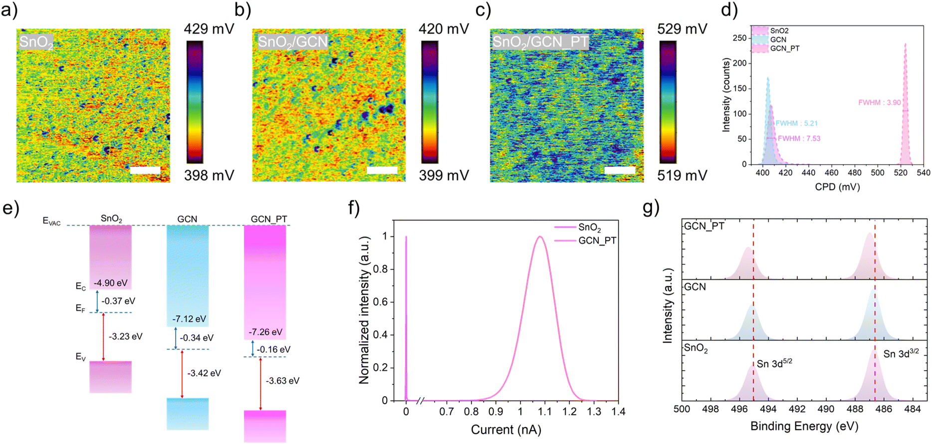 | ||
| Fig. 3 (a–c) CPD images of SnO2, SnO2/GCN, and SnO2/GCN_PT, respectively (scale bar: 500 nm). (d) CPD distributions for the three conditions. (e) Schematic band energy diagram of SnO2, GCN, and GCN_PT layers. (f) c-AFM measurements comparing the conductivity of SnO2 and GCN_PT. (g) XPS Sn 3d spectra of SnO2, GCN, and GCN_PT samples. | ||
To confirm the work function shift and band alignment, ultraviolet photoelectron spectroscopy (UPS) was conducted for SnO2, GCN, and GCN_PT layers (Fig. 3e). The results show that the work function of GCN_PT (0.16 eV) is significantly lower than that of SnO2 (0.37 eV) and GCN (0.34 eV). Additionally, the bandgap of each sample was determined from UV-vis spectroscopy (Fig. S7†), showing that the absorption of SnO2 is slightly lower than that of GCN and GCN_PT. Notably, the absorption profile of GCN_PT remains unchanged compared to GCN. This shift of work function corroborates the enhanced electron-rich surface observed in KPFM measurements. Additionally, conductive atomic force microscopy (c-AFM) was performed to assess the conductivity of the SnO2 and GCN_PT layers (Fig. 3f and S8†). The GCN_PT layer demonstrated significantly higher conductivity than the SnO2 layer, supporting the findings that plasma-induced graphitization in GCN improves conductivity. Additionally, Fig. S9† shows the results of I–V measurements which were performed to detect the changes in the conductivity of the SnO2 film after the incorporation of GCN and GCN_PT layer. The SnO2/GCN_PT layer demonstrated the steepest slope (75.30), indicating the highest conductivity, compared to SnO2/GCN (71.54) and SnO2 (67.48).
Finally, XPS analysis was conducted to investigate the interaction between the GCN and GCN_PT layers with the SnO2 substrate. As reported previously,23 SnO2 contains intrinsic oxygen vacancies that reduce conductivity. Fig. 3g shows the Sn 3d peak at 486.7 eV for SnO2, which remains unchanged for the GCN layer. However, for the GCN_PT layer, the Sn peak shifts to a higher binding energy (487 eV). This shift can be attributed to the nitrogen vacancies introduced by plasma treatment in GCN_PT and the incorporation of oxygenated species, as indicated by the enriched C–O bonding observed in the Fourier transform infrared data (Fig. S10†). To further quantify defect reduction, Fig. S11† presents the deconvoluted Sn 3d spectra, which shows a decrease in the Sn2+ fraction. The Sn2+ content is reduced from 0.52% in SnO2 to 0.31% in SnO2/GCN and further to 0.17% in SnO2/GCN_PT. Such reduction in Sn2+ states indicates the effective passivation of oxygen vacancies. These oxygenated species in the graphitized C3N4 nanoparticles likely bond with the oxygen vacancies in SnO2, improving the conductivity of the SnO2/GCN_PT interface. These results highlight the role of plasma modification of functional nanomaterials in enhancing the electrical properties of GCN_PT and its effectiveness as an interfacial layer for PVSK solar cells.
After confirming the enhanced conductivity of plasma-treated GCN_PT layers, we investigated their influence on the PVSK layer deposited atop the SnO2 layer. The subsequent analyses focus solely on the SnO2 and GCN_PT layers, as plasma treatment significantly enhances the properties of GCN, making GCN_PT the most relevant material for improving perovskite solar cell performance. Fig. 4a and b show KPFM images of PVSK films grown on SnO2 and SnO2/GCN_PT substrates, respectively. As illustrated in Fig. 4c, the CPD distribution of the PVSK film on the SnO2/GCN_PT substrate is more uniform, with a narrower FWHM (97.89) compared to that of the PVSK film on SnO2 alone (121.41). This suggests that the improved quality of the PVSK film is closely related to the underlying GCN_PT layer, as the growth and crystallization of the PVSK are strongly influenced by the properties of its immediate contact layer.
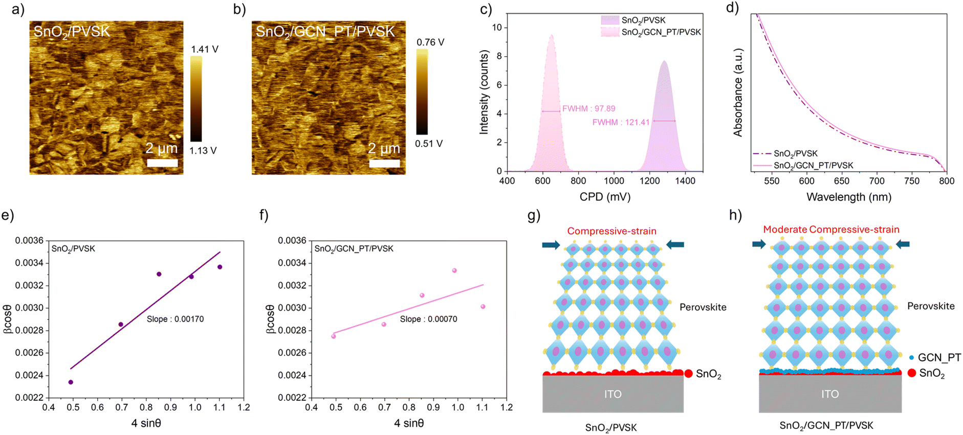 | ||
| Fig. 4 (a and b) CPD images acquired by KPFM for SnO2/PVSK and SnO2/GCN_PT/PVSK, respectively. (c) CPD distributions of SnO2/PVSK and SnO2/GCN_PT/PVSK samples. (d) Absorbance spectra. (e and f) W–H plots of SnO2/PVSK and SnO2/GCN_PT/PVSK samples. (g and h) Schematics depicting the changes in compressive strain in the perovskite layer with and without the GCN_PT layer. | ||
In addition to improved uniformity in CPD, Fig. 4d shows that the PVSK film on SnO2/GCN_PT exhibits slightly higher absorbance between 550 nm and 800 nm, the critical wavelength range for charge generation in PVSK absorbers. This enhanced light absorption can be attributed to the improved structural quality and reduced defect density conferred by the GCN_PT interfacial layer. We believe that GCN_PT facilitates a homogeneous deposition onto SnO2, resulting in a more conformal and electronically uniform surface, as observed in Fig. S5.† This uniformity appears to reduce the energy required for nucleation and growth during perovskite crystallization, enhancing overall crystallinity and light absorption. In addition, surface hydrophobicity also plays a crucial role in determining perovskite crystal structure and film quality. The SnO2/GCN_PT layer exhibits a significantly higher contact angle (48.25°) than SnO2 (27.84°), indicating a more hydrophobic surface as shown in Fig. S12.† Such difference in surface energy is one of the key factors contributing to the improved perovskite morphology and crystallinity.24 Based on this hypothesis, we evaluated the structural improvements in the PVSK layer by conducting XRD and Williamson–Hall (W–H) analyses. The complete XRD scans are provided in Fig. S13.† The W–H plot highlights a significant reduction in microstrain, an indicator of lattice distortion, in the SnO2/GCN_PT/PVSK sample compared to the SnO2/PVSK sample. Specifically, the SnO2/PVSK sample exhibits a microstrain value of 0.00170 (Fig. 4e), whereas the SnO2/GCN_PT/PVSK sample shows a markedly lower value of 0.00070 (Fig. 4f). Perovskite films inherently experience compressive strain due to factors such as thermal mismatch with the substrate, lattice contraction during crystallization, ion redistribution, and defect passivation.25Fig. 4g and h present schematic representations of the changes in compressive strain within the perovskite layer induced by incorporating the GCN_PT layer. The reduced oxygen vacancies at the SnO2 surface, combined with the conformal and uniform coating of the GCN_PT layer, effectively mitigate the strain in the perovskite layer.
We confirmed the effect of the GCN_PT layer on the PVSK layer and observed enhanced light absorption, a more homogeneous work function, and reduced microstrain stress in the perovskite film. To further investigate the impact of the GCN_PT layer, we evaluated the device performance of PSCs incorporating this layer. The perovskite compositions studied were FAPbI3 with a bandgap of 1.53 eV and Cs0.17FA0.83Pb(I0.6Br0.4)3 with a wide bandgap of 1.8 eV. The device architecture is shown in Fig. 5a, where the GCN_PT layer was inserted between the SnO2 ETL and the perovskite layer.
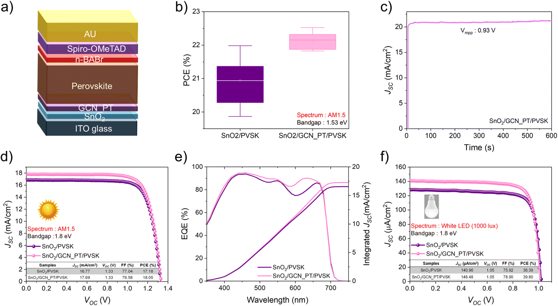 | ||
| Fig. 5 (a) Schematic representation of the structure of the perovskite solar cells. (b) Box plot of the PCE for FAPbI3-based perovskite solar cells under AM1.5 conditions. (c) SPO of the SnO2/GCN_PT/PVSK solar cell under continuous illumination. (d) J–V curves of wide-bandgap (1.8 eV) perovskite solar cells for SnO2/PVSK and SnO2/GCN_PT/PVSK under AM1.5 conditions. (e) EQE spectra of the wide-bandgap perovskite solar cells. (f) J–V curves of wide-bandgap perovskite solar cells under 1000 lux white LED illumination. | ||
To optimize the performance of the GCN_PT interfacial layer, we varied its thickness by controlling the spin-coating speed. The optimal deposition speed was determined to be 3000 rpm (Fig. S14†), which resulted in the highest improvement across all photovoltaic parameters compared to the SnO2 control sample. The approximate thickness of the GCN_PT layer on SnO2 was confirmed to be 1 nm based on the AFM line profile (Fig. S15†). As shown in Fig. 5b, the box plot of the PCE for FAPbI3-based devices. The SnO2/GCN_PT/PVSK devices achieved an average PCE of 22.13%, which is higher than the 20.95% observed for SnO2/PVSK devices. Box plots for other photovoltaic parameters are provided in Fig. S16.† Although the thickness of the perovskite layer is similar for both samples (around 564 nm), as shown in Fig. S17,† the primary improvement came from the JSC, attributed to the enhanced conductivity of the GCN_PT layer after plasma modification and the improved light absorption of the PVSK layer. Furthermore, Fig. S18a and b† presents steady-state photoluminescence and time-resolved photoluminescence measurements, respectively. The SnO2/GCN_PT/PVSK film exhibits a lower PL peak intensity, and a shorter carrier lifetime compared to the SnO2/PVSK film. These findings confirm that the GCN_PT layer facilitates more efficient charge extraction at the interface, thereby reducing carrier recombination losses. Fig. S19a† highlights the enhancement in external quantum efficiency (EQE) between 750 and 800 nm, directly contributing to increased JSC. Fig. S19b† presents the internal quantum efficiency (IQE) data, demonstrating that the GCN_PT layer significantly improves charge extraction and reduces defect-related recombination, particularly at longer wavelengths, thereby enhancing the intrinsic efficiency of the perovskite solar cells. There is an average PCE and parameter of both samples, as shown in Table S1.† The stabilized power output (SPO) data in Fig. 5c shows that the JSC remained stable over 10 minutes of continuous illumination for SnO2/GCN_PT/PVSK devices, indicating efficient charge transport and minimal recombination under operational conditions. Moving to wide bandgap perovskites (1.8 eV), it also shows the improved JSC with GCN_PT layer.
In the case of wide bandgap perovskites, it inherently faces challenges such as VOC deficit26 and lower JSC, stemming from their limited light absorption range and increased susceptibility to carrier recombination. The larger bandgap results in a greater energy separation between the conduction and valence bands, exacerbating carrier trapping at recombination sites. Furthermore, the higher bromine (Br) content (40%) in the wide-bandgap composition introduces additional defects, as Br's greater reactivity compared to iodine often disrupts perovskite crystal growth due to its faster interaction with precursor components during crystallization.27
Interestingly, the application of the GCN_PT layer significantly improved the EQE in the 450–680 nm range, as shown in Fig. 5e. This enhancement likely arises from improved charge extraction and defect passivation at the interface, effectively benefiting the wide bandgap perovskite layer. The wide bandgap PSCs were tested under 1000 lux white LED lighting to explore its performance under low-light conditions. The GCN_PT layer notably enhanced the JSC (∼8 μA cm−2) compared to SnO2/PVSK devices, overcoming the typical limitations of low-light intensity. Consequently, the device incorporating the GCN_PT layer achieved an outstanding PCE of approximately 39.80% under 1000 lux indoor conditions.
Conclusion
Improving the charge extraction properties of PSCs are highly desirable for its use in indoor applications under limited light intensities. To enhance the charge extraction properties of PSCs for indoor applications, we demonstrate the effectiveness of plasma-modified GCN as an interfacial layer between SnO2 and perovskite layers in n-i-p structured perovskite solar cells. Low temperature, aqueous media assisted plasma modification process significantly modified the structural and electronic properties of GCN, enhancing its conductivity and improving its compatibility with SnO2. XPS and MD simulations revealed that the plasma-induced graphitization and nitrogen vacancies contributed to enhanced charge transport and defect passivation at the SnO2/GCN_PT interface. The perovskite films grown on SnO2/GCN_PT exhibited reduced microstrain, improved crystallinity, and more uniform work function distribution, as evidenced by KPFM and W–H analysis. The device performance tests revealed that the inclusion of the GCN_PT layer enhanced the JSC through improved interfacial charge extraction and reduced recombination, as well as increased light absorption in the longer wavelength range. Notably, wide-bandgap perovskite solar cells also benefited from the GCN_PT layer, showing significant improvements in JSC and PCE under both AM1.5 and indoor lighting conditions, achieving a PCE of approximately 39.80% under 1000 lux white LED light. These findings highlight the potential of plasma-modified GCN as a versatile interfacial layer to improve charge transport and defect passivation in perovskite solar cells, particularly in wide-bandgap and indoor photovoltaic applications. The proposed plasma modification strategy provides a scalable and effective pathway to enhance the functional properties of nanomaterials and improves the performance and stability of perovskite devices, paving the way for next-generation photovoltaics devices.Data availability
The data supporting this article have been included as part of the ESI.†Author contributions
M. L. conducted solar cell experiments and data curation & analysis and manuscript preparation, E. Y. M. A., W. T. and P. C. W. conducted molecular dynamics simulation and wrote parts of the manuscript, S. W. K., S. Y. L. conducted carbon nanomaterial synthesis & modifications and data curation & analysis. T. Y. N., M. A. G., contributed to analytical data curation and reviewing and editing of the manuscript. Conceptualization, supervision and writing—review and editing was conducted by X. H., J. S. Y. and D. H. S.Conflicts of interest
The authors declare no conflict of interest.Acknowledgements
D. H. S. acknowledges the support of the Korea Institute of Energy Technology Evaluation and Planning (KETEP) and the Ministry of Trade, Industry & Energy (MOTIE) of the Republic of Korea (No. 20224000000100). J. S. Y. acknowledges support from the Australian Research Council through Discovery Grants and the ARC Centre of Excellence in Future Low Energy Electronics Technologies (FLEET). The authors acknowledge the scientific and technical assistance of the Electron Microscope Unit and Solid State & Elemental Analysis Unit at the University of New South Wales (UNSW). The authors also acknowledge the support of TEM analysis at Korea Institute of Energy Technology (KENTECH) supported by Center for Shared Research Facilities.References
- Best research-cell efficiency chart, NREL, https://www.nrel.gov/pv/cell-efficiency.html.
- M. A. Green, A. Ho-Baillie and H. J. Snaith, Nat. Photonics, 2014, 8(7), 506 CrossRef CAS.
- N. J. Jeon, J. H. Noh, W. S. Yang, Y. C. Kim, S. Ryu, J. Seo and S. I. Seok, Nature, 2015, 517(7535), 476 CrossRef CAS PubMed.
- J. M. Howard, E. M. Tennyson, S. Barik, R. Szostak, E. Waks, M. F. Toney, A. F. Nogueira, B. R. A. Neves and M. S. Leite, J. Phys. Chem. Lett., 2018, 9(12), 3463 CrossRef CAS PubMed.
- F. Lehmann, A. Franz, D. M. Többens, S. Levcenco, T. Unold, A. Taubert and S. Schorr, RSC Adv., 2019, 9(20), 11151 RSC.
- M. Kim, G.-H. Kim, T. K. Lee, I. W. Choi, H. W. Choi, Y. Jo, Y. J. Yoon, J. W. Kim, J. Lee, D. Huh, H. Lee, S. K. Kwak, J. Y. Kim and D. S. Kim, Joule, 2019, 3(9), 2179 CrossRef CAS.
- J. Park, J. Kim, H.-S. Yun, M. J. Paik, E. Noh, H. J. Mun, M. G. Kim, T. J. Shin and S. I. Seok, Nature, 2023, 616(7958), 724 CrossRef CAS PubMed.
- J. W. Yoo, E. Noh, J. Jang, K. S. Lee, J. Byeon, M. Choi, J. Im and S. I. Seok, Joule, 2023, 7(4), 797 CrossRef CAS.
- J. Wang, H. Zhang, L. Wang, K. Yang, L. Cang, X. Liu and W. Huang, ACS Appl. Energy Mater., 2020, 3(5), 4484 CrossRef CAS.
- B. Shi, B. Liu, J. Luo, Y. Li, C. Zheng, X. Yao, L. Fan, J. Liang, Y. Ding, C. Wei, D. Zhang, Y. Zhao and X. Zhang, Sol. Energy Mater. Sol. Cells, 2017, 168, 214 CrossRef CAS.
- H. Zhou, Q. Chen, G. Li, S. Luo, T.-b. Song, H.-S. Duan, Z. Hong, J. You, Y. Liu and Y. Yang, Science, 2014, 345(6196), 542 CrossRef CAS PubMed.
- H. Li, B. Yu and H. Yu, Adv. Funct. Mater., 2024, 34(37), 2402128 CrossRef CAS.
- X. Wei, Y. Sun, Y. Zhang, B. Yu and H. Yu, Nano Energy, 2025, 133, 110513 CrossRef CAS.
- G. Wu, R. Liang, M. Ge, G. Sun, Y. Zhang and G. Xing, Adv. Mater., 2022, 34(8), 2105635 CrossRef CAS PubMed.
- B. Chen, H. Chen, Y. Hou, J. Xu, S. Teale, K. Bertens, H. Chen, A. Proppe, Q. Zhou, D. Yu, K. Xu, M. Vafaie, Y. Liu, Y. Dong, E. H. Jung, C. Zheng, T. Zhu, Z. Ning and E. H. Sargent, Adv. Mater., 2021, 33(41), 2103394 CrossRef CAS PubMed.
- M. Lee, J. Lim, E. Choi, A. M. Soufiani, S. Lee, F.-J. Ma, S. Lim, J. Seidel, D. H. Seo, J.-S. Park, W. Lee, J. Lim, R. F. Webster, J. Kim, D. Wang, M. A. Green, D. Kim, J. H. Noh, X. Hao and J. S. Yun, Adv. Mater., 2024, 36(41), 2402053 CrossRef CAS PubMed.
- C. Zhang, S. Wang, H. Zhang, Y. Feng, W. Tian, Y. Yan, J. Bian, Y. Wang, S. Jin, S. M. Zakeeruddin, M. Grätzel and Y. Shi, Energy Environ. Sci., 2019, 12(12), 3585 RSC.
- Z. Liu, S. Wu, X. Yang, Y. Zhou, J. Jin, J. Sun, L. Zhao and S. Wang, Nanoscale Adv., 2020, 2(11), 5396 RSC.
- N. H. Hemasiri, M. Ashraf, S. Kazim, R. Graf, R. Berger, N. Ullah, M. N. Tahir and S. Ahmad, Nano Energy, 2023, 109, 108326 CrossRef CAS.
- L. Wang, L. Fu, B. Li, H. Li, L. Pan, B. Chang and L. Yin, Sol. RRL, 2021, 5(3), 2000720 CrossRef CAS.
- C. E. Anderson, N. R. Cha, A. D. Lindsay, D. S. Clark and D. B. Graves, Plasma Chem. Plasma Process., 2016, 36, 1393 CrossRef CAS.
- R. Zhou, Y. Zhao, R. Zhou, T. Zhang, P. Cullen, Y. Zheng, L. Dai and K. Ostrikov, Carbon Energy, 2023, 5(1), e260 CrossRef.
- J. J. Yoo, G. Seo, M. R. Chua, T. G. Park, Y. Lu, F. Rotermund, Y.-K. Kim, C. S. Moon, N. J. Jeon, J.-P. Correa-Baena, V. Bulović, S. S. Shin, M. G. Bawendi and J. Seo, Nature, 2021, 590(7847), 587 CrossRef CAS PubMed.
- C. Bi, Q. Wang, Y. Shao, Y. Yuan, Z. Xiao and J. Huang, Nat. Commun., 2015, 6(1), 7747 CrossRef CAS PubMed.
- H. Min, S.-G. Ji and S. I. Seok, Joule, 2022, 6(9), 2175 CrossRef CAS.
- R. H. Ahangharnejhad, J. D. Friedl, A. B. Phillips and M. J. Heben, Sol. Energy Mater. Sol. Cells, 2021, 225, 111015 CrossRef CAS.
- T. Huang, S. Tan, S. Nuryyeva, I. Yavuz, F. Babbe, Y. Zhao, M. Abdelsamie, M. H. Weber, R. Wang, K. N. Houk, C. M. Sutter-Fella and Y. Yang, Sci. Adv., 2021, 7(46), eabj1799 CrossRef CAS PubMed.
Footnote |
| † Electronic supplementary information (ESI) available. See DOI: https://doi.org/10.1039/d5ta00480b |
| This journal is © The Royal Society of Chemistry 2025 |