Strain and U driven phase transitions in monolayer intrinsic ferrovalley NbIn2As2Se2†
Jiajun
Zhu
 a,
Heyun
Zhao
 a and
Wanbiao
Hu
 *abcd
*abcd
aYunnan Key Laboratory of Electromagnetic Materials and Devices, National Center for International Research on Photoelectric and Energy Materials, School of Materials and Energy, Yunnan University, Kunming 650091, P. R. China. E-mail: huwanbiao@ynu.edu.cn
bElectron Microscopy Center, Yunnan University, Kunming 650091, P. R. China
cSouthwest United Graduate School, Kunming 650092, P. R. China
dSchool of Engineering, Yunnan University, Kunming 650091, P. R. China
First published on 30th October 2024
Abstract
The manipulation of the valley degree of freedom presents opportunities for both research and practical application. In this work, we theoretically demonstrate that the intrinsic valley anomalous Hall effect can exist in monolayer NbIn2As2Se2. Due to time-reversal symmetry breaking, monolayer NbIn2As2Se2 is an out-of-plane magnetization semiconductor with a Curie temperature of 232 K. The ability to induce phase transitions in the material through strain and the U value leads to different electronic states like the valley quantum anomalous Hall effect and the half-valley-metal state. The chiral-spin-valley locking of edge states and the band inversion of the d orbital of Nb at the K/K′ valley offer insights into the mechanisms behind these transitions. These findings not only contribute to the fundamental understanding of topology, spintronics, and valleytronics, but also pave the way for potential practical applications and experimental investigations in this exciting and rapidly evolving field.
Valleys, as regulated information storage similar to charge and spin, have garnered significant interest in recent years due to their outstanding properties and promising prospects for applications in valleytronic devices.1–3 Valleytronic materials typically feature at least two valleys in momentum space, with these valleys representing either local minima or local maxima on the band structure.4,5 Typically, these two valleys possess degenerate energy and inequivalent Berry curvatures, located at the K and K′ points.6,7 Experimental observations have shown that optical pumping can induce valley polarization in transition metal dichalcogenides (TMDCs), which can be explained by valley-contrasting optical selection rules.8–10 Additional methods, such as manipulating magnetic fields, utilizing magnetic doping, and capitalizing on the magnetic proximity effect, can provide alternative pathways to achieve and sustain valley polarization.11–13 Nevertheless, the magnetic field exhibits low efficiency (0.1–0.2 meV T−1), magnetic doping tends to elevate impurity scatterings across distinct valleys, and a magnetic substrate obscures the valley physics within the host materials.14–16 Hence, the quest for intrinsic valley polarization is crucial.
Furthermore, the progress in valleytronic materials has led to a new insight into 2D ferromagnetic (FM) systems, known as ferrovalley materials.17–19 FM semiconductors inherently break the time-reversal symmetry, and when coupled with spin–orbit coupling (SOC), they exhibit spontaneous valley polarization phenomena.20 The quantum anomalous valley Hall effect (QAVHE) is easily observed experimentally in ferrovalley materials, making them have great application potential in information storage.21 Achieving spontaneous valley polarization requires out-of-plane magnetism, whereas in-plane magnetic materials are more commonly found in nature.22–24 Therefore, a difficult-to-modulate magnetic axis is necessary for realizing spontaneous valley polarization.25,26 To date, several ferrovalley materials have been theoretically predicted, including VSi2P4, VSiGeN4, NbX2, Fe2SSe, Nb3I8, 2H-VSe2, and GdI2.6,27–30 On the other hand, valleys combined with other physical properties can give rise to new physical phenomena, such as the valley quantum anomalous Hall effect (VQAHE), which emerges from the coupling between valley polarization and topology insulators (TI).31,32 Despite their high value, materials that combine the quantum anomalous Hall effect (QAHE) and the VQAHE are exceedingly rare. Consequently, the design of multi-functional multi-valley materials holds great significance in materials science and condensed matter physics.
Recently, a two-dimensional van der Waals material, MoSi2N4, with seven atomic layers, was experimentally synthesized using the chemical vapor deposition (CVD) method.33 The monolayer MoSi2N4 can be viewed as composed of monolayer 2H-MoS2-like structure MoN2 and bilayer silicene-like structure SiN, exhibiting K valley polarization phenomena similar to 2H-MoS2.34 Spontaneous valley polarization can be achieved by introducing magnetism to break the time-reversal symmetry. Here, we theoretically predict a 2D FM material, NbIn2As2Se2, with a structure similar to MoSi2N4. Based on first-principles, the monolayer NbIn2As2Se2 is a semiconductor with out-of-plane FM at U = 3 eV and has a Curie temperature (TMC) of 232 K. We also confirm that the VQAHE can be observed in this material. The material can achieve phase transition by applying in-plane biaxial strain engineering or adjusting the value of U. These findings indicate that monolayer intrinsic ferrovalley NbIn2As2Se2 holds promise for applications in spintronics and valleytronics.
This work was performed as implemented in the Vienna ab initio simulation package, which was based on density functional theory.35,36 The exchange–correlation interaction between electrons was described by the Perdew–Burke–Ernzerhof (PBE) type generalized gradient approximation (GGA).37 The energy cutoff of 500 eV and 13 × 13 × 1 k-meshes for Brillouin-zone (BZ) sampling were chosen. The calculation results of the convergence criterion for force and energy were selected as 10−3 eV Å−1 for and 10−6 eV. Due to the strong correlation effect, we use the GGA+U method in the 3d orbital of Nb element.38
To verify the stability of the material, calculations of the phonon dispersions of monolayer NbIn2As2Se2 were performed based on density functional perturbation theory (DFPT) by using the PHONOPY code. The molecular dynamics simulation based on the NVT ensemble was conducted to demonstrate the thermal stability by using the Nosé–Hoover method at 300 K. A 5 × 5 × 1 supercell and a 3 × 3 × 1 Monkhorst–Pack grid were employed in phonon dispersions and MD simulations.
The FM Curie temperature was determined through Monte Carlo (MC) simulations using a 30 × 30 × 1 supercell and 108 loops with the Mcsolve code.39 The Fukui method was employed in the Berry curvature calculation using the VASPBERRY code.40,41 We calculated the valley Hall effect through the use of the WANNIER90 and WANNIERTOOLS packages.42,43
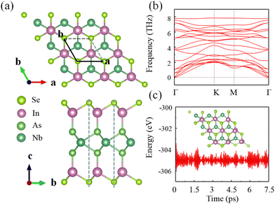
Fig. 1(a) shows the side and the top view of monolayer NbIn2As2Se2, which consists of Se–In–As–Nb–As–In–Se seven atom layers in a unit cell. The monolayer NbIn2As2Se2 structure can be viewed as consisting of three parts, in which the upper/lower part is a β-P-like structure InSe layer, the middle part NbAs2 shares the same crystal structure with 2H-MoS2, and the upper/lower middle layers are connected by In–As binding. It possesses a 2D hexagonal lattice which has P6m2 symmetry with space group no. 187. The monolayer NbIn2As2Se2 structure maintains the Mz symmetry about the Nb atom, which can lead to many novel properties, such as hidden physics. We consider the influence of the U value on lattice constant a, optimizing the lattice constants a for different U values, shown in Fig. S1(a) (ESI†). It can be found that the lattice constant a increases with the increase of the U value, from 3.918 Å to 3.950 Å.
To estimate the stability of monolayer NbIn2As2Se2, the formation energy Eform and the cohesive energy Ecoh were calculated through the equations: Eform = (ENbIAS − μNb − 2μIn − 2μAs − 2μSe)/7 and Ecoh = (ENbIAS − ENb − 2EIn − 2EAs − 2ESe)/7, where ENbIAS, μNb/In/As/Se and ENb/In/As/Se are the total energy of monolayer NbIn2As2Se2 and the energy of Nb, In, As and Se atoms in a stable bulk phase structure or isolated state. The calculated values of Eform and Ecoh are −0.23 eV and −4.51 eV per atom for monolayer NbIn2As2Se2. The negative value of Eform indicates that monolayer NbIn2As2Se2 can be synthesized from the pure phase Nb, In, As, and Se elements. Our Ecoh is lower than the Ecoh values of some theoretically predicted two-dimensional materials, such as Cu2Ge (−3.17 eV per atom)44 and CeI2 (−3.14 eV per atom),6 indicating that the monolayer NbIn2As2Se2 is stable.
To evaluate the thermodynamic stability of monolayer NbIn2As2Se2, the phonon dispersion calculations and molecular dynamics simulations have been performed. Phonon dispersion can describe the dynamic stability of a material, which needs all phonons across the whole Brillouin zone. Fig. 1(b) clearly displays that there is no virtual frequency in the Brillouin zone at U = 3 eV, confirming the dynamic stability of monolayer NbIn2As2Se2. The MD simulation can evaluate the thermal stability of monolayer NbIn2As2Se2. Fig. 1(c) demonstrates that the structure remains stable for at least 7.5 ps at a temperature of 300 K. The Born–Huang criteria can be used to evaluate the mechanical stability,45 which requires C11C22 > C122 and C66 > 0 for a 2D hexagonal lattice. The value of the elastic constant is about C11 = 109.5 N m−1, C12 = 44.5 N m−1 and C66 = 38.7 N m−1 at U = 3 eV. We checked these values for the Born–Huang criterion and confirmed monolayer NbIn2As2Se2 is mechanically stable.
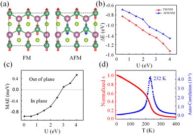
In order to define the magnetic ground state of monolayer NbIn2As2Se2, we constructed a magnetic configuration by using a 2 × 2 rectangular supercell in Fig. 2(a). The ground state of the system can be represented by the total energy difference (ΔE) between FM/antiferromagnetic (AFM) and nonmagnetic (NM) states and a graph of ΔE–U is plotted in Fig. 2(b), demonstrating that the system is in the FM state at different U values. Spontaneous valley polarization requires an out-of-plane magnetic direction, so it is crucial to understand the magnetic orientation of the system. Here, we plotted the MAE at different U values in Fig. 2(c), which can be calculated as EMAE = E100 − E001 within GGA+SOC+U. The MAE can determine magnetic anisotropy, where a positive value indicates out-of-plane magnetism as the ground state, while a negative value indicates in-plane magnetism as the ground state. In the range of U = 0–3 eV, in-plane magnetism is the ground state. As the U value increases (U ≥ 3), the magnetic direction changes from in-plane to out-of-plane. Therefore, in the following discussion, our calculation results are primarily obtained under the condition of U = 3 eV. The magnetic moment is a crucial parameter in a ferromagnetic system, with the magnetism primarily originating from the Nb atom in our materials. Hence, we employed two methods, namely the electron localization function (ELF) and Bader charge, to analyze the environment surrounding the Nb atom. Fig. S1(b) (ESI†) illustrates the ELF in the (110) plane of monolayer NbIn2As2Se2. The Nb atom has a lower electron density, in contrast to the Se atom which has a higher electron density, indicative of an ionic bond between Nb and Se atoms, implying a transfer of charge from Nb to Se. Through Bader charge analysis, it was verified that Nb atoms transferred 0.6 electrons to each Se atom. Consequently, the calculation results indicate a magnetic moment per Nb of 1μB at U = 3 eV.
T MC is an important parameter in magnetic materials, which can be estimated using the Heisenberg model:
 | (1) |
| EFM = E0 − 6JS2 | (2) |
| EAFM = E0 + 2JS2 | (3) |
 | (4) |
The calculated normalized J is 74.9 meV at U = 3 eV, and the normalized magnetic moment and auto-correlation vs. temperature are plotted in Fig. 2(d). The predicted TMC is 232 K. On the other hand, the transition temperature can be expressed as  by using the mean-field approximation (MFA), where J and KB are the nearest-neighboring exchange parameter and Boltzmann constant, respectively. The value of TMFC is 579 K, which is higher than TMC (232 K). Fig. S2 (ESI†) shows the TMC of NbIn2As2Se2 at different values of U and the result that the TMC decreases as the U value increases.
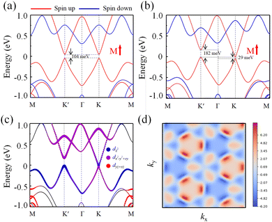
Fig. 3(a) shows the spin polarized band structure of monolayer NbIn2As2Se2 without the SOC effect. It can be seen that both the conduction band (CB) and the valence band (VB) near the Fermi level come from the spin-up channel for M↑. When the magnetic direction changes to M↓, as shown in Fig. S4 (ESI†), the CB and VB come from the spin-down channel, which is in contrast to the result when the magnetic direction is M↑. Theoretical calculations reveal that the conduction band minimum (CBM) and valence band maximum (VBM) both reside at the K or K′ point, with a band gap value of 104 meV, indicating that monolayer NbIn2As2Se2 is a FM semiconductor. When the inversion symmetry is broken, the two K valleys will no longer be equal. Under the effect of the SOC, bands at the K and K′ points experience a shift, resulting in spontaneous valley polarization. The calculated band gap value is 29 meV at the K point, which is lower than the band gap of 182 meV at the K′ point, as depicted in Fig. 3(b). As shown in Fig. S3 (ESI†), external magnetic fields can be used to control band gap. When the magnetic direction becomes M(↓), both the VB and CB near the Fermi surface come from the spin-down channel, and the band gap values at K and K′ points are exchanged.
The above results confirm that the monolayer NbIn2As2Se2 is a FM semiconductor with an out-of-plane magnetic orientation. In the presence of SOC, it can spontaneously generate valley polarization. As is well-known, the SOC effects can be written as
Ĥsoc = α![[L with combining circumflex]](https://www.rsc.org/images/entities/i_char_004c_0302.gif) z z | (5) |
![[L with combining circumflex]](https://www.rsc.org/images/entities/i_char_004c_0302.gif) z is the orbital angular momentum along the c direction. The orbital projection of Nb atoms near the Fermi level is shown in Fig. 3(c). At the K point, the VBM is mainly contributed by the dx2−y2 + dxy orbital, while the CBM is almost entirely the dz2 orbital. Unlike the orbital projection at the K valley, the orbital contributions of the Nb atoms at the K′ point are opposite to those at the K point. Therefore, it can be considered that the different valley polarization at the K and K′ points originates from their different orbital contributions near the Fermi level. Since the magnetic quantum number for dz2 is 0, the basis functions at K and K′ points can be represented by dx2−y2 and dxy orbitals. Considering the presence of C3h symmetry operations in the system, the basis functions can be written as
z is the orbital angular momentum along the c direction. The orbital projection of Nb atoms near the Fermi level is shown in Fig. 3(c). At the K point, the VBM is mainly contributed by the dx2−y2 + dxy orbital, while the CBM is almost entirely the dz2 orbital. Unlike the orbital projection at the K valley, the orbital contributions of the Nb atoms at the K′ point are opposite to those at the K point. Therefore, it can be considered that the different valley polarization at the K and K′ points originates from their different orbital contributions near the Fermi level. Since the magnetic quantum number for dz2 is 0, the basis functions at K and K′ points can be represented by dx2−y2 and dxy orbitals. Considering the presence of C3h symmetry operations in the system, the basis functions can be written as | (6) |
| Eτ = 〈ϕτ|Ĥsoc|ϕτ〉 | (7) |
Therefore, due to the SOC effect, the dx2−y2 and dxy orbitals near the Fermi level shift, resulting in different energy eigenvalues and leading to spontaneous valley polarization, which can be expressed as
 | (8) |
The above equation helps us understand that valley polarization arises from the SOC effect causing the degenerate K/K′ valleys to shift, resulting in the two valleys no longer being equivalent.
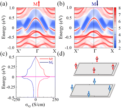
In 2D materials, the Chern number C can be used to characterize the quantum anomalous Hall effect, which can be expressed as46,47
 | (9) |
 | (10) |
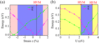
In order to understand the relationship between strain and electronic structure, we apply biaxial in-plane strain in the system monolayer NbIn2As2Se2 and plot the band gap at the K or K′ valley as a function of strain ε in Fig. 5(a). Under the influence of strain, it can be observed that the system undergoes a transition from a half-metal to a TI to a half-metal. Notice that the systems transform into a half-valley-material (HVM) state at ε = 0.5%. This state means that one valley is a semiconductor and the other is a metal. When strain ε > 1.4%, the value of band gap at the K or K′ valley increases and few electrons occupy the CB at the K valley, and the systems become half-metal. Akin to tensile strain, as compressive strain increases, the system transitions to a half-metal state at ε = −2%. Until the strain is greater than −2%, few electrons occupy the VB at the K′ valley, and the systems become half-metal. As shown in Fig. S4 (ESI†), the dz2 and dx2−y2 at K and K′ have a competitive relationship via strain engineering. The inversion of the dz2 and dx2−y2 orbitals occurs at the valleys at the K or K′ point after a process of closing and reopening. This process can be explained by the deformation of Nb atoms under strain. Tensile strain reduces the overlap between the dz2 orbital of Nb and the pz orbital of Se, while compressive strain increases the overlap between the dz2 orbital of Nb and the pz orbital of Se, resulting in a decrease in energy during tension and an increase in energy during compression.
We have also considered the influence of the U value on the band gap at the K or K′ valley, plotted in Fig. 5(b). It clearly demonstrates that monolayer NbIn2As2Se2 is in the ferrovalley phase for U = 0.0–2.2 or 3.4–4.0 eV and in the TI phase for U = 2.2–3.4 eV, and the corresponding topological edge states are shown in Fig. S6 (ESI†). On the other hand, the U value can also regulate the band gap value at the K or K′ valley. As the U value increases, the band gap at the K or K′ valley will undergo a process of opening–closing–opening state. Similar to strain engineering, when U = 2.2 or 3.4 eV, the band gap at the K or K′ point closes, and monolayer NbIn2As2Se2 exhibits HVM behavior. We have also observed that the system transitions from the TI state to a ferrovalley state after passing through the HVM state, which is akin to strain effects. The results above demonstrate two methods to manipulate the performance of monolayer NbIn2As2Se2, thereby enhancing its potential applications in spintronic devices.
In summary, monolayer NbIn2As2Se2 is confirmed to be a ferrovalley material with TI via first-principles calculations. We discussed the structural stability in terms of energy, phonon dispersion, molecular dynamics, and mechanical properties. The FM state is the ground state for monolayer NbIn2As2Se2 with a TMC of 232 K at U = 3 eV, and the MAE confirms the out-of-plane magnetization direction, thus inducing spontaneous valley polarization. As the system exhibits the VQAHE, reversing the magnetic direction allows for the observation of chiral spin-valley edge states. Strain engineering and the U value can control the state of the system, such as the half-metal, TI and ferrovalley states. Our work provides theoretical guidance for exploring interactions among the FM, valleys, and TI, and offers candidate materials for valleytronic devices.
Data availability
The data that support the findings of this study are available with the corresponding author and can be obtained upon reasonable request.Conflicts of interest
There are no conflicts to declare.Acknowledgements
This work was supported by the Natural Science Foundation of China (Grant No. 22175150 and U2002217). We thank Dr Botao Fu for valuable discussion.References
- O. Gunawan, Y. P. Shkolnikov, K. Vakili, T. Gokmen, E. P. De Poortere and M. Shayegan, Valley Susceptibility of an Interacting Two-Dimensional Electron System, Phys. Rev. Lett., 2006, 97, 186404 CrossRef CAS PubMed.
- D. Xiao, W. Yao and Q. Niu, Valley-Contrasting Physics in Graphene: Magnetic Moment and Topological Transport, Phys. Rev. Lett., 2007, 99, 236809 CrossRef PubMed.
- J. R. Schaibley, H. Yu, G. Clark, P. Rivera, J. S. Ross, K. L. Seyler, W. Yao and X. Xu, Valleytronics in 2D materials, Nat. Rev. Mater., 2016, 1, 1 Search PubMed.
- H. Chen, R. Liu, J. Lu, X. Zhao, G. Hu, J. Ren and X. Yuan, Intrinsic valley-polarized quantum anomalous Hall effect and controllable topological phase transition in Janus Fe2SSe, J. Phys. Chem. Lett., 2022, 13, 10297 CrossRef CAS PubMed.
- A. Kormányos, V. Zólyomi, V. I. Fal’ko and G. Burkard, Tunable Berry curvature and valley and spin Hall effect in bilayer MoS2, Phys. Rev. B, 2018, 98, 035408 CrossRef.
- K. Sheng, Q. Chen, H.-K. Yuan and Z.-Y. Wang, Monolayer CeI2: An intrinsic room-temperature ferrovalley semiconductor, Phys. Rev. B, 2022, 105, 075304 CrossRef CAS.
- A. Zhang, K. Yang, Y. Zhang, A. Pan and M. Chen, Electrically switchable valley polarization, spin/valley filter, and valve effects in transition-metal dichalcogenide monolayers interfaced with two-dimensional ferromagnetic semiconductors, Phys. Rev. B, 2021, 104, L201403 CrossRef CAS.
- K. F. Mak, K. He, J. Shan and T. F. Heinz, Control of valley polarization in monolayer MoS2 by optical helicity, Nat. Nanotechnol., 2012, 7, 494 CrossRef CAS PubMed.
- P. Rivera, K. L. Seyler, H. Yu, J. R. Schaibley, J. Yan, D. G. Mandrus, W. Yao and X. Xu, Valley-polarized exciton dynamics in a 2D semiconductor heterostructure, Science, 2016, 351, 688 CrossRef CAS.
- L. Li, L. Shao, X. Liu, A. Gao, H. Wang, B. Zheng, G. Hou, K. Shehzad, L. Yu and F. Miao, et al., Roomtemperature valleytronic transistor, Nat. Nanotechnol., 2020, 15, 743 CrossRef CAS PubMed.
- L. Xu, M. Yang, L. Shen, J. Zhou, T. Zhu and Y. P. Feng, Large valley splitting in monolayer WS2 by proximity coupling to an insulating antiferromagnetic substrate, Phys. Rev. B, 2018, 97, 041405 CrossRef CAS.
- T. Norden, C. Zhao, P. Zhang, R. Sabirianov, A. Petrou and H. Zeng, Giant valley splitting in monolayer WS2 by magnetic proximity effect, Nat. Commun., 2019, 10, 4163 CrossRef.
- J. Qi, X. Li, Q. Niu and J. Feng, Giant and tunable valley degeneracy splitting in MoTe2, Phys. Rev. B: Condens. Matter Mater. Phys., 2015, 92, 121403 CrossRef.
- D. MacNeill, C. Heikes, K. F. Mak, Z. Anderson, A. Kormányos, V. Zólyomi, J. Park and D. C. Ralph, Breaking of Valley Degeneracy by Magnetic Field in Monolayer MoSe2, Phys. Rev. Lett., 2015, 114, 037401 CrossRef CAS.
- G. Aivazian, Z. Gong, A. M. Jones, R.-L. Chu, J. Yan, D. G. Mandrus, C. Zhang, D. Cobden, W. Yao and X. Xu, Magnetic control of valley pseudospin in monolayer WSe2, Nat. Phys., 2015, 11, 148 Search PubMed.
- X.-X. Zhang, T. Cao, Z. Lu, Y.-C. Lin, F. Zhang, Y. Wang, Z. Li, J. C. Hone, J. A. Robinson and D. Smirnov, et al., Magnetic brightening and control of dark excitons in monolayer WSe2, Nat. Nanotechnol., 2017, 12, 883 CrossRef CAS.
- Q. Cui, Y. Zhu, J. Liang, P. Cui and H. Yang, Spinvalley coupling in a two-dimensional VSi2N4 monolayer, Phys. Rev. B, 2021, 103, 085421 CrossRef CAS.
- F. Withers, O. Del Pozo-Zamudio, A. Mishchenko, A. P. Rooney, A. Gholinia, K. Watanabe, T. Taniguchi, S. J. Haigh, A. Geim and A. Tartakovskii, et al., Light-emitting diodes by band-structure engineering in van der Waals heterostructures, Nat. Mater., 2015, 14, 301 CrossRef CAS PubMed.
- Z. He, R. Peng, X. Feng, X. Xu, Y. Dai, B. Huang and Y. Ma, Two-dimensional valleytronic semiconductor with spontaneous spin and valley polarization in single-layer Cr2Se3, Phys. Rev. B, 2021, 104, 075105 CrossRef CAS.
- R. Peng, Z. He, Q. Wu, Y. Dai, B. Huang and Y. Ma, Spontaneous valley polarization in two-dimensional organometallic lattices, Phys. Rev. B, 2021, 104, 174411 CrossRef CAS.
- Y. Chen, X. Zhao and Y. An, Prediction for an intrinsic ferrovalley semiconductor in a Janus 2H-CeBrCl monolayer with a high Curie temperature and perpendicular magnetic anisotropy, Phys. Rev. B, 2024, 109, 125421 CrossRef CAS.
- S.-D. Guo, J.-X. Zhu, W.-Q. Mu and B.-G. Liu, Possible way to achieve anomalous valley Hall effect by piezoelectric effect in a GdCl2 monolayer, Phys. Rev. B, 2021, 04, 224428 CrossRef.
- X. Wang, L. Liu, N. Wang, Y. Chen, T. Song, Z. Liu and X. Cui, First-Principles Study on Valley Polarization of Ferromagnetic PrBr2 Monolayer under Strain, J. Phys. Chem. C, 2024, 128, 6897 CrossRef CAS.
- Y. Tian, C.-B. Wang, B.-Y. Zhang, X. Kong and W.-J. Gong, Quantum layer spin Hall effect in sliding antiferromagnetic bilayers, J. Mater. Chem. C, 2024 10.1039/d4tc01255k.
- X. Li, J. Li, Z. Gao, Z. Niu, X. Bi, J. Gao, T. Cao and X. Fan, Reversible nonvolatile control of the anomalous valley Hall effect in two-dimensional multiferroic materials based on GdGe2, J. Mater. Chem. C, 2024, 12, 5451 RSC.
- C. Lei, S. Cao, Z. Gong, X. Li, Y. Ma, J. Gao, J. Bi, R. Ahuja and Z. Qian, Controllable dual-polarization valley physics in the strain-engineered 2D monolayer of VC2N4, J. Mater. Chem. C, 2024, 12, 2156 RSC.
- X. Feng, X. Xu, Z. He, R. Peng, Y. Dai, B. Huang and Y. Ma, Valley-related multiple Hall effect in monolayer VSi2P4, Phys. Rev. B, 2021, 104, 075421 CrossRef CAS.
- R. Peng, Y. Ma, X. Xu, Z. He, B. Huang and Y. Dai, Intrinsic anomalous valley Hall effect in single-layer Nb3I8, Phys. Rev. B, 2020, 102, 035412 CrossRef CAS.
- J. Liu, W.-J. Hou, C. Cheng, H.-X. Fu, J.-T. Sun and S. Meng, Intrinsic valley polarization of magnetic VSe2 monolayers, J. Phys.: Condens. Matter, 2017, 29, 255501 CrossRef.
- P. Liu, S. Liu, M. Jia, H. Yin, G. Zhang, F. Ren, B. Wang and C. Liu, Strain-driven valley states and phase transitions in Janus VSiGeN4 monolayer, Appl. Phys. Lett., 2022, 121, 063103 CrossRef CAS.
- F. Xue, J. Li, Y. Liu, R. Wu, Y. Xu and W. Duan, Valley-dependent multiple quantum states and topological transitions in germanene-based ferromagnetic van der Waals heterostructures, Phys. Rev. B, 2024, 109, 195147 CrossRef CAS.
- S.-D. Guo, W. Xu, Y. Xue, G. Zhu and Y. S. Ang, Layer-locked anomalous valley Hall effect in a twodimensional A-type tetragonal antiferromagnetic insulator, Phys. Rev. B, 2024, 109, 134426 CrossRef CAS.
- Y.-L. Hong, Z. Liu, L. Wang, T. Zhou, W. Ma, C. Xu, S. Feng, L. Chen, M.-L. Chen and D.-M. Sun, et al., Chemical vapor deposition of layered two-dimensional MoSi2N4 materials, Science, 2020, 369, 670 CrossRef CAS PubMed.
- C. Yang, Z. Song, X. Sun and J. Lu, Valley pseudospin in monolayer MoSi2N4 and MoSi2As4, Phys. Rev. B, 2021, 103, 035308 CrossRef CAS.
- P. E. Blöchl, Projector augmented-wave method, Phys. Rev. B: Condens. Matter Mater. Phys., 1994, 50, 17953 CrossRef.
- G. Kresse and J. Furthmüller, Efficient iterative schemes for ab initio total-energy calculations using a plane-wave basis set, Phys. Rev. B: Condens. Matter Mater. Phys., 1996, 54, 11169 CrossRef CAS PubMed.
- J. P. Perdew, K. Burke and M. Ernzerhof, Generalized Gradient Approximation Made Simple, Phys. Rev. Lett., 1996, 77, 3865 CrossRef CAS PubMed.
- I. V. Solovyev, P. H. Dederichs and V. I. Anisimov, Corrected atomic limit in the local-density approximation and the electronic structure of d impurities in Rb, Phys. Rev. B: Condens. Matter Mater. Phys., 1994, 50, 16861 CrossRef CAS.
- L. Liu, X. Ren, J. Xie, B. Cheng, W. Liu, T. An, H. Qin and J. Hu, Magnetic switches via electric field in BN nanoribbons, Appl. Surf. Sci., 2019, 480, 300 CrossRef CAS.
- H.-J. Kim, C. Li, J. Feng, J.-H. Cho and Z. Zhang, Competing magnetic orderings and tunable topological states in two-dimensional hexagonal organometallic lattices, Phys. Rev. B, 2016, 93, 041404 CrossRef.
- T. Fukui, Y. Hatsugai and H. Suzuki, Chern numbers in discretized Brillouin zone:efficient method of computing (spin) Hall conductances, J. Phys. Soc. Jpn., 2005, 74, 1674 CrossRef CAS.
- G. Pizzi, V. Vitale, R. Arita, S. Blüugel, F. Freimuth, G. Géranton, M. Gibertini, D. Gresch, C. Johnson and T. Koretsune, et al., Wannier90 as a community code: new features and applications, J. Phys.: Condens. Matter, 2020, 32, 165902 CrossRef CAS.
- Q. Wu, S. Zhang, H.-F. Song, M. Troyer and A. A. Soluyanov, WannierTools: An open-source software package for novel topological materials, Comput. Phys. Commun., 2018, 224, 405 CrossRef CAS.
- L.-M. Yang, I. A. Popov, A. I. Boldyrev, T. Heine, T. Frauenheim and E. Ganz, Post-anti-van’t Hoff-Le Bel motif in atomically thin germanium–copper alloy film, Phys. Chem. Chem. Phys., 2015, 17, 17545 RSC.
- Z.-J. Wu, E.-J. Zhao, H.-P. Xiang, X.-F. Hao, X.-J. Liu and J. Meng, Crystal structures and elastic properties of superhard IrN2 and IrN3 from first principles, Phys. Rev. B: Condens. Matter Mater. Phys., 2007, 76, 054115 CrossRef.
- D. J. Thouless, M. Kohmoto, M. P. Nightingale and M. den Nijs, Quantized Hall Conductance in a Two-Dimensional Periodic Potential, Phys. Rev. Lett., 1982, 49, 405 CrossRef CAS.
- D. Xiao, M.-C. Chang and Q. Niu, Berry phase effects on electronic properties, Rev. Mod. Phys., 2010, 82, 1959 CrossRef CAS.
- M.-C. Chang and Q. Niu, Berry phase, hyperorbits, and the Hofstadter spectrum: Semiclassical dynamics in magnetic Bloch bands, Phys. Rev. B: Condens. Matter Mater. Phys., 1996, 53, 7010 CrossRef CAS PubMed.
- Y. Yao, L. Kleinman, A. H. MacDonald, J. Sinova, T. Jungwirth, D.-S. Wang, E. Wang and Q. Niu, First Principles Calculation of Anomalous Hall Conductivity in Ferromagnetic bcc Fe, Phys. Rev. Lett., 2004, 92, 037204 CrossRef PubMed.
Footnote |
| † Electronic supplementary information (ESI) available. See DOI: https://doi.org/10.1039/d4tc03637a |
| This journal is © The Royal Society of Chemistry 2025 |

