Study on the time-resolved detection performance of β-Ga2O3-based SBUV photodetectors: surface chemical analysis and the impacts of non-VO factors†
Received
29th August 2024
, Accepted 3rd November 2024
First published on 8th November 2024
Abstract
The time-resolved detection performance of β-gallium oxide (β-Ga2O3)-based solar-blind ultraviolet (SBUV) photodetectors (PDs) are garnering extensive research attention. Generally, variations in the response and recovery rates of β-Ga2O3-based PDs have been attributed to oxygen vacancies (VO), typically analyzed through X-ray photoelectron spectroscopy (XPS) O 1s spectra. However, in this study, we fabricated SBUV PDs with β-Ga2O3 films grown via metal–organic chemical vapor deposition (MOCVD). The surface chemical analysis of the obtained films reveals that the XPS O 1s spectra are unaffected by VO. Additionally, by correlating film properties with PD performance, we demonstrate the significant role of non-VO factors in shaping the time-resolved detection performance of these devices.
Introduction
SBUV, ranging from 200 to 280 nm, is notably devoid of background noise, making it exceptionally valuable for the detection of missiles, the prevention of fires, and the monitoring of ozone layer depletion.1 β-Ga2O3 is celebrated for its intrinsic solar-blindness, outstanding thermal and chemical stability.2,3 Moreover, the large-scale production of β-Ga2O3 crystals is feasible through both melt growth and epitaxy techniques,4,5 which further cements its position as a material of choice for SBUV detection over other contenders such as ZnxMg1−xO, AlxGa1−xN, and diamond.6 Besides, β-Ga2O3 holds immense promise for applications in high-power devices and gas sensing technologies.7,8
The quintessential PDs should embody high sensitivity, high signal-to-noise ratio, high spectral selectivity, high speed, and remarkable stability.9 However, the intrinsic persistent photoconductivity (PPC) of β-Ga2O3 poses a challenge to achieving the high-speed demands. In recent years, a surge of literature has focused on the time-resolved detection performance of β-Ga2O3-based PDs. Notably, Vu et al. have shown that enhancing the oxygen partial pressure during pulsed laser deposition processes can mitigate the PPC of β-Ga2O3-based PDs,10 Wang et al. dissected the impact of post-annealing on the response and recovery speeds of β-Ga2O3-based PDs,11 while Deng et al. illustrated that surface plasma treatment can reduce the PPC of β-Ga2O3-based PDs.12 Furthermore, the works of Chen and Li et al. have brought to light the potential of PPC in β-Ga2O3 for applications in brain-like artificial intelligence fields.13,14 Collectively, current research predominantly attributes variations in time-resolved detection performance to oxygen vacancies (VO).10–13,15–19 The elongation of response and recovery times, ascribed to VO, is a trait shared by many oxide materials like tin dioxide and zinc oxide.20–22 Compared to its oxide counterparts, β-Ga2O3 exhibits unique features, such as its ultra-wide indirect bandgap, suggesting more intricate mechanisms at play in its time-resolved response characteristics.2 Additionally, XPS O 1s spectra are widely regarded as a key method for characterizing VO, yet the interpretations of O 1s spectra remain a contentious issue to date.23–26
In this paper, we fabricated SBUV PDs using β-Ga2O3 films grown by MOCVD. By fine-tuning the growth parameters of the β-Ga2O3 thin films, we delve into the influence of non-VO factors on the time-resolved detection performance of the PDs and explore the correlation between the XPS O 1s spectra and VO.
Experimental
Epitaxial growth
To meticulously analyze the relationship between the XPS O 1s spectra and VO, the O/Ga flow ratio (VI/III ratio) was selected as the variable of interest. The epitaxial growth was conducted using a modified Emcore D180 MOCVD system, with 2-inch c-plane sapphire wafers as substrates. High-purity oxygen (O2) and trimethylgallium (TMGa) served as the reactants. TMGa was transported by high-purity argon (Ar) through a bubbling method, with the pressure and temperature inside the bubbler maintained at 1200 mbar and 1 °C, respectively. The substrate temperature and growth pressure were controlled at 750 °C and 40 mbar, with the growth process lasting for a duration of 0.5 h. The flux of the reactants and the corresponding VI/III ratios are detailed in Table 1. The calculation of the VI/III ratios is based on the following equations:| | | nGa = FAr × PMO/[Vm × (Pbub − PMO)] | (2) |
where PMO denotes the vapor pressure of the organometallic source, with a and b representing constants 8.07 and 1703, respectively. T signifies the absolute temperature, nGa refers to the molar flow of TMGa, FAr is the flow rate of Ar, Vm is the molar volume of 22![[thin space (1/6-em)]](https://www.rsc.org/images/entities/char_2009.gif) 414 cm3 mol−1, Pbub is the pressure inside the stainless steel bubbler, nO is the molar flow of O atoms, and FO represents the flow rate of O2.27
414 cm3 mol−1, Pbub is the pressure inside the stainless steel bubbler, nO is the molar flow of O atoms, and FO represents the flow rate of O2.27
Table 1 The calculated VI/III ratios for different samples
| Sample |
Flow of O2 (sccm) |
Flow of Ar (sccm) |
VI/III ratio (×103) |
| S1 |
200 |
10 |
5.6 |
| S2 |
300 |
10 |
8.4 |
| S3 |
400 |
10 |
11.2 |
| S4 |
500 |
10 |
13.9 |
| S5 |
600 |
10 |
16.7 |
Fabrication of SBUV PDs
The planar metal–semiconductor–metal (MSM) type SBUV PDs were fabricated utilizing the epitaxial β-Ga2O3 films. The Ti (15 nm)/Au (50 nm) electrodes were prepared by standerd lift-off process. For better metal/β-Ga2O3 contacts, an annealing process at 600 °C for a duration of 3 min was implemented.
Characterizations
The crystalline properties, surface morphology, and optical characteristics of the epitaxial films were characterized using X-ray diffraction (XRD, Rigaku, Ultima IV), atomic force microscopy (AFM, Veeco), a UV-vis spectrophotometer (Shimadzu, UV1700), and room-temperature photoluminescence (PL, Horiba iHR550 spectrometer), respectively. XPS (Thermo Fisher Scientific, Nexsa) was employed to investigate the surface chemical composition of the samples. The performance of the fabricated PDs was assessed using a Keysight B2902A precision resource/measurement unit. The spectral response was captured under a variable-wavelength xenon lamp.
Results and discussion
Crystalline properties
The crystalline properties of the β-Ga2O3 films were characterized using XRD. Fig. 1a displays the XRD 2θ-ω scan patterns for S1–S5, revealing only the peaks associated with the sapphire substrates and the β-Ga2O3 epi-layers (JCPDS no. 43-1012, ICSD 78-2426). Notably, the β-Ga2O3 peaks for sample S1 are significantly weaker than those of the other samples, indicating its inferior crystalline quality. Fig. 1b presents the rocking curves of the (![[2 with combining macron]](https://www.rsc.org/images/entities/char_0032_0304.gif) 01) reflection for the β-Ga2O3 samples. The full width at half maximum (FWHM) of these curves suggests that samples S2 through S5 can be grouped together, with minimal variation in FWHM, indicative of similar crystalline qualities. In contrast, sample S1 exhibits a substantially higher FWHM, pointing to a higher density of dislocations and small-angle grain boundaries within the film.28 The XRD data imply that a lower supply of O2 adversely affects the epitaxial growth of β-Ga2O3 films.
01) reflection for the β-Ga2O3 samples. The full width at half maximum (FWHM) of these curves suggests that samples S2 through S5 can be grouped together, with minimal variation in FWHM, indicative of similar crystalline qualities. In contrast, sample S1 exhibits a substantially higher FWHM, pointing to a higher density of dislocations and small-angle grain boundaries within the film.28 The XRD data imply that a lower supply of O2 adversely affects the epitaxial growth of β-Ga2O3 films.
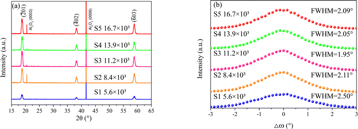 |
| | Fig. 1 XRD patterns of the β-Ga2O3 films grown at different VI/III ratios: (a) 2θ-ω scan; (b) rocking curves. | |
Surface morphology
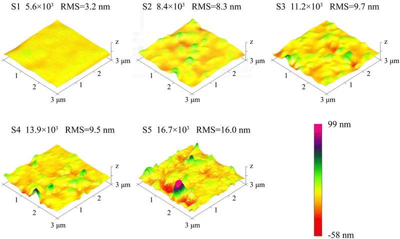
The AFM pictures of the β-Ga2O3 films is illustrated in Fig. 2. S1 displays a relatively smooth surface with a root-mean-square (RMS) roughness of merely 3.2 nm. As the VI/III ratio increases, the emergence of more hillocks is observed, along with a corresponding increase in RMS roughness. Notably, at the VI/III ratio of 16.7 × 10³, a proliferation of micro-grains becomes apparent, and the RMS roughness surges to 16.0 nm. This alteration in surface morphology is attributed to an enhanced nucleation density. The nucleation density at the initial stage of epitaxial growth can be calculated using the following formula:| | N = A![[thin space (1/6-em)]](https://www.rsc.org/images/entities/char_2009.gif) exp(−ΔG/RT) exp(−ΔG/RT) | (4) |
where N symbolizes the nucleation density, A is a constant, ΔG represents the activation free energy for nucleation, R is the Boltzmann constant, and T denotes the thermodynamic temperature of the substrate. ΔG is composed of the bulk free energy ΔGV and the surface free energy ΔGS, with ΔGV being inversely related to the partial pressure of O2, and ΔGS being inversely related to the O2 concentration.29–31 In this study, the O2 flow was increased to improve the VI/III ratio, leading to an increase in both the partial pressure and concentration of O2. Consequently, the nucleation density increased with the enhanced VI/III ratio, resulting in both the increased number of hillocks and the rise in RMS roughness.
 |
| | Fig. 2 AFM pictures of the β-Ga2O3 films grown at different VI/III ratios. | |
Surface chemical composition
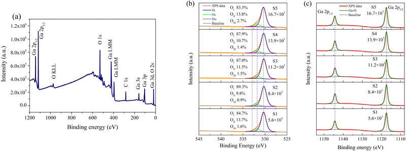
To delve into the surface chemical composition of the fabricated β-Ga2O3 films, XPS was employed. To erase the effects of sample charging, all binding energies presented were calibrated using the C 1s peak at 284.6 eV, originating from surface contamination. Fig. 3a shows the full scan of S1, detecting signals solely related to Ga, O, and C. Fig. 3b details the O 1s spectra for samples S1 to S5, exhibiting pronounced shoulders and tailings on the high-energy side. A deconvolution of the spectra was performed using Voigt line-shape and Shirley baseline, with the FWHM of each component held equal. The O 1s spectra could be deconvoluted into three distinct components: a major component at 530.3 eV (OI), a subordinate one at 531.9 eV (OII), and a minor one at 532.9 eV (OIII). OI and OIII can be distinctly attributed to Ga–O bonding and chemisorbed species, respectively, while the assignment of OII remains a subject of debate.23–26 In prior researches on the time-resolved detection performance of β-Ga2O3-based PDs, OII has commonly been assigned to O2− ions in oxygen-deficient regions due to VO,10–13,15,16 even some directly attribute OII to VO.17–19,32,33 However, such interpretations have notable limitations. Firstly, OII signals originate from the inner electrons of O atoms, but vacancies lack the electrons, thus precluding OII from arising directly from VO. Additionally, from S2 to S5, the O2 flow was doubled, but the proportion of OII increased from 9.8% to 13.8%, which is clearly in conflict with the view that OII originates from oxygen-deficient regions due to VO. Furthermore, VO should exert direct effects on Ga but O spectra, yet the peaks of Ga 2p1/2 and Ga 2p3/2, as shown in Fig. 3c, are able to be deconvolute into a single component attributable to Ga–O bonding, with no correlation to OII. Therefore, OII is suggested to be independent of VO. Based on our previous researches, OII can be ascribed to surface lattice O atoms.34,35 The binding energy for these O atoms at β-Ga2O3 surface lattice is elevated due to dangling bonds, leading to the formation of high-energy shoulders in the XPS spectra. Similarly, due to the absence of coordinated Ga atoms, such lattice O atoms also exist at defects like dislocations and grain boundaries. The proportions of OII and the RMS roughness of the films show a strong correlation; as RMS roughness increases, the specific surface area of the samples enlarges, leading to an increase in the proportion of surface lattice O atoms. The only exception is sample S1, which has the lowest surface roughness but a high proportion of OII. According to the XRD findings, more dislocations and small-angle grain boundaries exist within S1, contributing to the high proportion of OII. After excluding OIII (chemisorbed species), the O/Ga atom ratios in the lattice calculated from O 1s and Ga 3d for samples S1 through S5 are 1.52, 1.50, 1.51, 1.50, and 1.47, respectively, closely matching the theoretical stoichiometric ratio of 1.5, with minor variations attributed to experimental error (within 5%). Despite an increase in O2 flow from 200 sccm to 600 sccm, all corresponding VI/III ratios exceed 5000, indicating that all films were grown in significantly O-rich atmospheres. Thus, variations in O2 flow had minimal impact on the O/Ga atom ratios. Additionally, certain studies have attributed OII to C–O bonding.36,37 However, attributing OII to C–O bonds would require excluding it from the calculation of the O/Ga atom ratios in the β-Ga2O3 lattice; accordingly, the O/Ga atomic ratios for S1–S5 would be 1.31, 1.35, 1.34, 1.34, and 1.26, respectively. This inference, suggesting an increase in VO despite a doubling of O2 supply from S2 to S5, lacks both theoretical and experimental plausibility.
 |
| | Fig. 3 XPS spectra of the β-Ga2O3 films grown at different VI/III ratios: (a) full scan; (b) O 1s; (c) Ga 2p. | |
Optical transmittance spectra
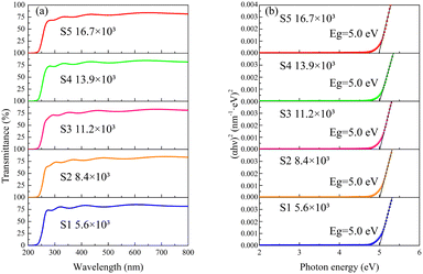
Fig. 4a displays the optical transmission spectra of the deposited β-Ga2O3 films. All samples exhibit sharp absorption edges ranging from 230 nm to 270 nm. Fig. 4b illustrates the optical bandgaps (Egs) of the films, calculated using Tauc's plot method.38 The Egs of the β-Ga2O3 films are consistently 5.0 eV, underscoring their promising potential for SBUV PD applications.
 |
| | Fig. 4 (a) Optical transmittance spectra of the β-Ga2O3 films grown at different VI/III ratios; (b) optical bandgaps of the films calculated by Tauc's plot method. | |
Luminescent propetries
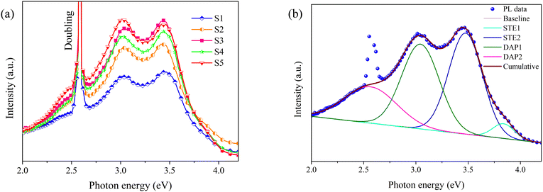
Fig. 5a displays the PL spectra of S1–S5, acquired using a 240 nm (5.17 eV) laser as the excitation source. The spectra can be broadly delineated into three components: the self-trapped exciton (STE) recombination emission centered around 3.4 eV, the donor–acceptor pair (DAP) recombination emission near 3.1 eV, and a laser doubling peak at 2.58 eV (480 nm).39 Consistent with the findings of the XRD analysis, the luminescence intensities of S2–S5 spectra exhibit close similarity, whereas the luminescence intensity of S1 is markedly diminished. This disparity can be ascribed to the inferior crystalline quality of S1, a large number of defects that serve as non-radiative recombination centers exist within the film.38 To gain a more detailed understanding of these PL spectra, a deconvolution using a Gaussian line-shape was carried out. Fig. 5b illustrates the deconvolution for the spectrum of S1, which is composed of four distinct emission peaks at 3.8 eV (STE1), 3.4 eV (STE2), 3.0 eV (DAP1), and 2.7 eV (DAP2). Based on the research conducted by Ho et al., STE1 and STE2 originate from distinct exciton recombination within β-Ga2O3. Regarding DAP1 and DAP2, Ga interstitial (Gai) functions as the donor, while Ga–O vacancy pairs (VGa + VO) and Ga vacancies (VGa) act as acceptors, respectively.40 The deconvolution for the spectra of S2–S5 are provided in Fig. S1 (ESI†). Table 2 outlines the proportion of each emission peak. The results indicate that STE2 and DAP1 are the primary contributors to the spectra, with their proportions exceeding 34.0% each. The propotions of different emission peaks across each sample exhibits slight variations and does not display a discernible pattern.
 |
| | Fig. 5 (a) The PL spectra of S1–S5; (b) the deconvolution for the PL spectrum of S1. | |
Table 2 The proportion of each emission peak for S1–S5
| Sample |
STE1 (%) |
STE2 (%) |
DAP1 (%) |
DAP2 (%) |
| S1 |
3.6 |
38.8 |
36.2 |
21.3 |
| S2 |
6.3 |
34.9 |
36.8 |
22.0 |
| S3 |
4.5 |
36.3 |
37.9 |
21.3 |
| S4 |
4.2 |
36.4 |
39.8 |
19.6 |
| S5 |
3.4 |
36.4 |
38.1 |
22.0 |
SBUV photodetectors
MSM PDs were fabricated using the obtained β-Ga2O3 films, the schematic diagram of the PDs is shown in Fig. 6a.
 |
| | Fig. 6 (a) The schematic diagram of the SBUV PDs; (b) the I254 and Idark of the PDs; (c) the I254 measured at 20 V bias of the PDs. | |
I
dark and I254.
The current–voltage (I–V) characteristics of the PDs were measured in the dark and under 254 nm illumination, with an illumination power density of 1.75 mW cm−2. The resulting I–V curves are shown in Fig. 6b. All PDs exhibit I254/Idark ratios on the order of 105. The I254 of each PD at 20 V bias are illustrated in Fig. 6c. The I254 of device fabricated with S1 (DS1) is significantly lower the the others. Due to the inferior crystalline quality, DS1 harbors an increased number of defects which function as recombination centers. This results in the quenching of photo-generated carriers and leads to the diminished photo response of the PD.41
Time-resolved detection performance.
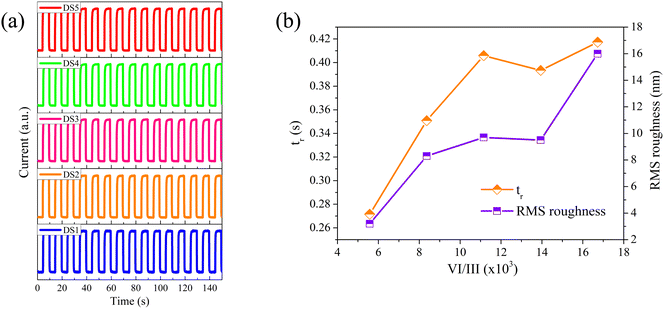
The time-resolved detection performance of the fabricated PDs was measured under 254 nm illumination and 20 V bias. As depicted in Fig. 7a, all the PDs demonstrate excellent repeatability and stability, with the current rapidly responding to the toggling of SBUV irradiation. Table 3 presents the 10–90% rise time (tr) and the 90–10% decay time (td) for each PD, averaging over five cycles. Two distinct phenomena are observed: (i) from DS1 to DS5, the tr progressively increases, and (ii) the td values are relatively short, fluctuating around 0.1 seconds without a pronounced PPC effect. To ensure the reliability of these phenomena, we prepared two additional PDs with the same structure for each β-Ga2O3 film and conducted repetitive experiments. The experimental results have verified the reliability of the phenomena.
 |
| | Fig. 7 (a) The time-resolved photocurrent response of DS1–DS5 measured under 254 nm illumination and 20 V bias; (b) the related tr and the RMS roughness of the β-Ga2O3 films grown at different VI/III ratios. | |
Table 3 The average tr and td of the SBUV PDs
| PD |
t
r (s) |
t
d (s) |
| DS1 |
0.272 |
0.116 |
| DS2 |
0.351 |
0.110 |
| DS3 |
0.406 |
0.087 |
| DS4 |
0.393 |
0.107 |
| DS5 |
0.417 |
0.078 |
The prolongation of tr or td is generally attributed to an increase in VO.10–12,15–19 However, from S1 to S5, despite tripling the O2 flow, the O/Ga atom ratio varied minimally, indicating that VO is not the cause of the increased tr. We believe that the increase in surface trap states leads to the extension of tr. Dangling bonds in surface atoms are capable of forming surface trap states, which trap carriers and extend tr.42–44 In this study, the films were grown under extremely O-rich conditions, and the PDs performance was tested under ambient conditions. Therefore, the dangling bonds on the surface Ga atoms can be readily passivated by O2, suggesting that surface traps are primarily composed of dangling bonds at the surface O atoms. With an increase in the VI/III ratio, the roughness of the obtained films increased, as shown in Fig. 7b, which in turn increased the surface area and the number of surface trap states.
Regarding phenomenon ii, to better analyze the recovery behavior of the PDs, we compare the performance of DS3 with that of our reported PD based on β-Ga2O3 homepitaxial film (DH).45 The FWHM of the XRD rocking curve for the homoepitaxial β-Ga2O3 film is less than 0.007°. As shown in Table 4, the tr and td of DS3 are significantly shorter than those of DH. The growth temperatures, pressures, and VI/III ratios during the growth processes of S3 and the homoepitaxial film are identical, and the O/Ga atom ratio of the homoepitaxial film is 1.51 (Fig. S2 in ESI†), hence, it is unreasonable to assume a higher concentration of VO in DH. Therefore, we believe that there are additional factors influencing the PPC effect of β-Ga2O3-based PDs, beyond VO. Moreover, in our another study involving β-Ga2O3 films grown by MOCVD on sapphire wafers, with the XRD rocking curve FWHM of the β-Ga2O3 film decreased from 1.85° to 1.40°, yet the corresponding td of the PDs increased from 0.061 s to 0.537 s. These findings indicate that as the crystalline quality of the β-Ga2O3 film improves, the corresponding PD's PPC effect also intensifies. We attribute this to the intrinsic band structure characteristics of β-Ga2O3. Research on the band structure has indicated that β-Ga2O3 can be considered an indirect semiconductor in terms of recombination.2,5,46,47 As a result, the transition of electrons from the conduction band minimum (CBM) to the valence band maximum (VBM) requires the involvement of phonons, and the direct band-to-band recombination rate is sluggish. Consequently, the relatively swift indirect recombination processes mediated by recombination centers expedites the recovery of β-Ga2O3-based PDs.39 As the crystalline quality improves, defects like dislocations, which function as recombination centers within the film, diminish.48–50 This diminishment leads to a higher proportion of direct recombining, thereby resulting in strong PPC. From this vantage point, the PPC of β-Ga2O3 is governed by a distinct mechanism compared to the commonly reported PPC of its amorphous countrapart, given that no existing studies have suggested the presence of an indirect bandgap in amorphous GaOX.51–53 Furthermore, although high crystalline quality can augment the PPC, it often results in higher photoelectric responsivity. Since both high photoelectric response and high response/recovery speed are crucial for an outstanding PD, achieving a balance between the two remains a challenge. Introducing a small number of deep-level impurities through doping engineering without compromising film quality may offer an effective solution, akin to doping gold atoms in silicon.54
Table 4 Comparison of the performance of DS3 and DH measured at 20 V bias
| PD |
t
r (s) |
t
d (s) |
Ref. |
| DH |
13.43 |
14.01 |
36
|
| DS3 |
0.406 |
0.087 |
This work |
Photoresponse spectra.
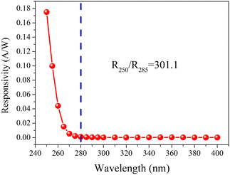
Fig. 8 illustrates the photoresponse spectra of DS5, measured at a 20 V bias. The PD exhibits excellent selectivity for SBUV irradiation. The cutoff wavelength is established at 280 nm, with a marked increase in responsivity observed from 280 nm to 250 nm. The responsivity at 250 nm (R250) and 285 nm (R285) are 1.75 × 10⁻¹ A W−1 and 5.81 × 10⁻⁴ A W−1, respectively, yielding a R250/R285 ratio of 301.1. Table 5 displays the comparson of the parameters for DS5 and a part of reported β-Ga2O3-based PDs. Compared with other devices, DS5 has advantages of swift recovery and high Iphoto/Idark.
 |
| | Fig. 8 The photoresponse spectrum of DS5 measured at 20 V bias. | |
Table 5 Comparison of the parameters for DS5 and a part of reported β-Ga2O3-based PDs
| Type |
I
photo/Idark |
R (A W−1) |
Rejection |
t
r
|
t
d
|
Ref. |
| β-Ga2O3/MgO/Nb:SrTiO3 heterojunction (APD) |
/ |
5.9 × 10⁵ |
/ |
12.4 ns |
41.7 μs |
55
|
| ZnO/β-Ga2O3 core–shell (APD) |
/ |
1.3 × 10³ |
/ |
20 μs |
42 μs |
9
|
| β-Ga2O3/GaN heterojunction |
6.1 × 10⁴ |
3.05@0 V |
R
254/R400 = 5.9 × 10³ |
0.018 s |
/ |
56
|
| β-Ga2O3/SiC heterojunction |
63.31 |
0.18 |
/ |
0.65 s/7.8 s |
1.73 s/15.22 s |
57
|
| Vertical Schottky |
360 |
0.16 |
R
222/R350 > 104 |
0.5 s |
0.5 s |
58
|
| MSM |
/ |
1.45 |
R
254/R365 ∼ 10.8 |
0.58 s/32.93 s |
1.2 s/32.86 s |
59
|
| MSM |
4 |
210 |
R
232/R320 = 5 × 10⁴ |
3.2 s |
1.4 s |
60
|
| MSM |
>105 |
1.05 |
/ |
4.5 |
2.2 |
61
|
| MSM |
∼105 |
1.75 × 10⁻¹ |
R
250/R285 = 301.1 |
0.417 s |
0.078 s |
This work |
Conclusions
In summary, SBUV PDs were fabricated utilizing β-Ga2O3 films grown via MOCVD. Through surface chemical analysis, we demonstrate that the sub-intense component observed in the O 1s spectra is not associated with VO, thereby rendering them inappropriate for characterizing VO in the investigation of time-resolved detection performance of β-Ga2O3-based PDs. Regarding the time-resolved characteristics of the PDs, our comparative analysis between the PD performance and the film properties has shed light on the fact that, aside from VO, the indirect bandgap of β-Ga2O3 also plays a pivotal role in the PPC of β-Ga2O3-based PDs, which distinguishes the PPC mechanism of β-Ga2O3 from that of its amorphous countrapart. Furthermore, we have identified that surface traps can lead to an extension of the tr. Note that, due to the insignificant change in the concentration of VO observed in this study, the discussion on the impact of VO on the time-resolved response characteristics of β-Ga2O3-based PDs is not included in this study. This study is instrumental in guiding the optimization and design of β-Ga2O3-based SBUV PDs.
Author contributions
Zeming Li: conceptualization, methodology, writing – original draft, investigation, funding acquisition. Rensheng Shen: investigation. Wancheng Li: methodology, conceptualization. Teng Jiao: visualization. Yuchun Chang: funding acquisition. Hongwei Liang: funding acquisition. Xiaochuan Xia: supervision. Baolin Zhang: conceptualization, methodology.
Data availability
The data supporting this article have been included in the main text.
Conflicts of interest
There are no conflicts to declare.
Acknowledgements
This research was funded by Liaoning province natural science foundation joint fund (doctoral research initiation project), Grant Number 2023-BSBA-028, the Fundamental Research Funds for the Central Universities, Grant Number DUT24BS008, Guangdong Basic and Applied Basic Research Foundation, Grant Number 2023A1515110064, the National Key Research and Development Program of China, Grant Number 2023YFB4503003, the National Natural Science Foundation of China, Grant Numbers 11975066 and 62104024, Dalian municipal bureau of science and technology, Grant Number 2020RT01, Special projects for industrial foundation reconstruction and high-quality development of manufacturing industry in 2022 (No. TC220A04A-49).
Notes and references
- X. Hou, Y. Zou, M. Ding, Y. Qin, Z. Zhang, X. Ma, P. Tan, S. Yu, X. Zhou, X. Zhao, G. Xu, H. Sun and S. Long, J. Phys. D: Appl. Phys., 2020, 54, 043001 CrossRef.
- J. B. Varley, J. R. Weber, A. Janotti and C. G. Van de Walle, Appl. Phys. Lett., 2010, 97, 142106 CrossRef.
- Z. Liu, P.-G. Li, Y.-S. Zhi, X.-L. Wang, X.-L. Chu and W.-H. Tang, Chin. Phys. B, 2019, 28, 017105 CrossRef CAS.
- H. Kim, SN Appl. Sci., 2021, 4, 27 CrossRef.
- Z. Li, T. Jiao, J. Yu, D. Hu, Y. Lv, W. Li, X. Dong, B. Zhang, Y. Zhang, Z. Feng, G. Li and G. Du, Vacuum, 2020, 178, 109440 CrossRef CAS.
- X. Chen, F.-F. Ren, J. Ye and S. Gu, Semicond. Sci. Technol., 2020, 35, 023001 CrossRef CAS.
- Y. J. Jeong, J. Y. Yang, C. H. Lee, R. Park, G. Lee, R. B. K. Chung and G. Yoo, Appl. Surf. Sci., 2021, 558, 149936 CrossRef CAS.
- T.-F. Weng, M.-S. Ho, C. Sivakumar, B. Balraj and P.-F. Chung, Appl. Surf. Sci., 2020, 533, 147476 CrossRef CAS.
- B. Zhao, F. Wang, H. Chen, Y. Wang, M. Jiang, X. Fang and D. Zhao, Nano Lett., 2015, 15, 3988–3993 CrossRef CAS.
- T. K. O. Vu, D. U. Lee and E. K. Kim, Nanotechnology, 2020, 31, 245201 CrossRef CAS.
- J. Wang, X. Ji, Z. Yan, S. Qi, X. liu, A. Zhong and P. Li, J. Alloys Compd., 2024, 970, 172448 CrossRef CAS.
- L. Deng, H. Hu, Y. Wang, C. Wu, H. He, J. Li, X. Luo, F. Zhang and D. Guo, Appl. Surf. Sci., 2022, 604, 154459 Search PubMed.
- X. Chen, W. Mi, M. Li, J. Tang, J. Zhao, L. Zhou, X. Zhang and C. Luan, Vacuum, 2021, 192, 110422 CrossRef CAS.
- X.-X. Li, G. Zeng, Y.-C. Li, Q.-J. Yu, M.-Y. Liu, L.-Y. Zhu, W. Liu, Y.-G. Yang, D. W. Zhang and H.-L. Lu, Nano Res., 2022, 15, 9359–9367 CrossRef CAS.
- L.-X. Qian, Z.-H. Wu, Y.-Y. Zhang, P. T. Lai, X.-Z. Liu and Y.-R. Li, ACS Photonics, 2017, 4, 2203–2211 CrossRef CAS.
- J. Wang, Y. Xiong, L. Ye, W. Li, G. Qin, H. Ruan, H. Zhang, L. Fang, C. Kong and H. Li, Opt. Mater., 2021, 112, 110808 CrossRef CAS.
- S. Feng, J. Li, L. Feng, Z. Liu, J. Wang, C. Cui, O. Zhou, L. Deng, H. Xu, B. Leng, X. Q. Chen, X. Jiang, B. Liu and X. Zhang, Adv. Mater., 2023, 35, 2308090 CrossRef CAS.
- L. Huang, Q. Feng, G. Han, F. Li, X. Li, L. Fang, X. Xing, J. Zhang and Y. Hao, IEEE Photonics J., 2017, 9, 1–8 Search PubMed.
- R. Xu, X. Ma, Y. Chen, Y. Mei, L. Ying, B. Zhang and H. Long, Mater. Sci. Semicond. Process., 2022, 144, 106621 CrossRef CAS.
- V. Brinzari, Appl. Surf. Sci., 2017, 411, 437–448 CrossRef CAS.
- M. Madel, F. Huber, R. Mueller, B. Amann, M. Dickel, Y. Xie and K. Thonke, J. Appl. Phys., 2017, 121, 124301 CrossRef.
- Z. G. Yin, X. W. Zhang, Z. Fu, X. L. Yang, J. L. Wu, G. S. Wu, L. Gong and P. K. Chu, Phys. Status Solidi RRL, 2012, 6, 117–119 CrossRef CAS.
- Q. Cao, L. He, H. Xiao, X. Feng, Y. Lv and J. Ma, Mater. Sci. Semicond. Process., 2018, 77, 58–63 CrossRef CAS.
- P. Song, Z. Wu, X. Shen, J. Kang, Z. Fang and T.-Y. Zhang, CrystEngComm, 2017, 19, 625–631 RSC.
- Z. Feng, L. Huang, Q. Feng, X. Li, H. Zhang, W. Tang, J. Zhang and Y. Hao, Opt. Mater. Express, 2018, 8, 2229–2237 CrossRef CAS.
- Y. J. Lee, M. A. Schweitz, J. M. Oh and S. M. Koo, Materials, 2020, 13, 434 CrossRef CAS.
- Z. Li, T. Jiao, D. Hu, Y. Lv, W. Li, X. Dong, Y. Zhang, Z. Feng and B. Zhang, Coatings, 2019, 9, 281 CrossRef CAS.
- C. Seitz, Z. G. Herro, B. M. Epelbaum, R. Hock and A. Magerl, J. Appl. Crystallogr., 2006, 39, 17–23 CrossRef CAS.
- C. Wu, D. Y. Guo, L. Y. Zhang, P. G. Li, F. B. Zhang, C. K. Tan, S. L. Wang, A. P. Liu, F. M. Wu and W. H. Tang, Appl. Phys. Lett., 2020, 116, 072102 CrossRef CAS.
- P. Bundle, Int. J. Electron., 1968, 24, 405–413 CrossRef.
- X. Liu, X. Wu, H. Cao and R. P. H. Chang, J. Appl. Phys., 2004, 95, 3141–3147 CrossRef CAS.
- P. Li, H. Shi, K. Chen, D. Guo, W. Cui, Y. Zhi, S. Wang, Z. Wu, Z. Chen and W. Tang, J. Mater. Chem. C, 2017, 5, 10562–10570 RSC.
- Z. Xi, L. Yang, Z. Liu, S. Yao, L. Shu, M. Zhang, S. Li, Y. Guo and W. Tang, J. Phys. D: Appl. Phys., 2023, 57, 085101 CrossRef.
- Z. Li, T. Jiao, W. Li, Z. Wang, Y. Chang, R. Shen, H. Liang, X. Xia, G. Zhong, Y. Cheng, F. Meng, X. Dong, B. Zhang, Y. Ma and G. Du, Appl. Surf. Sci., 2024, 652, 159327 CrossRef CAS.
- W. Li, C. Shen, G. Wu, Y. Ma, Z. Gao, X. Xia and G. Du, J. Phys. Chem. C, 2011, 115, 21258–21263 CrossRef CAS.
- H. Cui, Q. Sai, H. Qi, J. Zhao, J. Si and M. Pan, J. Mater. Sci., 2019, 54, 12643–12649 CrossRef CAS.
- R. Chen, D. Wang, J. Liu, B. Feng, H. Zhu, X. Han, C. Luan, J. Ma and H. Xiao, Cryst. Growth Des., 2022, 22, 5285–5292 CrossRef CAS.
- D. Hu, S. Zhuang, Z. Ma, X. Dong, G. Du, B. Zhang, Y. Zhang and J. Yin, J. Mater. Sci.: Mater. Electron., 2017, 28, 10997–11001 CrossRef CAS.
- L. Binet and D. Gourier, J. Phys. Chem. Solids, 1998, 59(8), 1241–1249 CrossRef CAS.
- Q. D. Ho, T. Frauenheim and P. Deák, Phys. Rev. B, 2018, 97, 115163 CrossRef CAS.
-
E. Liu, B. Zhu and J. Luo, The Physics of Semiconductors, 2011, pp. 95–102, 132–143 Search PubMed.
- B. Mallampati, S. V. Nair, H. E. Ruda and U. Philipose, J. Nanopart. Res., 2015, 17, 176 CrossRef.
- L. Li, E. Auer, M. Liao, X. Fang, T. Zhai, U. K. Gautam, A. Lugstein, Y. Koide, Y. Bando and D. Golberg, Nanoscale, 2011, 3, 1120–1126 RSC.
- X. Zhao, P. Tu, J. He, H. Zhu and Y. Dan, Nanoscale, 2018, 10, 82–86 RSC.
- Z. Li, T. Jiao, W. Li, G. Deng, W. Chen, Z. Li, Z. Diao, X. Dong, B. Zhang, Y. Zhang, Z. Wang and G. Du, Opt. Mater., 2021, 122, 111665 CrossRef CAS.
- C. Janowitz, V. Scherer, M. Mohamed, A. Krapf, H. Dwelk, R. Manzke, Z. Galazka, R. Uecker, K. Irmscher, R. Fornari, M. Michling, D. Schmeißer, J. R. Weber, J. B. Varley and C. G. V. d Walle, New J. Phys., 2011, 13, 085014 CrossRef.
- H. Peelaers and C. G. Van de Walle, Phys. Status Solidi B, 2015, 252, 828–832 CrossRef CAS.
- M. Albrecht, A. Cremades, J. Krinke, S. Christiansen, O. Ambacher, J. Piqueras, H. P. Strunk and M. Stutzmann, Phys. Status Solidi B, 1999, 216, 409–414 CrossRef CAS.
- M. Albrecht, H. P. Strunk, J. L. Weyher, I. Grzegory, S. Porowski and T. Wosinski, J. Appl. Phys., 2002, 92, 2000–2005 CrossRef CAS.
- Y. Ohno, T. Taishi and I. Yonenaga, Phys. Status Solidi A, 2009, 206, 1904–1911 CrossRef CAS.
- Z. Zhang, X. Zhao, X. Zhang, X. Hou, X. Ma, S. Tang, Y. Zhang, G. Xu, Q. Liu and S. Long, Nat. Commun., 2022, 13, 6590 CrossRef CAS PubMed.
- R. Li, W. Wang, Y. Li, S. Gao, W. Yue and G. Shen, Nano Energy, 2023, 111, 108398 CrossRef CAS.
- R. Zhu, H. Liang, S. Hu, Y. Wang and Z. Mei, Adv. Electron. Mater., 2021, 8, 2100741 CrossRef.
-
X. Meng and C. Kang, The Physics of semiconductors, 1993, pp. 211–221 Search PubMed.
- Q. Zhang, N. Li, T. Zhang, D. Dong, Y. Yang, Y. Wang, Z. Dong, J. Shen, T. Zhou, Y. Liang, W. Tang, Z. Wu, Y. Zhang and J. Hao, Nat. Commun., 2023, 14, 418 CrossRef CAS PubMed.
- D. Guo, Y. Su, H. Shi, P. Li, N. Zhao, J. Ye, S. Wang, A. Liu, Z. Chen, C. Li and W. Tang, ACS Nano, 2018, 12, 12827–12835 CrossRef CAS.
- Y. Qu, Z. Wu, M. Ai, D. Guo, Y. An, H. Yang, L. Li and W. Tang, J. Alloys Compd., 2016, 680, 247–251 CrossRef CAS.
- F. Alema, B. Hertog, P. Mukhopadhyay, Y. Zhang, A. Mauze, A. Osinsky, W. V. Schoenfeld, J. S. Speck and T. Vogt, APL Mater., 2019, 7, 022527 CrossRef.
- S. Oh, Y. Jung, M. A. Mastro, J. K. Hite, C. R. Eddy, Jr. and J. Kim, Opt. Express, 2015, 23, 28300–28305 CrossRef CAS PubMed.
- F. Alema, B. Hertog, O. Ledyaev, D. Volovik, G. Thoma, R. Miller, A. Osinsky, P. Mukhopadhyay, S. Bakhshi, H. Ali and W. V. Schoenfeld, Phys. Status Solidi A, 2017, 214, 1600688 CrossRef.
- Y. Li, D. Zhang, R. Lin, Z. Zhang, W. Zheng and F. Huang, ACS Appl. Mater. Interfaces, 2018, 11, 1013–1020 CrossRef PubMed.
|
| This journal is © The Royal Society of Chemistry 2025 |
Click here to see how this site uses Cookies. View our privacy policy here.  *a,
Hongwei
Liang
 *a,
Xiaochuan
Xia
a and
Baolin
Zhang
*b
![[thin space (1/6-em)]](https://www.rsc.org/images/entities/char_2009.gif) 414 cm3 mol−1, Pbub is the pressure inside the stainless steel bubbler, nO is the molar flow of O atoms, and FO represents the flow rate of O2.27
414 cm3 mol−1, Pbub is the pressure inside the stainless steel bubbler, nO is the molar flow of O atoms, and FO represents the flow rate of O2.27
![[2 with combining macron]](https://www.rsc.org/images/entities/char_0032_0304.gif) 01) reflection for the β-Ga2O3 samples. The full width at half maximum (FWHM) of these curves suggests that samples S2 through S5 can be grouped together, with minimal variation in FWHM, indicative of similar crystalline qualities. In contrast, sample S1 exhibits a substantially higher FWHM, pointing to a higher density of dislocations and small-angle grain boundaries within the film.28 The XRD data imply that a lower supply of O2 adversely affects the epitaxial growth of β-Ga2O3 films.
01) reflection for the β-Ga2O3 samples. The full width at half maximum (FWHM) of these curves suggests that samples S2 through S5 can be grouped together, with minimal variation in FWHM, indicative of similar crystalline qualities. In contrast, sample S1 exhibits a substantially higher FWHM, pointing to a higher density of dislocations and small-angle grain boundaries within the film.28 The XRD data imply that a lower supply of O2 adversely affects the epitaxial growth of β-Ga2O3 films.

![[thin space (1/6-em)]](https://www.rsc.org/images/entities/char_2009.gif) exp(−ΔG/RT)
exp(−ΔG/RT)