
 Open Access Article
 This Open Access Article is licensed under a Creative Commons Attribution-Non Commercial 3.0 Unported Licence
A wiping-type semiconductor–liquid generator utilizing water-bearing solid materials and hydrated biological tissues†
Zhaoqi
Liu
ab,
Shiquan
Lin
c,
Peng
Yang
ab,
Siyao
Qin
ab,
Jun
Hu
ab and
Xiangyu
Chen
 *ab
*ab
aBeijing Institute of Nanoenergy and Nanosystems, Chinese Academy of Sciences, 100083 Beijing, China. E-mail: chenxiangyu@binn.cas.cn
bSchool of Nanoscience and Engineering, University of Chinese Academy of Sciences, 100049 Beijing, China
cSchool of Mechanical Engineering, Beijing Institute of Technology, Beijing 100081, China
First published on 30th July 2024
Abstract
The charge generation due to the interaction between solids and liquids is an important branch for microenergy collection. This work presents a wiping-type semiconductor–liquid generator, which provides an ultrahigh transferred charge density of 186 mC m−2. Underwater Kelvin probe force microscopy reveals that different aggregation states of water molecules on the surface of both metals and silicon result in different interfacial dipole moments and surface fields, which greatly change the output voltage of the device. The generator has a free-standing working mode with no wire-connection to the movable liquid, and the utilization of water-bearing solid materials constrains the liquid in a more controllable state, which can enhance the robustness and the scope of application of the device. Accordingly, it can be used to harvest energy from the frictional motion of hydrated biological tissues, including both tongue licking and eyelid blinking. A smart contact lens is also fabricated and an average current density of 0.05 A m−2 is obtained from the eyelids of rabbits. This work expands the application fields of solid–liquid generators and the physical analysis of underwater surface potential can also elucidate various electronics processes happening on the liquid–semiconductor interface.
Broader contextThis work introduces a novel wiping-type semiconductor–liquid generator, presenting a breakthrough in microenergy harvesting. By achieving an ultrahigh transferred charge density of 186 mC m−2, this device enables the direct collection of triboelectric energy from hydrated biological tissues, exemplified by a smart contact lens and energy harvesting from rabbit eyelids. This development expands the application fields of solid–liquid generators, pushing the boundaries of micro–nano energy harvesting and sensing. Moreover, through underwater Kelvin probe force microscopy, the study offers valuable insights into the physical analysis of surface potential under different aggregation states of water molecules on various surfaces, shedding light on a broader understanding of energy generation processes at solid–liquid interfaces. The proposed free-standing working mode, eliminating the need for wire connection to the liquid, significantly broadens the applicability of this wiping generator, opening new possibilities for energy harvesting from a range of kinetic motions, including those exhibited by biological systems. These advancements not only enhance our capacity to harness mechanical energy but also pave the way for more sustainable and robust energy harvesting strategies, with potential implications across energy and environmental science. |
Introduction
Water, which covers over 70% of the earth's surface, contains vast amounts of energy to be exploited in rivers, lakes and oceans.1–3 Traditionally, electromagnetic generators are the most widely used technique to achieve high power generation from the mechanical energy of water, but they also exhibit drawbacks such as high cost, large volume, and poor robustness. In the micro-energy harvesting field, a lot of studies have been carried out to harvest energy from movable water in diversified forms, such as droplets,4–6 stream,7,8 or even vapours.9,10 Accordingly, an evaporation-based power generator has been proposed to generate energy from vapours,11,12 while a salinity gradient power generator13,14 can provide continuous current output based on ion immigration in water. As for the mechanical energy collection from micro/tiny fluids, the most representative methods are droplet-based triboelectric nanogenerators15–20 (TENGs) and tribovoltaic nanogenerators21,22 (TVNG). Both techniques achieve notable energy output from the charge generation process happening on liquid–dielectric and liquid–semiconductor interfaces, respectively. These approaches effectively collect energy from water and various applications have been reported based on these diversified droplet generators, including liquid sensors,23,24 smart windows,25,26 self-powered clothing27,28 and so on. However, the energy conversion efficiency of these liquid-based electricity generators is still constrained by many drawbacks of the liquids. Thus, it is still necessary to develop more effective and more durable energy harvesting strategies to fully utilize the mechanical energy at the solid–liquid interface.However, there are several unresolved scientific issues, which hinder the further development of liquid/fluid energy harvesting. Firstly, the physical understanding of the charge transfer and ionization process at a solid–liquid interface is rather limited,29 and there are not enough experimental methods to clarify the electrical process happening at the very interface of solid–liquid contact, including both an insulator and conductive solid.30–33 The influence of localized electric fields on liquid energy output remains unclear, and a thorough investigation of this phenomenon could potentially guide the study of performance modification. Additionally, the operation modes for collecting the kinetic energy of a liquid are relatively limited due to the highly variable shape34,35 of liquids and thus, the robustness of the solid–liquid energy generator is rather weak, compared with a solid–solid type generator. For example, the kinetic energy of water droplets is collected by exploiting the contact and separation motion of water droplets on a flat solid surface, while there are still issues with splashing and residual droplets. These unhandy working modes also greatly restrict the application scope of liquid–solid generators.
In this paper, we present a wiping-type semiconductor–liquid generator (wiping generator) to produce high energy density from the frictional motion between water-bearing solid materials and semiconductors. The utilization of water-bearing solid materials constrains the liquid in a more controllable state, which can enhance the robustness of the device and finally lead to an ultrahigh charge density. The measured output charge density of 186 mC m−2 has set a new record surpassing previous results achieved by both TVNG and TENG. Moreover, using underwater Kelvin probe force microscopy (KPFM), we are able to observe a potential drop induced by the different aggregation states of water molecules on the surface of different metals and silicon. The observation of this underwater surface field can elucidate physical understanding of all the energy generators involving solid–liquid interfaces. In addition, a free-standing working mode is designed without the need for a wire connection to the liquid, which greatly expands the applicability of this wiping generator. Accordingly, it can be used to harvest energy from the frictional motion of hydrated biological tissues, including both tongue licking and eyelid blinking. These devices expand the application fields of solid–liquid generators and exemplify their potential in the field of micro–nano energy or sensing.
Results and discussion
The design concept of this wiping generator utilizing solid materials bearing water and semiconductors is illustrated in Fig. 1a, where the wiping motion of an absorbent cloth across the top surface of the device can generate notable current between two electrodes. Different from traditional TVNGs and droplet generators, ultrahigh energy density has been achieved through structural design and operation modifications. When the water-bearing solid comes into contact with the top electrode, although the insulation layer still exists, water acts as a conductor to connect the upper electrode with the semiconductor, forming a circuit. This interaction precipitates the genesis of a current loop, which originates from the semiconductor's upper surface and is directed towards the lower electrode. This results in the induction of a pulse current, which serves to neutralize the built-in field present at each interface. Then, as the water-bearing solid slides or moves away, the current loop is interrupted until the next contact occurs. Due to the softness of the absorbent cloth and the lubricating effect of water, the device exhibits excellent durability. The inset Fig. 1a(i) and (ii) depict the surface scanning electron microscopy (SEM) images of both the traditional solid–solid sliding TVNG and the wiping-type generator after undergoing 30 sliding cycles. As for the material selection for the wiping object, it is necessary to consider softness, high absorbency, fine villous microstructure, and durability. Table S1 (ESI†) illustrates our experimental attempts with various materials, including absorbent cloth, paper, regular silk, printing paper, and foam plastic. The absorbent cloth made of ultra-fine fibers (eyeglass cloths) was chosen for conducting our experiments in order to achieve optimal and outstanding results. As shown in Fig. 1b, the presence of water initially induces a change in the surface potential of Al and Si, leading to the formation of a new equilibrium of charge carriers. The wiping process, as well as the subsequent evaporation process, disrupts this equilibrium, resulting in the movement of electrons and holes. At this moment, the circuit is established, and an output current is generated to the external environment. Fig. 1b also shows the structural design and operational principle of the device. Specifically, both the top and bottom electrodes are attached on the surface of the Si substrate. The top electrode is separated from the Si substrate by an insulating buffer layer to prevent the direct formation of heterostructures. This design buries the wires underneath the semiconductor silicon, creating a compact structure and free-standing working mode. In the initial state, the charge carriers within the silicon wafer reach equilibrium in their natural state. Then, when the absorbent cloth connects the Al electrode and Si, a new equilibrium is established. Next is rapidly wiping, and this motion disrupts the equilibrium, causing the ions within the water bridge to experience polarization between the Al and Si, resulting in the generation of a current loop from the top surface of the semiconductor to the bottom electrode. Finally, as the absorbent cloth leaves the surface of the device, any residual traces of water evaporate, returning the system to its initial state. The equivalent circuit of this process is depicted in Fig. 1c. In the absence of a wet conductor connection on the device surface (due to the weak ionization of DI water, it can act as a conductor), the entire circuit remains open. Capacitor C1 is formed between the Si substrate and the lower electrode. Additionally, capacitor C2 is formed between the upper surface of the Si and the aluminum (Al) electrode. The overall circuit impedance is denoted as RG. However, the situation changes when a conductor connects the Si substrate with the Al electrode. In this case, water forms a capacitor (C3) and also closes the circuit. This connection also increases the resistance of the water, denoted as RW.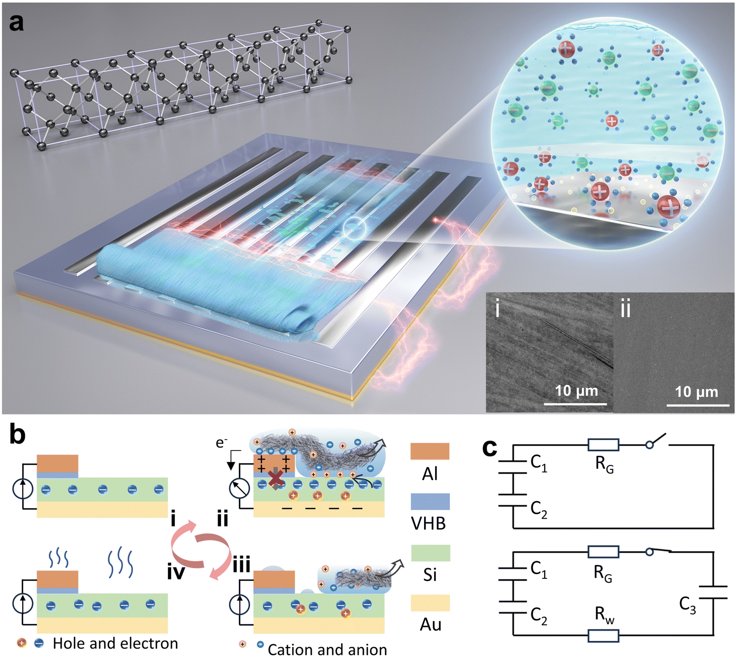 | ||
| Fig. 1 The general structure of a wiping-type semiconductor–liquid generator utilizing water-bearing solid materials. (a) The operation status of the wiping generator. (The inset graphs (i) and (ii): SEM comparison of the wiping type generator and a traditional solid–solid sliding TVNG.) (b) The working mechanism of the wiping generator. (The ions inside the water bridge undergo polarization between Al and Si, leading to the generation of a current loop from the top surface of the semiconductor to the bottom electrode.) (c) The capacitance model of the wiping generator when wiping. | ||
A diagram showing the disassembled structure of the wiping-type generator is shown in Fig. 2a. It consists of a four-layer structure, and the specific production method can be found in the Methods section. A flat Si wafer is utilized as the substrate, where HF (hydrofluoric acid) solution is employed for pretreatment to remove the surface oxide layer. The X-ray energy spectrum indicates a significant reduction in the concentration of oxygen element on the surface of the treated Si wafer (the result is shown in the ESI,† Fig. S1). A layer of aurum (Au) electrode is magnetron sputtered onto the unpolished surface of the Si wafer to serve as the bottom electrode. For the top electrode, conductive Al is employed, and there is an ultra-thin insulating polyacrylate adhesive (VHB) between Al and Si as a buffer layer. Absorbent cloth, which is highly flexible and filled up with water, establishes excellent contact between the Al and the Si wafer through a water bridge. The insulated buffer layer separates Al and Si, preventing them from forming a heterojunction in the initial state. By integrating Al and Si into a fixed terminal through the insulating layer, the wiping process with an absorbent cloth is utilized to generate and remove water bridges. This structural design eliminates the need for a moving electrode and forms a compact structure, simplifying the entire device and expanding its potential applicability. Furthermore, we have employed a grating shaped top electrode to achieve a larger water-bridging contact area between Al and Si. Fig. 2b–e exhibit the ultra-high energy density output of the wiping generator. The open-circuit voltage and peak power density of the wiping generator at different resistances from 100 Ω to 50 kΩ are shown in Fig. 2b. The maximum peak power density reaches 2.9 W m−2 with a load of 2 kΩ. More importantly, even though the output voltage is limited by the insufficient dielectric properties of semiconductors, this wiping generator demonstrates superior output current and ultrahigh transferred charge density, as shown in Fig. 2c and d. The effective area during sliding corresponds to the exposed surface area of the Si wafer. For a device with dimensions of 1 × 1 cm2, where half of the area is covered by electrodes, the effective contact area would be 0.5 cm2. Consequently, the calculated charge density is 186 mC m−2, and the current density is 9.6 A m−2. With capacitive charging, the capacitors of 4.7 μF, 10 μF, 20 μF, 30 μF and 50 μF are charged for 6 s with a wiping frequency of 0.3 Hz, as shown in Fig. 2e. To demonstrate its high charge density, as shown in the ESI,† Video S1 and Fig. 2f, the 1 × 1 cm2 device can power a LED using a circuit management device. This device operates with the help of a multi-stage boost circuit that takes advantage of the characteristics of multiple parallel-switching channels and energy storage elements capable of maintaining a constant voltage across their terminals while storing energy. Through series–parallel conversion, the device gradually transfers energy to the next stage. When switches S1–8 are closed, the wiping generator charges four capacitors C1–4 (4.7 μF) simultaneously to approximately 0.5 V. Then, when S1–8 are opened and S9–12 are closed, the power stored in the four capacitors is quickly transferred to the LED, and four 0.5 V capacitors connected in series are sufficient to light up the LED. By using this switching method, one wiping motion is enough to light up the LEDs, demonstrating an ultra-high charge density.
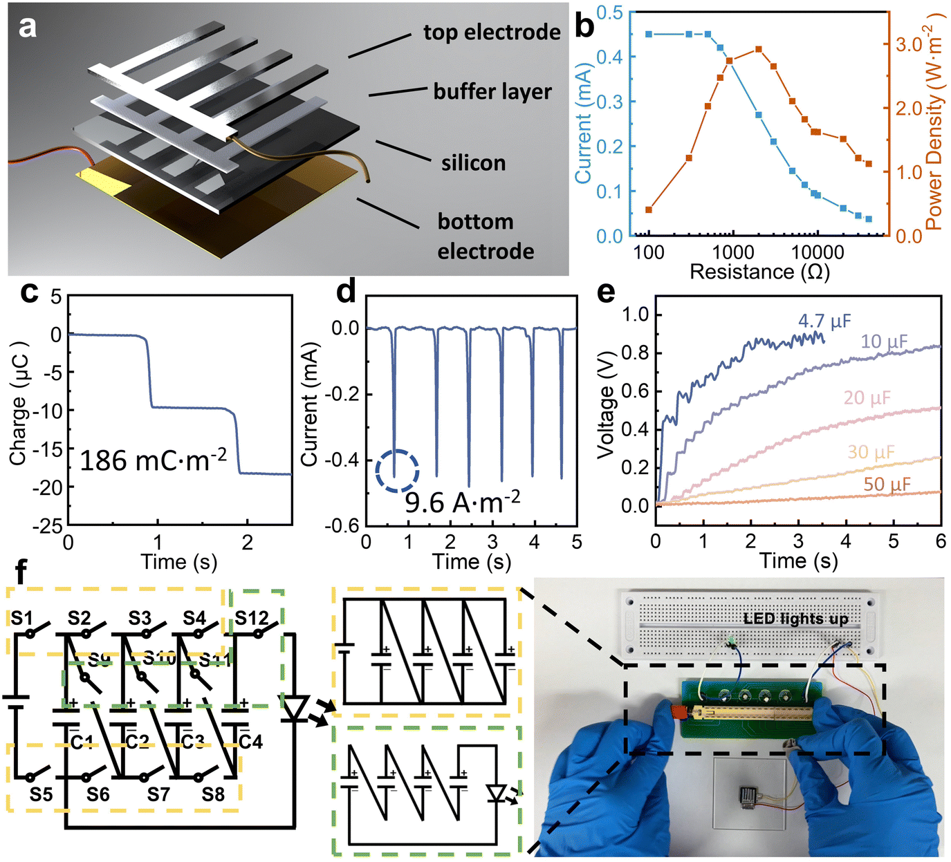 | ||
| Fig. 2 High performance demonstration of the wiping type semiconductor–liquid generator. (a) The dismantled structure of the wiping generator. (b)–(d) The transfer charge, short-circuit current and peak power density of the wiping generator. (e) Charging curve of a 4.7 μF, 10 μF, 20 μF, 30 μF and 50 μF capacitor using the wiping generator for 6 s. (f) The wiping generator uses a circuit management system to light up a LED. | ||
To optimize the working performance of the wiping generator, various control parameters of the device have been studied. ICP etching is used to create micro nano structures on the Si surface to increase its contact area. As shown in Fig. 3a, after the etching, the generator fabricated with the Si wafer exhibits a slight increase in current compared to the unetched one, which is attributed to the increased effective contact area. Although the surface of Si becomes more hydrophobic, in our structure, water is confined within the absorbent cloth and tightly pressed against the surface of the Si wafer, resulting in an enlarged contact area. In addition to Si wafers, several other commonly used semiconductors, such as GaAs, InP, and GaN, are tested and the related open-circuit voltage is shown in Fig. 3b. While GaAs offers the highest voltage, the current density is not significantly high. Therefore, in our experiments, we opt to use single-crystal silicon as the substrate material. Similar to Si, these semiconductors demonstrate excellent capabilities for direct current output when employed as substrates, demonstrating the universal applicability of this structure for energy harvesting in other semiconductors. In fact, for the wiping generator, due to the combined effect of the electrode and silicon wafer ions in water inducing charges, there is an optimal ratio of the silicon wafer and electrode area to achieve maximum output. Therefore, we fix the electrode area at 10 mm2 and gradually reduce the surface area of Si to measure the current density, obtaining an increase in current density from 1.5 A m−2 to 16 A m−2. By conducting experiments with different liquids as the medium, it has been found that the electrical conductivity of the liquids significantly affects the current output. The electrical resistivity of various liquids is provided in the ESI,† Table S2, and as depicted in Fig. 3d, where C2H5OH exhibits a considerably low conductivity due to its low ion concentration in solution, resulting in a significantly low output current. However, as the conductivity increases, a 1 M Na2CO3 solution demonstrates a high output current as 0.5 mA. The increase in solution conductivity leads to more ions being polarized between the Si and Al, thereby facilitating the migration of more charge carriers and resulting in increased current. Moreover, it is found that during measurements, both NaCl and Na2CO3 solutions lead to a decrease in the stability of the output. Additionally, due to the potential corrosiveness of NaCl and Na2CO3 solution towards metal electrodes, we do not recommend their practical application. Compared with TENG and TVNG devices, the advantage of this wiping generator is the ultrahigh output current and transferred charge density. As marked in Fig. 3f, g and Tables S2, S3 (ESI†), the maximum output charge density of this wiping generator is 1.3 times that of the highest previous records.15–20,36–48 Different from traditional TENG and TVNG, it has the merit of a special operational mode, resulting in distinct output characteristics. Compared with the solid–liquid generator, the charge density also far exceeds the previous TENG and DEG. It is also necessary to point out that the output voltage of this wiping generator (around 1.0 V) is jeopardized by the insufficient dielectric performance of the semiconductor and the overall power density of this wiping generator is also influenced by this low output voltage. However, by conducting a thorough and comprehensive mechanistic analysis, it is possible to further improve the output voltage and ultimately achieve an increase in power generation. However, compared with traditional TVNG and TENG, this wiping generator has these advantages: liquid lubrication on the semiconductor surface provides higher durability for the generator; its structure reduces the dependence of mobile terminals on wires, making the generator more suitable for applications in complex scenarios, and the fixed shape of the liquid increases the robustness of the entire device.
 | ||
| Fig. 3 Factors that affect the output of the wiping generator. (a) The influence of surface etching on Si wafers. (b) The voltage output when using different semiconductor materials as substrates. (c) The output current density of the wiping generator under different exposed Si areas. (d) The effect of soaking solution on current density. (e) The influence of Si wafer resistivity on current density. (f) A transfer charge density comparison with previous studies of TVNGs and TENGs. (g) A transfer charge density comparison with previous studies of solid–liquid generators. | ||
To investigate the working mechanism of the wiping generator, we used Kelvin probe force microscopy (KPFM) to measure the surface potentials of several metals. The surface potential of Si, Al, Ag, Zn, Ni, and the reference Au in the air was measured by KPFM in a conventional manner, and as shown in Fig. 4a–f. However, to our surprise, the output voltage of the wiping generators made from these metals exhibit no consistent correlation with the difference in surface potential (ϕ) between the metals and Si, which inspire us to consider the key role of water in this process. In order to rule out the contribution of triboelectrification to the operation, we further study several influencing parameters of this wiping generator. When the device is wiped with the same absorbent cloth but when it is either wet or dry, there is a significant difference in the generated current with a magnitude variation over 1000 times (as shown in Fig. 4g), which fully demonstrates that liquids play a decisive role in the power generation device. As depicted in Fig. 4h, the heterojunction of Al/deionized (DI) water/n-Si displays favorable rectification characteristics when a bias voltage ranging from −1 to 2 V is applied in the contacted state. This behavior can be attributed to the heterojunction behavior at the liquid–semiconductor interface. The enlarged output signal of the wiping generator is shown in Fig. 4i. When the water-bearing cloth contacts with the device, the circuit closes and the appearance of the water bridge leads to a new equilibrium of charge carriers, resulting in a weak current signal. As the water-bearing cloth is wiped across the surface of the generator, the old equilibrium is disrupted and a new equilibrium is formed. The ions in the water bridge are induced to reorganize, with negative ions induced near Al and positive ions induced near Si. At the same time, opposite charges are also induced on the two electrodes, causing sharp current signals to be generated through external circuits. The absorbent cloth slides over the surface of the device, causing a large area change (ΔS) in a short period of time. When the ΔS due to the coverage of absorbent cloth reaches its maximum value, the current also reaches its peak value.
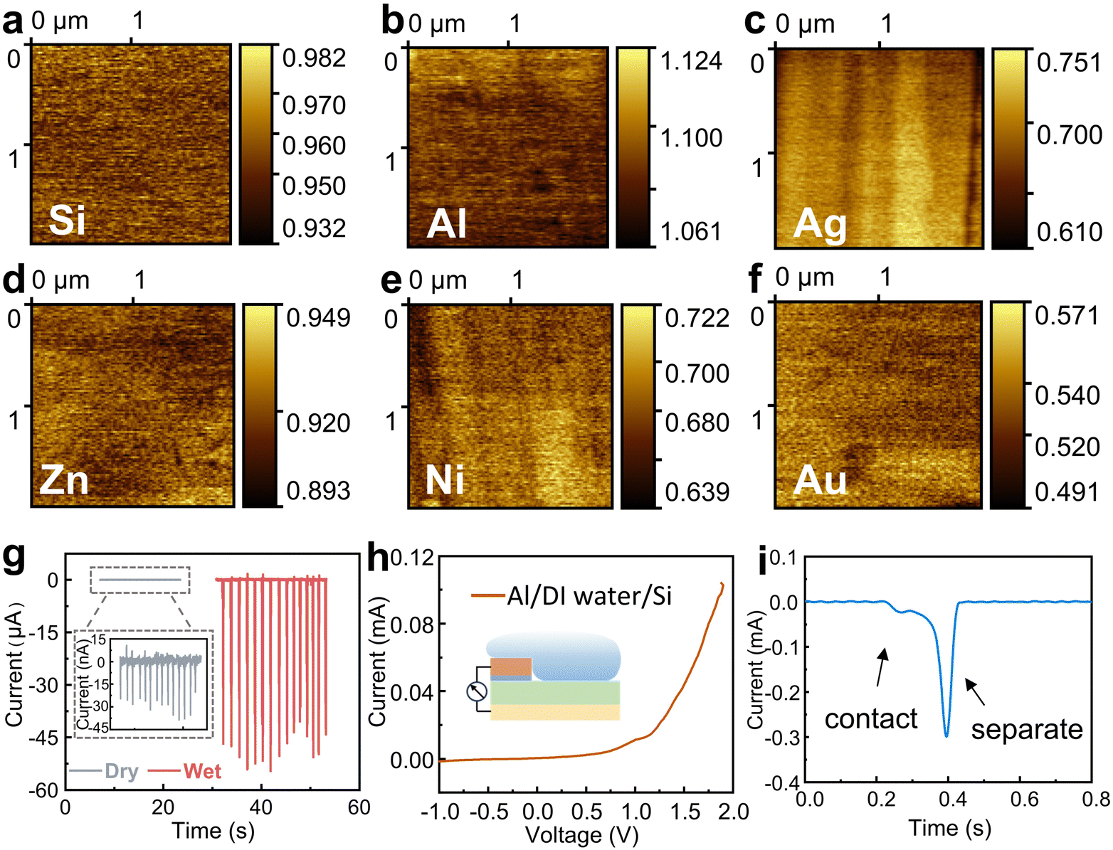 | ||
| Fig. 4 The physical mechanism of the wiping generator to improve the energy density of generators. (a)–(f) The surface potential of Si and metals Al, Ag, Zn, Ni, and Au measured using KPFM in air. (g) I–V characteristic curve of the generator in the contact state from −1 to 2 V. (h) Comparison of the wiping mode wiping generator output using either a dry or wet absorbent cloth for wiping. (i) A detailed variation diagram of the current. | ||
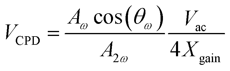
Previous studies related to liquid–semiconductor generators have seemingly overlooked the influence of the water dipole on the output performance of the generator. In this work, the underwater surface potential is measured by using a self-made dual harmonic Kelvin probe force microscope (DH-KPFM), as shown in Fig. 5a. In the DH-KPFM measurements, the induced surface potential of the sample underwater is calculated by using the amplitude of the cantilever oscillation at ω and 2ω frequencies, as well as the phase shift of the cantilever oscillation at ω frequency. Instead of applying a direct current (DC) compensating bias, these measurements are performed without the application of a DC bias. Since no DC bias is applied, the ions or polar molecules in the liquid remain in a quasi-static state during the measurement and do not migrate or decompose. Therefore, DH-KPFM can be used in liquid environments, including polar liquids such as deionized (DI) water. The surface potential is ultimately calculated as follows:30,49
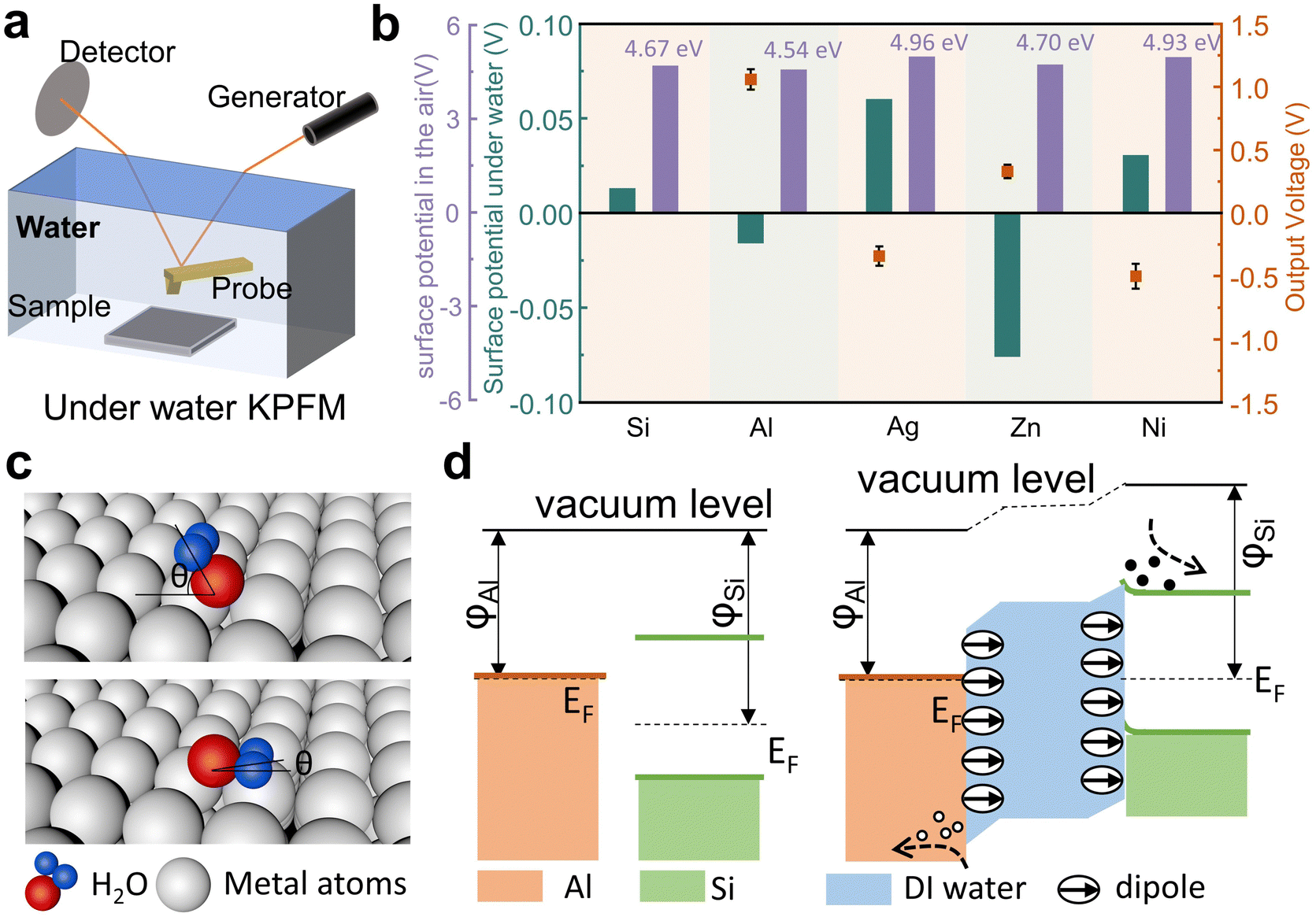 | ||
| Fig. 5 The influence of EDL on the work function of metals. (a) The diagram of the experimental setup of underwater KPFM. (b) The calculated surface potential under water, the surface potential of metal and Si in the air measured using KPFM, and the output voltage of the metal–Si wiping generator. (c) The principle of the surface potential of metals changes. (d) Band diagram of Schottky variations under water excitation. | ||
Fig. 5b summarizes the surface potential of metal and Si in the air, the induced surface fields (potential drop) underwater and the output voltage of the metal–Si wiping generator (the detailed data are given in the ESI,† Fig. S2). Due to the presence of water on the metal surfaces, the work functions of all these solid materials have been changed by the induced underwater interfacial potential. However, as depicted by the purple bars in the figure, the potential changes induced by water are different for each solid, and some may even exhibit an opposite polarity shift, such as Zn. Previous studies suggest that H-bonding and water–metal bonding are the primary factors controlling the structure of water coverage on metal surfaces.50 From a macroscopic potential characterization standpoint, our study provides evidence of the different aggregation states of water molecules on the surface of different metals. Therefore, we attribute these variations to the influence of the metal surface lattice on the dipole arrangement of water molecules on the metal surfaces, as shown in Fig. 5c. Different water–metal bonding causes the angle (θ) between the dipole plane of adsorbed water molecules and the metal surface to vary. The adsorbed water's dipole moment leads to changes in the surface fields (potential drop) of the metal under the influence of water. Therefore, the output voltage of the device is related to the combination value of the work functions of the metal and Si surface and the interfacial dipole moments at the solid–liquid interface. Here, the calculated underwater surface potential is probed at a distance of 50 nm from the solid surface. The detailed surface potential is not exactly equal to the work function change of the solid materials, but the polarity and the amplitude of the surface potential can be used as the reference to show the strength of the interfacial dipole. Taking Al (4.54 eV) as an example, water causes a decrease in the surface potential of Al and an increase in the surface potential of Si. This leads to an expansion of the difference in surface potentials between the two, ultimately resulting in the maximum output of the Al–Si wiping generator. Additionally, for the metal Zn (4.70 eV), water causes a significant decrease in the surface potential of Zn, leading to a reversal in voltage direction for the Zn–Si wiping generator, which further confirms our conclusion. It is important to note that by measuring the output voltage of the external circuit, we can only roughly determine the total potential drop across the whole device. Only by utilizing this kind of underwater KPFM, are we are able to directly test the specific variations in surface potential underwater for each solid material, leading to a complete physical picture of the device. Based on the aforementioned research, we summarize the working mechanism and principles of the wiping generator. Fig. 5d presents the energy band diagram of the wiping mode TENG. When there is no water as a medium in the structure, the Al and Si are actually completely separated because of the existence of an insulation buffer layer. The presence of a buffer layer has transformed the previous movable upper electrode into a fixed terminal, integrating the entire device into a free-standing unit. Then, when the water is a medium existing on the Al and Si surface, due to the weak ionization of water, the Al/DI water/Si form a heterojunction. Simultaneously, the interfacial dipole of water causes a shift at the Al/DI water and DI water/Si interfaces. In the p-type Al–Si wiping generator, the Fermi level (EF) of Al is higher than that of Si. When the water leads to the formation of heterojunctions between the two, electrons flow from Al to Si due to the difference in Fermi energy level. This results in the band on the Si side bending downwards, and the EF is aligned across the device and the vacuum level (Evac) offsets are established to compensate for the work function difference between adjacent layers. Meanwhile, the surface electric field caused by different dipole orientations of the water change the potential energy difference. However, the changes in surface potential caused by the adsorbed water dipoles vary for different metals. As shown in the ESI,† Fig. S3, for Zn, the effect of dipoles is similar to that of Al, resulting in a significant decrease in surface potential and a reversal in voltage direction for the Zn–Si wiping generator. On the other hand, for Ag and Ni, the effect of dipoles is opposite to that of Al, leading to an increase in surface potential and a decrease in their output voltage. The insights gained from our research can inspire future studies to explore the effective manipulation of the electric fields at the solid–liquid interfaces. By optimizing the electric fields at both the electrode and semiconductor surfaces, we can further enhance the output voltage of the wiping generator. This approach shows promise for achieving higher energy generation efficiency and advancing the field of solid–liquid power generation.
The free-standing mode of this wiping generator does not require a wire-connection to the mobile terminals and allows for its operation under wet conditions, significantly expanding its potential applications. In order to expand its applications, we have considered utilizing the wiping generator as a power source or sensory module for smart contact lenses,51 harnessing the energy generated from blinking. Fig. 6a shows the structure design and schematic images of the wiping generator being integrated into a smart contact lens. The contact lens is made of polydimethylsiloxane (PDMS) substrate,52 and a generator unit. In order to balance the compactness of the system, the power generation system on the contact lens is composed of 7 tiny wiping generation units connected in parallel. A flexible silicon wafer of 100 μm thickness is used as the substrate for the wiping generator to enhance its biocompatibility, and Fig. S4 (ESI†) showcases its exceptional flexibility. Each tiny wiping unit has a size of 1 × 2 mm, with an effective area of approximately 1 mm2. These micro generators are also comprised of an Au bottom electrode, Si substrate, VHB buffer layer, and Al top electrode. In order to minimize discomfort for biological applications, we have coated the edges of the silicon wafer with PDMS, creating an embedded structure with silicone as shown in Fig. S5 (ESI†). This design leaves only the upper surface exposed, ensuring a smooth surface for wiping. The circuit connecting these power generation units in parallel uses aerosol jet printing. Before printing, the surface of PDMS is cleaned with UV light to decrease its hydrophobicity. Fig. 6b and c depict the contact angle of the PDMS surface before and after UV treatment, demonstrating the enhanced affinity for ink adhesion, ensuring even distribution. Fig. 6d and Fig. S6 (ESI†) show the aerosol jet printing of the Ag circuit results in a strong adhesion, providing the circuit with excellent conductivity. Before the operation of the smart contact lens, we first demonstrate the feasibility of the energy generation from the sliding motion of hydrated biological tissues by using tongue licking (Fig. 6e), where a 3 cm × 3 cm wiping generator is used for the experiment. Indeed, the tongue is surrounded by saliva, making it a highly water-rich organ. This high moisture content makes it challenging to harness for energy generation using devices like TENGs. However, the tongue has shown remarkable potential for power generation and sensing applications in wiping generators. The results are shown in Fig. 6e and Video S2 (ESI†) and a stable current of approximately 4 μA can be produced during the tongue licking process, which confirms the feasibility of bioenergy harvesting. On this basis, we developed a sensor mask based on a wiping generator (Fig. S7, ESI†), aimed at promoting communication among paralyzed individuals. By placing four independent patch sensors on the inner surface of the mask, they can output signals separately. Four sensors located in different positions can be used for simple directional expressions such as “up, down, left, and right” through the licking action of the tongue. This sensor provides a new expression form for paralyzed patients with limited limb mobility. Through the licking action of the tongue, they can easily convey simple directional expressions. The design of the sensor allows for direct operation by utilizing the natural tongue movement of licking. This simplicity makes it accessible to a wide range of users and reduces the learning curve related to operating devices. Building upon the successful experiments with the tongue, a male New Zealand white rabbit was used for the in vivo experiments for the smart contact lens, as shown in Fig. 6g. Due to the unpredictable nature of rabbits, the experiments are conducted under anesthesia. The eyelids of the rabbits are manually guided during the experiment. To enhance moisture retention, protect the cornea, and reduce any potential discomfort during the experiment, sodium hyaluronate eye drops (Hylo-Comod) are applied to the surface of the rabbit's cornea before applying the contact lenses into the rabbit's eyes. Using the contact lens, an average output current of 0.16 μA is achieved, and the maximum current density is 0.05 A m−2, and the experimental process and results are shown in the ESI,† Video S3 and Fig. 6h. After the rabbit regains consciousness, it is observed for 24 hours, and no abnormalities in its eyes are detected. Capacitors can also be used to store this electrical energy (Fig. S8, ESI†), or the electrical energy can be directly supplied to other components on the contact lens, thereby reducing the inconvenience caused by wire transmission. These applications not only broaden the application fields of solid–liquid power generation and TVNG but also demonstrate the potential of this generator in the realm of micro–nano energy harvesting and sensing. It signifies the pioneering integration of a solid–liquid generator with hydrated biological tissue, facilitating direct interaction between generator and hydrated organisms. This breakthrough effectively addresses the inefficiency challenges faced by TENG under wet conditions and overcomes the inconvenience encountered when TVNG comes into contact with biological tissues.
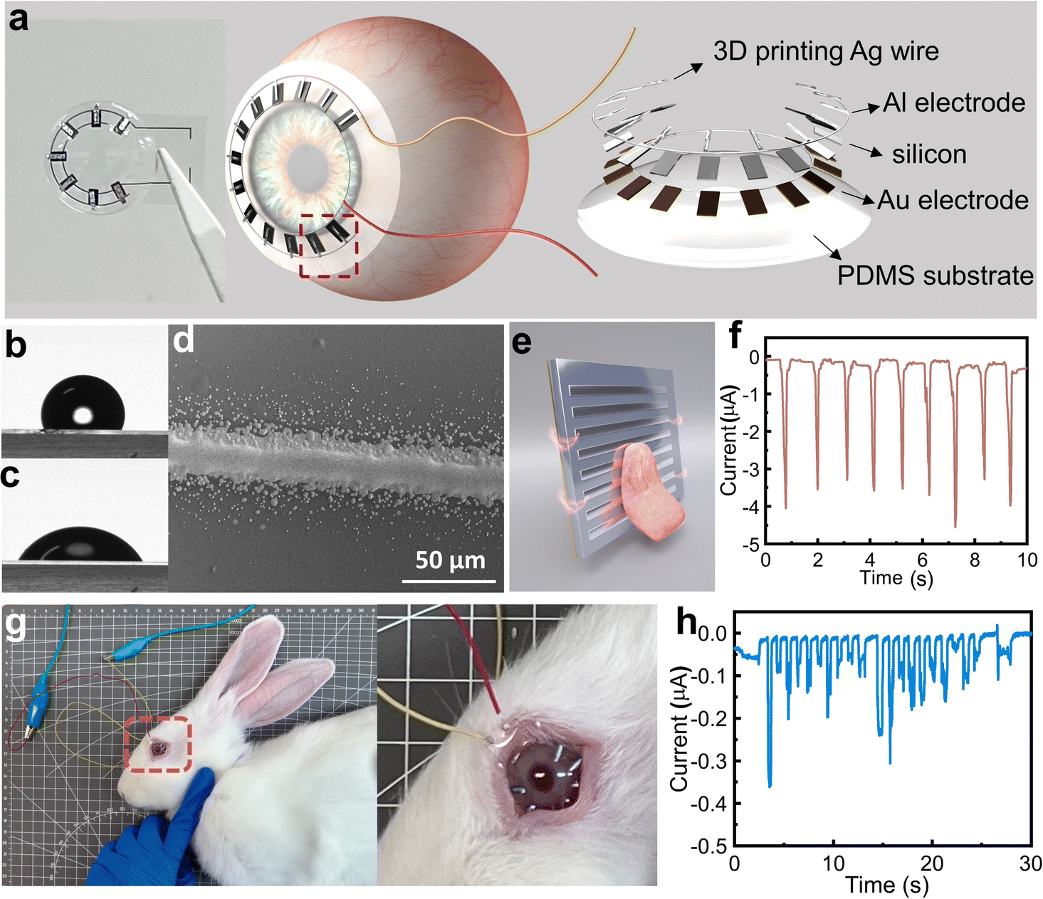 | ||
| Fig. 6 The wiping generator is applied to generate electricity from hydrated biological tissues. (a) The schematic and physical images of the wiping generator being made into smart contact lenses. (b) and (c) Hydrophilic properties of the PDMS substrate surface before and after UV treatment. (d) The SEM of aerosol jet 3D printing Ag wires. (e) and (f) Model and operating mechanism of tongue licking generates electricity. (g) Photographs of the in vivo test on a live rabbit using the soft, smart contact lens. (h) Diagram of energy output signal when the rabbit is blinking. | ||
Experimental
Materials
The single crystal Si〈100〉 wafers are n type with a thickness of 500 ± 25 μm and were bought from Wuxi Jingdian Semiconductor Materials Co., Ltd. The resistivity ranges from 0.001 to 0.01 Ω cm, from 1 to 10 Ω cm, from 10 to 20 Ω cm, and from 20 to 50 Ω cm, respectively. The Si wafers used for the smart contact lens are laser-cut into dimensions of 1 × 2 mm. These substrates have a resistivity range of 1 to 10 Ω cm and a thickness of 100 ± 10 μm.The single crystal GaN〈0001〉 wafer is n type with a thickness of 450 ± 50 μm, the single crystal GaAs〈100〉 to 〈111〉 wafer is n type with a thickness of 350 ± 25 μm, and the single crystal InP〈100〉 wafer is n type with a thickness of 350 ± 25 μm and they were bought from Wuxi Jingdian Semiconductor Materials Co., Ltd.
Hydrofluoric acid (HF, ≥40%) was purchased from Shanghai Aladdin Biochemical Technology Co., Ltd. NaCl (AR) and Na2CO3 (AR) were purchased from Shanghai Aladdin Biochemical Technology Co., Ltd, and they were not purified before use.
The metals used in the experiment were purchased from Fuxiang Metal Materials Co., Ltd.
VHB (9460) was purchased from Minnesota Mining and Manufacturing Company.
Fabrication of the wiping-type generator
To create the device, a flat Si wafer is utilized as the base substrate. Firstly, immerse the Si wafer in a 5% HF (hydrofluoric acid) solution for 10 minutes to remove the surface oxide layer. A layer of Au electrode is magnetron sputtered onto the unpolished surface of the Si wafer to serve as the bottom electrode. Next, place the Si wafer in a high-temperature furnace and anneal it at 550 °C. The annealing process will cause the Au electrode to become compact and tightly attached to the surface. Due to oxidation that may occur at high temperatures, it is necessary to immerse the wafer in HF again to remove any oxide layer formed on the surface. For the top electrode, conductive Al tape is employed, and there is an ultra-thin insulating polyacrylate adhesive (VHB) between Al and Si as a buffer layer.Fabrication of the smart contact lens
After mixing the PDMS (SYLGARD 184, Dow Corning) base component A and curing agent component B in a ratio of 10![[thin space (1/6-em)]](https://www.rsc.org/images/entities/char_2009.gif) :1, inject the mixture into the contact lens mold and place it in an oven at 60 °C for solidification. The circuit on the contact lens is made by aerosol jet printing at Beijing Yunshang Zhizao Technology Co., Ltd. Before printing, the PDMS surface is cleaned with UV light to reduce its hydrophobicity, allowing the ink to adhere evenly. The required circuits are printed on the contact lens using an aerosol printer and silver ink, controlled by a programmed system. The lens with printed circuits are then dried at 200 °C for 15 min, resulting in well-conductive circuits. The manufacturing process of the wiping generator is the same as in the previous part.
:1, inject the mixture into the contact lens mold and place it in an oven at 60 °C for solidification. The circuit on the contact lens is made by aerosol jet printing at Beijing Yunshang Zhizao Technology Co., Ltd. Before printing, the PDMS surface is cleaned with UV light to reduce its hydrophobicity, allowing the ink to adhere evenly. The required circuits are printed on the contact lens using an aerosol printer and silver ink, controlled by a programmed system. The lens with printed circuits are then dried at 200 °C for 15 min, resulting in well-conductive circuits. The manufacturing process of the wiping generator is the same as in the previous part.
Characterization and measurements
A programmable electrometer (Keithley 6514) was applied to test the output voltage, current, and transferred charge. An SEM (SU8020, Hitachi) equipped with EDS accessory was used to characterize the morphologies of the contact lens and generator. A source meter (Keithley 2450) was used to measure the current–voltage (I–V) of the generator, and the start and stop voltage were ranged from −1 V to 2 V. A sputter deposition platform (Discovery 635, Denton Vacuum) was used to deposit the Au bottom electrode. KPFM experiments were performed on commercial AFM equipment Multimode 8 (Bruker, USA). NSC 18 (MikroMash, USA; Au coated; tip radius: 25 nm; spring constant: 2.8 N m−1) was used as the conductive tip here. ICP etching was carried out using a SENTECH inductively coupled plasma etching machine (SI 500). A 10 nm layer of gold is sputtered onto the surface of the Si wafer. Subsequently, etching is performed for 600 s in an atmosphere containing SF6, O2, and Ar gases. The etching process is carried out using an ICP power of 800 W and an RF power of 50 W.Rabbit experiments
All experimental processes were strictly in line with the institutional and national guidelines for the care and use of laboratory animals and the study protocol was reviewed and approved by the Ethical Committee of Beijing Institute of Nanoenergy and Nanosystem (A-2019027&202401).For the in vivo experiments, male New Zealand white rabbits were used. The entire experimental process was conducted in a temperature-controlled room set at 30 °C to prevent hypothermia in the rabbits. The rabbits were intramuscularly injected with a combination of Rompun (5 mg kg−1) and ketamine (20 mg kg−1) prior to the start of the experiment, inducing general anesthesia. This anesthesia protocol was used to ensure that the rabbits were in a state of deep sedation throughout the entire procedure. The eyelids of the rabbits were manually guided during the experiment. To enhance moisture retention, protect the cornea, and reduce any potential discomfort during the experiment, sodium hyaluronate eye drops (Hylo-Comod) were applied to the surface of the rabbit's cornea before applying the contact lenses into the rabbit's eyes. After the rabbit regained its consciousness naturally, it was observed for 24 hours, and no abnormalities in its eyes were detected.
Conclusions
The wiping-type semiconductor–liquid generator presented in this work offers a promising solution for efficiently harnessing energy from movable water. This wiping generator takes advantage of water-bearing solid materials to confine the variable fluid, resulting in enhanced robustness and charge density. As for the design of the electrode, the top and bottom electrodes are made of different metal foils and a sandwich insulating layer is inserted between the top electrode and semiconductor, which leads to the free-standing working mode of this wipe generator. The contact between the water-bearing solid and the top electrode can generate a current loop from the top surface of the semiconductor to the bottom electrode and a pulse current is induced to neutralize the build-in field on each interface, while the sliding motion of the water-bearing solid breaks the current loop until the next contact. Different from traditional TENG and TVNG, this wiping generator has a distinct working mode and output characteristics. It demonstrates superior output current and ultrahigh transferred charge density. The maximum transferred charge density is 186 mC m−2, which is higher than all the previous records in both liquid-based TVNG and TENG. For a device with an effective working area of 0.5 mm2, it is capable of simultaneously charging four parallel-connected 4.7 μF capacitors to approximately 0.5 V with only one wipe, which is enough to light up a LED through a switching circuit. Meanwhile, the underwater KPFM is applied to study this wiping generator. The results show that the different metals and silicon exhibit quite different surface fields and potential drop under water and the aggregation states as well as the related dipole moments of water molecules on the surface of both metals and silicon is the underlying mechanism. This new observation accounts for many special output voltage signals obtained from different samples and it can also clarify various electronics processes happening at the liquid–semiconductor interface. In the case of Al, it experiences the highest voltage output due to the established positive surface potential underwater, which further decreases its work function. Accordingly, Al is so-far the best choice for the electrode.Moreover, the free-standing design of the mobile fluid in this generator significantly expands its potential applications. The tongue licking process is applied to this wiping generator and continuous energy generation can be demonstrated. Accordingly, the wiping generator has been applied for fabricating a smart contact lens, where 7 tiny wiping generators each with a size of 1 mm2 are integrated onto the lens by using an ultra-fine printing circuit, and an average current density of 0.05 A m−2 can be obtained from the eyes of rabbits. These applications not only broaden the scope of the solid–liquid power generator but also exemplify the generator's potential in the emerging field of micro–nano energy harvesting and sensing. The compact size, high energy density, and convenient free-standing operation make this generator suitable for various usage scenarios requiring portable energy sources. In conclusion, the wiping-type semiconductor–liquid generator presented in this paper provides a promising approach for efficiently harnessing energy from movable water sources. By utilizing water-bearing solid materials, this generator overcomes the limitations of traditional electromagnetic generators, achieving enhanced robustness and charge output. The record-breaking energy density, novel freestanding operation, and successful applications in hydrated biological tissues signify significant advancements in the field of solid–liquid power generation and highlight the potential for micro–nano energy harvesting and sensing. Continued research and development in this area will lead to even more efficient and versatile energy harvesting solutions.
Author contributions
Z. L. and X. C. conceived the idea. X. C., Z. L., and S. L. performed the data measurements. S. L. designed the KPFM experiments. Z. L. and P. Y. prepared the manuscript. J. H. and S. Q. offered assistance with the experiments. All the authors discussed the results and commented on the manuscript.Data availability
All data needed to evaluate the conclusions in the paper are present in the paper and/or the ESI.† Additional data related to this paper may be requested from the authors.Conflicts of interest
There are no conflicts to declare.Acknowledgements
We thank Helin Animal Hospital for providing the facilities and assisting us in conducting certain animal experiments. We thank Yunshang Zhizao Technology Co., Ltd for assisting us in completing the 3D circuit printing. This work is supported by the National Natural Science Foundation of China for Excellent Young Scholar (Grant No. 52322313), the National Natural Science Foundation of China (Grant No. 62174014, 52375213), the National Key R&D Project from Minister of Science and Technology (2021YFA1201601), the Beijing Nova program (No. 20230484399), the Youth Innovation Promotion Association CAS (2021165), the Innovation Project of Ocean Science and Technology (22-3-3-hygg-18-hy), the State Key Laboratory of New Ceramic and Fine Processing Tsinghua University (KFZD202202), the Fundamental Research Funds for the Central Universities (292022000337), and the Young Top-Notch Talents Program of Beijing Excellent Talents Funding (2017000021223ZK03).References
- J. Scruggs and P. Jacob, Science, 2009, 323, 1176–1178 CrossRef CAS PubMed.
- S. H. Salter, Nature, 1974, 249, 720–724 CrossRef.
- Z. L. Wang, Nature, 2017, 542, 159–160 CrossRef CAS PubMed.
- W. Xu, Y. Jin, W. Li, Y. Song, S. Gao, B. Zhang, L. Wang, M. Cui, X. Yan and Z. Wang, Sci. Adv., 2022, 8, eade2085 CrossRef CAS PubMed.
- D. Kam, G. Gwon, S. Jang, D. Yoo, S. J. Park, M. La and D. Choi, Adv. Mater., 2023, 35, 2303681 CrossRef CAS PubMed.
- Q. Zhang, Y. Li, H. Cai, M. Yao, H. Zhang, L. Guo, Z. Lv, M. Li, X. Lu, C. Ren, P. Zhang, Y. Zhang, X. Shi, G. Ding, J. Yao, Z. Yang and Z. L. Wang, Adv. Mater., 2021, 33, 2105761 CrossRef CAS PubMed.
- J. Xiong, M.-F. Lin, J. Wang, S. L. Gaw, K. Parida and P. S. Lee, Adv. Energy Mater., 2017, 7, 1701243 CrossRef.
- J. H. Ahn, J. Y. Hwang, C. G. Kim, G. H. Nam and K. K. Ahn, Nano Energy, 2020, 67, 104269 CrossRef CAS.
- Z. Zhang, X. Li, J. Yin, Y. Xu, W. Fei, M. Xue, Q. Wang, J. Zhou and W. Guo, Nat. Nanotechnol., 2018, 13, 1109–1119 CrossRef CAS PubMed.
- S. Gao and Z. Wang, Nat. Sustainability, 2023, 6, 1514–1515 CrossRef.
- X. Liu, T. Ueki, H. Gao, T. L. Woodard, K. P. Nevin, T. Fu, S. Fu, L. Sun, D. R. Lovley and J. Yao, Nat. Commun., 2022, 13, 4369 CrossRef CAS PubMed.
- L. Chen, J. Ren, J. Gong, J. Qu and R. Niu, Chem. Eng. J., 2023, 454, 140383 CrossRef CAS.
- Y. Guo, H. Huang, Z. Li, X. Wang, P. Li, Z. Deng and X. Peng, ACS Appl. Mater. Interfaces, 2019, 11, 35496–35500 CrossRef CAS PubMed.
- H. Jung, C. V. Subban, J. D. McTigue, J. J. Martinez, A. E. Copping, J. Osorio, J. Liu and Z. D. Deng, Renewable Sustainable Energy Rev., 2022, 160, 112283 CrossRef.
- Z. Liu, Y.-z Huang, Y. Shi, X. Tao, P. Yang, X. Dong, J. Hu, Z.-X. Huang, X. Chen and J.-P. Qu, Adv. Funct. Mater., 2023, 33, 2302164 CrossRef CAS.
- W. Tang, T. Jiang, F. R. Fan, A. F. Yu, C. Zhang, X. Cao and Z. L. Wang, Adv. Funct. Mater., 2015, 25, 3718–3725 CrossRef CAS.
- D. Wang, X.-X. Wang, M. L. Jin, P. He and S. Zhang, Nano Energy, 2022, 103, 107819 CrossRef CAS.
- J. Wang, H. Wu, S. Fu, G. Li, C. Shan, W. He and C. Hu, Nano Energy, 2022, 104, 107916 CrossRef CAS.
- W. Xu, H. Zheng, Y. Liu, X. Zhou, C. Zhang, Y. Song, X. Deng, M. Leung, Z. Yang, R. X. Xu, Z. L. Wang, X. C. Zeng and Z. Wang, Nature, 2020, 578, 392–396 CrossRef CAS PubMed.
- H. Zhang, K. Wang, J. Li, J. Li, R. Zhang and Y. Zheng, Matter, 2022, 5, 1466–1480 CrossRef CAS.
- Y. Li, Q. Zhang, Y. Cao, Z. Kang, H. Ren, Z. Hu, M. Gao, X. Ma, J. Yao, Y. Wang, C. Zhang, G. Ding, J. Liu, J. Bao, H. Wang and Z. Yang, Energy Environ. Sci., 2023, 16, 4620–4629 RSC.
- S. Lin, Y. Lu, S. Feng, Z. Hao and Y. Yan, Adv. Mater., 2019, 31, 1804398 CrossRef.
- W. Kim, D. Choi, J.-Y. Kwon and D. Choi, J. Mater. Chem. A, 2018, 6, 14069–14076 RSC.
- S. Lin, C. Liu, X. Chen, Y. Zhang, H. Lin, X. Yu, Y. Bo and Y. Lu, Research, 2023, 6, 0202 CrossRef CAS PubMed.
- H. Liu, Z. H. Guo, F. Xu, L. Jia, C. Pan, Z. L. Wang and X. Pu, Sci. Bull., 2021, 66, 1986–1993 CrossRef CAS PubMed.
- M. Timusk, J. Locs, T. Kangur, A. Kasikov, J. Kurnitski and A. Šutka, ACS Appl. Polym. Mater., 2023, 5, 5937–5950 CrossRef CAS.
- J. Wang, W. Yang, Z. Liu, Y. Su, K. Li, Y. Li, Q. Zhang, C. Hou and H. Wang, Nano Energy, 2023, 107, 108171 CrossRef CAS.
- E. G. Jeong, Y. Jeon, S. H. Cho and K. C. Choi, Energy Environ. Sci., 2019, 12, 1878–1889 RSC.
- A. Šutka, L. Lapčinskis, D. He, H. Kim, J. D. Berry, J. Bai, M. Knite, A. V. Ellis, C. K. Jeong and P. C. Sherrell, Adv. Mater. Interfaces, 2023, 10, 2300323 CrossRef.
- L. Collins, J. I. Kilpatrick, S. V. Kalinin and B. J. Rodriguez, Rep. Prog. Phys., 2018, 81, 086101 CrossRef PubMed.
- S. Lin, L. Xu, A. Chi Wang and Z. L. Wang, Nat. Commun., 2020, 11, 399 CrossRef CAS PubMed.
- W. Xu and Z. Wang, Joule, 2020, 4, 2527–2531 CrossRef.
- J. Li, Y. Long, Z. Hu, J. Niu, T. Xu, M. Yu, B. Li, X. Li, J. Zhou, Y. Liu, C. Wang, L. Shen, W. Guo and J. Yin, Nat. Commun., 2021, 12, 4998 CrossRef CAS PubMed.
- J. Tan, Z. Fan, S. Sun, M. Xu and D. Jiang, Adv. Mater. Interfaces, 2023, 10, 2202037 CrossRef.
- M. Wang, X. Wang, Y. Nan, H. Xu, H. Zhou, Y. Sun, P. Yi and T. Yu, Chem. Eng. J., 2023, 477, 146832 CrossRef CAS.
- L. Zhou, Y. Gao, D. Liu, L. Liu, Z. Zhao, S. Li, W. Yuan, S. Cui, Z. L. Wang and J. Wang, Adv. Energy Mater., 2021, 2101958 CrossRef.
- H. Wu, W. He, C. Shan, Z. Wang, S. Fu, Q. Tang, H. Guo, Y. Du, W. Liu and C. Hu, Adv. Mater., 2022, 34, 2109918 CrossRef CAS PubMed.
- Z. Zhang, Z. Wang, Y. Chen, Y. Feng, S. Dong, H. Zhou, Z. L. Wang and C. Zhang, Adv. Mater., 2022, 34, 2200146 CrossRef CAS PubMed.
- J. Meng, C. Pan, L. Li, Z. H. Guo, F. Xu, L. Jia, Z. L. Wang and X. Pu, Energy Environ. Sci., 2022, 15, 5159–5167 RSC.
- C. Shan, W. Liu, Z. Wang, X. Pu, W. He, Q. Tang, S. Fu, G. Li, L. Long, H. Guo, J. Sun, A. Liu and C. Hu, Energy Environ. Sci., 2021, 14, 5395–5405 RSC.
- Z. Wang, Z. Zhang, Y. Chen, L. Gong, S. Dong, H. Zhou, Y. Lin, Y. Lv, G. Liu and C. Zhang, Energy Environ. Sci., 2022, 15, 2366–2373 RSC.
- S. Fu, W. He, H. Wu, C. Shan, Y. Du, G. Li, P. Wang, H. Guo, J. Chen and C. Hu, Nano-Micro Lett., 2022, 14, 155 CrossRef CAS PubMed.
- W. Qiao, L. Zhou, Z. Zhao, P. Yang, D. Liu, X. Liu, J. Liu, D. Liu, Z. L. Wang and J. Wang, Nano-Micro Lett., 2023, 15, 218 CrossRef CAS PubMed.
- Y. Liu, W. Liu, Z. Wang, W. He, Q. Tang, Y. Xi, X. Wang, H. Guo and C. Hu, Nat. Commun., 2020, 11, 1599 CrossRef CAS PubMed.
- Z. Zhao, L. Zhou, S. Li, D. Liu, Y. Li, Y. Gao, Y. Liu, Y. Dai, J. Wang and Z. L. Wang, Nat. Commun., 2021, 12, 4686 CrossRef CAS PubMed.
- D. Liu, X. Yin, H. Guo, L. Zhou, X. Li, C. Zhang, J. Wang and Z. L. Wang, Sci. Adv., 2019, 5, eaav6437 CrossRef CAS PubMed.
- W. Qiao, Z. Zhao, L. Zhou, D. Liu, S. Li, P. Yang, X. Li, J. Liu, J. Wang and Z. L. Wang, Adv. Funct. Mater., 2022, 32, 2208544 CrossRef CAS.
- H. Wu, N. Mendel, S. van der Ham, L. Shui, G. Zhou and F. Mugele, Adv. Mater., 2020, 32, 2001699 CrossRef CAS PubMed.
- J. I. Kilpatrick, L. Collins, S. A. L. Weber and B. J. Rodriguez, Rev. Sci. Instrum., 2018, 89, 123708 CrossRef PubMed.
- J. Carrasco, A. Hodgson and A. Michaelides, Nat. Mater., 2012, 11, 667–674 CrossRef CAS PubMed.
- D. H. Keum, S.-K. Kim, J. Koo, G.-H. Lee, C. Jeon, J. W. Mok, B. H. Mun, K. J. Lee, E. Kamrani, C.-K. Joo, S. Shin, J.-Y. Sim, D. Myung, S. H. Yun, Z. Bao and S. K. Hahn, Sci. Adv., 2020, 6, eaba3252 CrossRef CAS PubMed.
- G. Yao, X. Mo, S. Liu, Q. Wang, M. Xie, W. Lou, S. Chen, T. Pan, K. Chen, D. Yao and Y. Lin, Nat. Commun., 2023, 14, 3604 CrossRef CAS PubMed.
Footnote |
| † Electronic supplementary information (ESI) available. See DOI: https://doi.org/10.1039/d4ee02797c |
| This journal is © The Royal Society of Chemistry 2024 |