 Open Access Article
Mixed 2D-cation passivation towards improved durability of perovskite solar cells and dynamics of 2D-perovskites under light irradiation and at high temperature†
Santa
Mondal‡
,
Naoto
Eguchi‡
 ,
Naoyuki
Nishimura
 ,
Yoyo
Hinuma
 ,
Kohei
Yamamoto
 ,
Atsushi
Kogo
 ,
Takurou N.
Murakami
* and
Hiroyuki
Kanda
 *
*
National Institute of Advanced Industrial Science and Technology (AIST), Tsukuba, Ibaraki 305-8565, Japan. E-mail: takurou-murakami@aist.go.jp; hiroyuki.kanda@aist.go.jp
First published on 21st November 2024
Abstract
A low-dimensional perovskite layer is important as a passivation layer for the 3D perovskite photo-absorber to increase the photovoltaic performance and stability. Here, we provide an effective passivation technique that enhances the durability of perovskite solar cells and investigate the impact of the 2D perovskite on the photovoltaic properties under light irradiation as well as high-temperature conditions. Our proposed mixed 2D cation (n-butylammonium iodide (BAI) and n-octylammonium iodide (OAI)) passivation can control the opto-electronic properties of the 2D perovskites and improve the durability of perovskite solar cells. Furthermore, our main finding is that the migration of the 2D perovskite into the 3D perovskite layer, during light and high-temperature stability tests, causes the reduction of the photovoltaic properties of the perovskite solar cells. This information suggests how to design the 2D perovskite layer leading to stable perovskite solar cells from the viewpoint of cation migration, which can be the novel design strategy for the 2D/3D perovskite system.
Introduction
Perovskite solar cells have progressed rapidly since their public release in 2009, breaking the previous record with a power conversion efficiency of over 26%.1–6 Hybrid organic–inorganic perovskite materials have excellent photo-electrical properties such as enhanced absorption coefficients, long electron–hole diffusion lengths, high defect tolerance, and flexible fabrication methods, leading to expectations of their practical application as next-generation solar cells.7–122D perovskites have been introduced as an excellent surface passivator for the 3D perovskite layer due to their stable crystal structure and hydrophobicity, which improved the stability of the perovskite solar cells.13–18 These low-dimensional crystals consist of metal halide octahedra separated by larger organic cations, so-called spacers, which can be classified as Ruddlesden popper (A′)2(A)n−1PbnX3n+1,19,20 Dion–Jacobson (A′′)(A)n−1PbnX3n+1,21 and alternating cation (B)(A)nPbnX3n+1 phase metal halide perovskite crystals.22 Therefore, there are a lot of crystal combinations of low-dimensional perovskite crystals that have the advantages of tunability of optical and electrical properties which affect the photovoltaic properties of perovskite solar cells.23,24 Recently, mixed spacers were introduced into the 2D perovskite layer that improved solar cell stability.25 The advantage is that different spacers can control the optoelectronic properties, which can further expand the structural combination of 2D perovskite engineering, and thus more tailored investigation is required.
On the other hand, understanding the crystal dynamics of 2D perovskites under stability testing is a key factor in further improving the durability of perovskite solar cells.26 F. Fiorentino et al. suggested that the crystal properties of a 2D perovskite on a 3D perovskite change dynamically under light irradiation and high temperature.27 Such crystal changes can affect the photovoltaic properties of perovskite solar cells. However, there is no investigation on the crystal changes of 2D perovskite crystals compared to the photovoltaic properties of perovskite solar cells. The reason why this research has not progressed to date may be the erroneous assumption that a 2D perovskite on a 3D perovskite layer is stable and the general lack of knowledge about the diffusion of 2D cations in the research community of perovskite solar cells. Thus, there is great value in comparing the photovoltaic performance and crystal structure of the perovskite layer in the course of the stability test, and such knowledge can help in establishing how to design 2D/3D perovskite solar cells.
In this work, we introduced mixed 2D cations for 2D/3D perovskite solar cells to increase their durability under light irradiation. A novel mixed 2D perovskite layer was formed by using n-octylammonium iodide (C8H17NH3·I) and n-butylammonium iodide (C4H11N·HI) on top of the 3D perovskite layer. Furthermore, the time-resolved 2D perovskite layer was compared to the photovoltaic properties of 2D/3D perovskite solar cells under light irradiation and high-temperature conditions, verifying the effect of crystal dynamics on the photovoltaic properties. We provide more insight into the 2D/3D system under the stability conditions.
Results and discussion
Characterization of the 2D perovskite layer
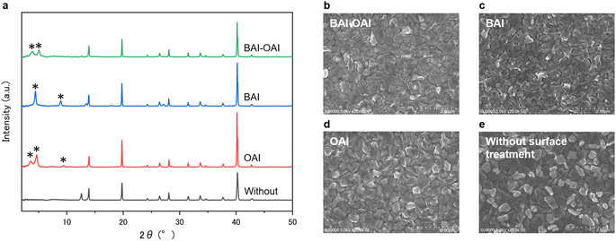
Herein, we investigated the effect of the mixed cation 2D perovskite at the interface of the 3D perovskite and hole-transport layer. Note that 2D perovskites using BAI, OAI, and the mixed solution were abbreviated to BAI, OAI, and BAI-OAI, respectively. X-ray diffraction (XRD) was used to measure the crystal structure of each perovskite film (Fig. 1). The samples were prepared as BAI/3D perovskite/SnO2/FTO, OAI/3D perovskite/SnO2/FTO, BAI-OAI/3D perovskite/SnO2/FTO, and 3D perovskite/SnO2/FTO. The BAI, OAI, and BAI-OAI samples showed 2D perovskite peaks below 10°, while 3D perovskite peaks emerged between 10 and 50°. The obtained spectra were assessed with the help of reported CIF files with VESTA. Regarding BAI samples, peaks were observed at 4.5 and 9.0°, which correspond to the (002) lattice (n = 2) and (004) lattice (n = 2), respectively.19 Meanwhile, for samples with OAI, their spectra show peaks at 3.6, 4.7, and 9.4° corresponding to (002) (n = 2), (002) (n = 1), and (004) (n = 1), respectively.28–30 The peak position of the (002) (n = 2) was shifted from 4.5 (BAI) to 3.6° (OAI), reflecting the lattice distance of the 2D perovskite crystal. In terms of the BAI-OAI spectra, the peaks appeared at 3.9 and 5.1°. Notably, the peak at 3.9° was observed between BAI (4.5°, (002) (n = 2)) and OAI (3.6°, (002) (n = 2)). This peak corresponds to (002) (n = 2) of (BAI)x(OAI)2−xFAPb2I7. Meanwhile, the peak at 5.1° was observed between BAI (6.7°, (002) (n = 1), from the theoretical calculation)31 and OAI (4.7°, (002) (n = 1)). This indicates that the peak corresponds to (002) (n = 1) of (BAI)x(OAI)2−xPbI4. These results are consistent with the previous report.25,32 This novel 2D perovskite may exhibit unique optoelectrical properties thus we performed additional characterizations. To investigate the effect of the mixed 2D perovskite on the morphology of the perovskite film, scanning electron microscope (SEM) measurement was performed, as shown in Fig. 1b–e. The SEM images show the top-view images of the device. We found that the morphology of the perovskite films changed by deposition of the 2D perovskite film. The sample without passivation showed white grains on the surface, which can be attributed to the precipitation of PbI2. In contrast, the BAI, OAI, and BAI-OAI samples showed fewer white grains. This can be due to the reaction of 2D cations with PbI2 to form 2D perovskites. The grain size of the BAI-OAI sample was confirmed to be slightly larger than that of the BAI or OAI samples. This indicates that the 2D perovskite with BAI-OAI covered well on the 3D perovskite surface. In addition, the BAI, OAI, and BAI-OAI samples showed fine oblique surface morphology, which is can be due to the orientation of the 2D crystals. These results are consistent with XRD measurements.Characterization of the 2D perovskite
Fig. 2 shows the steady-state PL spectra and time-resolved photoluminescence spectra with different passivation materials. The results of PL emission analysis are displayed in Fig. 2a for BAI-OAI, BAI, OAI, and without passivation, respectively. A tendency towards the PL emission spectra can be seen in Fig. 2a, with the BAI sample producing the highest intensity spectrum, followed by BAI-OAI, OAI, and without passivation. In comparison to the reference sample without passivation, the intensity of the detected emission peak near 800 nm on the perovskite layer indicates that the passivation layer decreases the nonradiative routes. Interestingly, a shift in peak position was observed in case of the BAI sample. This peak shift can be due to 2D cation migration and the quasi-2D perovskite. The molecular size of butylamine is small and thus it can swiftly migrate into the 3D perovskite, which can cause a slight increase of the bandgap and blue-shift of the PL spectrum. Also, small peaks (620, 670 nm) and shoulder are observed around 650–750 nm, which can be due to the quasi-2D perovskite (n = 2, 3 or a larger number). The bandgap of the quasi-2D perovskite increases upon increasing the number of lead octahedra, which can possibly induce small peaks and the shoulder.28 A time-resolved photoluminescence (TRPL) study was performed, as shown in Fig. 2b. The results indicate that BAI-OAI has the maximum carrier dynamics lifetime, followed by BAI, OAI, and without passivation (Table S1, ESI†). It is important to note that each sample has the same thickness of the perovskite layer. Perovskite solar cells passivated with BAI-OAI showed the longest fluorescence lifetime, indicating that BAI-OAI passivated the perovskite defects efficiently. Bulk recombination may predominate over surface recombination when passivation is on the perovskite surface.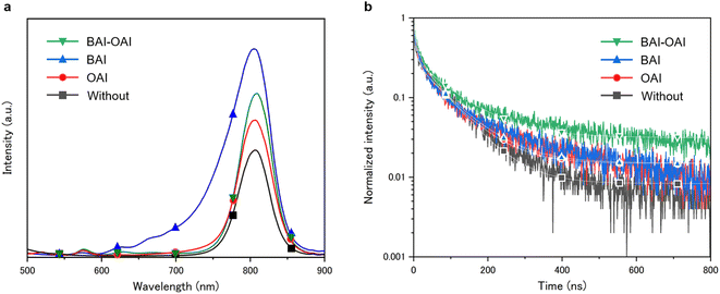 | ||
| Fig. 2 (a) Steady-state photoluminescence (PL) spectra and (b) time-resolved photoluminescence (TRPL) spectra of devices with different passivation materials on the perovskite layer. | ||
Photovoltaic properties, stability, and characterization
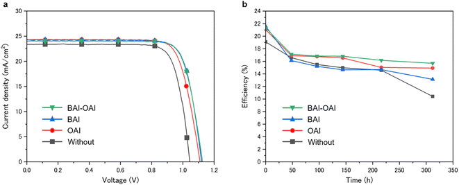
We investigated here the impact of the passivation layer on the device's performance and stability. The performance of fully constructed devices was examined, and the photovoltaic performances and I–V curves are presented in Table 1 and Fig. 3, respectively, for the champion cell with passivation compared to the reference sample. Additional photovoltaic parameters are shown in supplementary Fig. S1–S4.† Power conversion efficiency (PCE) for the BAI-OAI device was 21.6%, whereas the power conversion efficiencies for the BAI, OAI, and non-passivated devices are 21.6, 21.2, and 19.5%, respectively (Fig. 3 and Table 1). Applying the passivation layer raised the open circuit voltage (VOC) from 1.044 V to 1.123 V. The stability data is shown in Fig. 3b. Under 1 sun irradiation (100 mW cm−2, xenon lamp), inert N2, 40% RH, and 30 °C, the stability test was conducted. All devices were encapsulated. The BAI-OAI device had the maximum stability, while the BAI device had the highest power conversion efficiency. As shown in Fig. 3b, it is noteworthy that the BAI-OAI device maintained the highest PCE of 73% from the initial efficiency over 312 hours, as compared to 70% and 60% for the OAI and BAI devices, respectively. The initial PCE significantly decreased from 0 to 48 hours at the beginning. Cation migration may have produced a short performance drop after 50 hours under light irradiation.| J SC (mA cm−2) | V OC (V) | FF | PCE (%) | |
|---|---|---|---|---|
| BAI-OAI | 24.01 | 1.123 | 0.799 | 21.59 |
| BAI | 24.22 | 1.119 | 0.798 | 21.63 |
| OAI | 24.35 | 1.110 | 0.784 | 21.20 |
| Without | 23.39 | 1.044 | 0.797 | 19.48 |
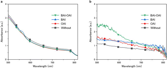
To investigate the effect of the passivation on the stability, we performed light stability tests for the perovskite film under 1 sun irradiation. Images and UV-Vis spectra of the perovskite films are shown in Fig. 4 and 5. As shown in Fig. 4, the devices (BAI-OAI, BAI, OAI, and without passivation) exhibit distinct color changes upon light exposure, which are indicative of perovskite film degradation. By using UV-Vis spectroscopy, this deterioration is verified as shown in Fig. 5. UV-Vis spectra of perovskite films before (Fig. 5a) and after 300 h of light irradiation (Fig. 5b) are shown under varying passivation conditions. Sample configurations are BAI-OAI, BAI, OAI, and without passivation on the perovskite layer/glass substrate. UV-Vis spectroscopy confirms that the absorption transition of the BAI-OAI passivated device was less than under other conditions. These results demonstrate that combining different 2D cations can further suppress photodegradation.
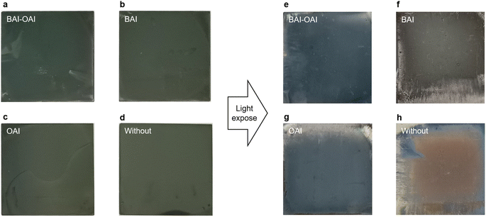 | ||
| Fig. 4 Images of the perovskite films (a–d) before and (e–h) after 300 h of light exposure of the perovskite film. | ||
To verify the effect of the 2D passivation on the 3D perovskite layer, we exposed samples under light irradiation and measured XRD spectra as a function of the time as shown in Fig. 6. Before light irradiation (0 hours), peaks derived from the 2D perovskite were observed below 10° for BAI-OAI, BAI, and OAI samples (Fig. 6a–c). On the other hand, there were no peaks of the 2D perovskite in the case of the sample without passivation at 0 hours. Notably, these 2D perovskite peaks disappeared after 24 hours, which suggests that the 2D perovskite has disappeared during the light irradiation possibly due to the migration of the 2D cation into the 3D perovskite layer. Such a phenomenon is not well known since the 2D perovskite layer was thought to be stable. From this result, we found that the disappearance of the 2D perovskite layer can be the reason for the initial drop in open-circuit voltage and fill factor, resulting in the decrease of the photoconversion efficiency (Fig. 3b and S5–S12 in the ESI†). Furthermore, we measured time-dependent XRD for the samples under dark conditions at room temperature (ESI Fig. S13†) and high temperature (65 °C, Fig. S14, ESI 1†). These results indicate that the 2D perovskite layer can disappear upon exposing it to light or high temperature, which means the 2D perovskite layer on the 3D layer is not stable in either case of BAI-OAI, BAI, or OAI.
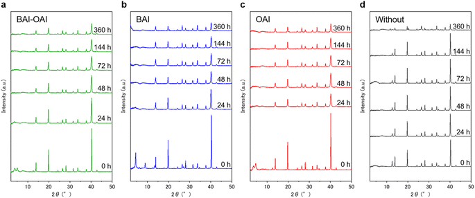 | ||
| Fig. 6 Full XRD spectra of devices with different passivation materials. Devices were irradiated under 1 sun light conditions with (a) BAI-OAI, (b) BAI, and (c) OAI and (d) without passivation. | ||
Fig. 7 shows the XRD spectra in the range of 18.5–21.0° before and after exposure to light for 360 hours. The graphs demonstrate that additional peaks, which were absent before light irradiation, emerged as the δ phase after 360 hours in the cases of BAI, OAI, and without passivation. This δ phase consists of a face-sharing 1D line [PbI6] octahedron, which decreases the photovoltaic parameters.33,34 Notably, the peak intensity of the δ phase with BAI and OAI passivation was lower than that of the sample without passivation. In contrast, no delta-phase peak was observed in BAI-OAI after 360 hours. Interestingly, this finding shows that although the 2D perovskite peaks vanished upon light irradiation, using BAI-OAI for passivation might lessen the production of the delta-phase perovskite (Fig. 6). This result is consistent with the high stability under light exposure by using BAI-OAI passivation (Fig. 3b). To obtain depth profiles of each element, we also assessed glow discharge optical emission spectroscopy (GD-OES) (ESI Fig. S23 and S24†). Irrespective of whether the passivation layer was present on the device or not, there wasn't a noticeable distinction in elemental migration after 160 hours of light irradiation (ESI Fig. S23 and S24†). For the oxygen of the spiro-OMeTAD layer, just a very small rise was seen in both the samples of BAI and without passivation at the perovskite/hole-transport layer interface. The observed variance may have resulted from exposure to dry air during light exposure. The BAI peak was confirmed at the surface of the perovskite layer by the TEM diffraction peak (ESI Fig. S25†). Our findings indicate that the mechanism of the stability enhancement by the 2D/3D perovskite is not due to the 2D perovskite structure itself but the migrated 2D cations in the 3D perovskite layer. Since the peak position of the 3D perovskite (100) was not changed before and after light irradiation (Fig. 6), the migrated 2D cations were not integrated into the 3D perovskite. Possibly, these migrated 2D cations are located at the grain boundary of the 3D perovskite and terminate at the perovskite surface as a passivator, which can be the reason for the improvement of the stability.
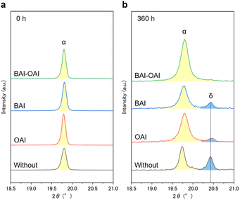 | ||
| Fig. 7 Magnified XRD spectra of each condition (a) before light irradiation and (b) exposed under a solar simulator for 360 hours. | ||
DFT calculation for cation migration
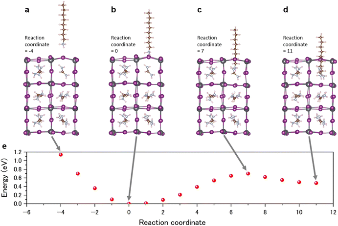
The absorption and subsequent migration of octylammonium (C8H17NH3) (OA) into the perovskite structure was studied using a nudged elastic band calculation based on DFT (Fig. 8). The OA molecule was initially positioned almost vertically outside the perovskite lattice, located approximately 4 Å from the perovskite surface, as depicted in Fig. 8a. The NH3 end, which is denoted as the “head”, is near the perovskite lattice. There is no FA molecule in the perovskite block next to the OA molecule. The molecule's head first adsorbs, then penetrates into the perovskite lattice, and ultimately the head occupies the position of an FA molecule. The OA molecule is most stable when the head adsorbs on the perovskite lattice (Fig. 8b). Penetration into the lattice incurs an energy barrier of approximately 0.6 eV (Fig. 8c). On the other hand, roughly 0.2 eV of the exit barrier is necessary for the OA molecule, with its head at the FA site, to desorb from the perovskite lattice (Fig. 8d). The penetration energy can be overcome by light, and thus the 2D perovskite layer could disappear by penetration of the OA into the FAPbI3 perovskite layer. The penetration and exit barriers are critical quantities on the stability of a passivating molecule; passivating molecules with a large penetration barrier are less likely to migrate into the lattice. Meanwhile, a large exit barrier stabilizes the passivating molecule on the surface and blocks OA molecules from moving out of the lattice. This simulated result can explain the disappearance of the 2D perovskite peak in the XRD spectra (Fig. 6). It was indicated that a larger size cation can be useful to prevent migration. These results describe the stepwise absorption and migration of OA into the perovskite, indicating the role of energy barriers and the potential for light irradiation to facilitate migration.Conclusion
We investigated the effect of 2D passivation on the durability and the dynamics of the 2D perovskite during the stability test by comparing the BAI-OAI, BAI, OAI and without passivation layer. We revealed the impact of cation migration, which is the disappearance of the 2D perovskite passivation layer, by exposure to light and high temperature, resulting in the decrease of the photovoltaic parameters of the perovskite solar cells. Notably, although the 2D perovskite layer disappeared from the 3D perovskite layer upon light irradiation, the solar cells with 2D passivation showed better stability than those without passivation. In particular, the delta phase perovskite, which is harmful to stability, was efficiently reduced by BAI-OAI passivation. Our XRD analysis and DFT calculation showed that the 2D cation could migrate into the 3D perovskite layer by exposure to light and high temperature, which possibly provides the 2D cation with enough energy to overcome the barrier height to migrate into the 3D perovskite layer. Meanwhile, in case of dark conditions, the 2D perovskite can be maintained for a long time. Interestingly, the migrating 2D cation may enhance the stability of the perovskite solar cells rather than the stable 2D perovskite layer itself, since our results show that 2D/3D passivation improves stability. These results suggest that we need to focus more on not only the 2D perovskite layer itself but also the migrated cations and these functions towards further stable perovskite solar cells, which is a new insight on how to approach the 2D/3D passivation system.Experimental
Materials
Methylammonium chloride, cesium iodide, lead iodide, n-butylammonium iodide, n-octylammonium iodide and formamidinium iodide were purchased from TCI. The FTO glass substrate (TEC 10) was purchased from Nippon sheet glass company. Diether and tin(IV) chloride were purchased from Aldrich. Bis(trifluoromethane)sulfonimide lithium salt and the cobalt-complex (FK209) were purchased from Aldrich. DMF, DMSO, isopropanol, and acetonitrile were purchased from Aldrich. The SnO2 nanoparticle dispersed solution was provided by Taki. All chemicals were used as received without further purification.Preparation of characterization samples and solutions
Samples for characterization were prepared starting with a FTO glass or glass substrate. For the XRD samples, the sample structure was FTO/SnO2/perovskite/2D passivation. For the PL samples, the structure was glass/perovskite/2D passivation. For UV-Vis samples, the structure was FTO/SnO2/perovskite/2D passivation. For the GD-OES samples, the structure was FTO/SnO2/perovskite/2D passivation/spiro-OMeTAD/Au. The substrates were treated with UV/O3 for 20 min. Then, a diluted SnO2 dispersed solution was prepared by mixing the SnO2 nanoparticles dispersed solution (S-8) with deionized water in a 1![[thin space (1/6-em)]](https://www.rsc.org/images/entities/char_2009.gif) :
:![[thin space (1/6-em)]](https://www.rsc.org/images/entities/char_2009.gif) 1 volume ratio. 80 μL of the diluted SnO2 dispersed solution was spin coated on the top of the FTO substrate at 3000 rpm for 12 s. These substrates were annealed at 150 °C for 30 min. After cooling down to room temperature, the samples were treated again with UV/O3 for another 20 min. For perovskite deposition, a perovskite precursor composed of three cations, CsFAPbI3, with excess PbI2 was prepared by dissolving 608.3 mg lead iodide, 197.3 mg formamidinium iodide, 17.5 mg cesium iodide and 7.3 mg methylammonium chloride in a 4
1 volume ratio. 80 μL of the diluted SnO2 dispersed solution was spin coated on the top of the FTO substrate at 3000 rpm for 12 s. These substrates were annealed at 150 °C for 30 min. After cooling down to room temperature, the samples were treated again with UV/O3 for another 20 min. For perovskite deposition, a perovskite precursor composed of three cations, CsFAPbI3, with excess PbI2 was prepared by dissolving 608.3 mg lead iodide, 197.3 mg formamidinium iodide, 17.5 mg cesium iodide and 7.3 mg methylammonium chloride in a 4![[thin space (1/6-em)]](https://www.rsc.org/images/entities/char_2009.gif) :
:![[thin space (1/6-em)]](https://www.rsc.org/images/entities/char_2009.gif) 1 volumetric solution of DMSO
1 volumetric solution of DMSO![[thin space (1/6-em)]](https://www.rsc.org/images/entities/char_2009.gif) :
:![[thin space (1/6-em)]](https://www.rsc.org/images/entities/char_2009.gif) DMF. Two step spin-coating was accomplished through a two-step program running at 1000 and 6000 rpm for 12 and 30 s, respectively. At 30 s, in the second step 500 μL of diethyl ether antisolvent was dispensed. After spin coating, the samples were transferred to a 150 °C preheated plate for annealing and left for 10 min to allow optimal crystallization. After bringing the samples down to room temperature, three different isopropanol solutions (0.05 M n-octylammonium iodide for OAI, 0.05 M butylammonium iodide for BAI, and these mixture solutions (1
DMF. Two step spin-coating was accomplished through a two-step program running at 1000 and 6000 rpm for 12 and 30 s, respectively. At 30 s, in the second step 500 μL of diethyl ether antisolvent was dispensed. After spin coating, the samples were transferred to a 150 °C preheated plate for annealing and left for 10 min to allow optimal crystallization. After bringing the samples down to room temperature, three different isopropanol solutions (0.05 M n-octylammonium iodide for OAI, 0.05 M butylammonium iodide for BAI, and these mixture solutions (1![[thin space (1/6-em)]](https://www.rsc.org/images/entities/char_2009.gif) :
:![[thin space (1/6-em)]](https://www.rsc.org/images/entities/char_2009.gif) 1 vol%) for BAI-OAI) were spin-coated directly onto the 3D perovskite for 12 seconds at 4000 rpm in relation to 2D passivation. Then the samples were annealed at 100 °C for 5 min. Following hole-transport layer deposition, spiro-OMeTAD was deposited on the passivated layer by spin-coating (4000 rpm, 12 s). The spiro-OMeTAD precursor solution was prepared by dissolving 100 mg of spiro-OMeTAD in 1279 μL of chlorobenzene, 39 μL of 4-tert-butyl pyridine, 23 μL of bis(trifluoromethane)sulfonimide lithium in acetonitrile solution (517 mg mL−1) and 18 μL of tris(2(1H-pyrazol-1-yl)-4-tert-butylpyridine)cobalt(III) tri[bis(trifluoromethane)sulfonimide] in acetonitrile solution (376 mg mL−1).
1 vol%) for BAI-OAI) were spin-coated directly onto the 3D perovskite for 12 seconds at 4000 rpm in relation to 2D passivation. Then the samples were annealed at 100 °C for 5 min. Following hole-transport layer deposition, spiro-OMeTAD was deposited on the passivated layer by spin-coating (4000 rpm, 12 s). The spiro-OMeTAD precursor solution was prepared by dissolving 100 mg of spiro-OMeTAD in 1279 μL of chlorobenzene, 39 μL of 4-tert-butyl pyridine, 23 μL of bis(trifluoromethane)sulfonimide lithium in acetonitrile solution (517 mg mL−1) and 18 μL of tris(2(1H-pyrazol-1-yl)-4-tert-butylpyridine)cobalt(III) tri[bis(trifluoromethane)sulfonimide] in acetonitrile solution (376 mg mL−1).
Device fabrication
Perovskite solar cell devices were fabricated to obtain performance parameters (JV and stability measurements). After each step, the samples were UV/O3 treated for 20 minutes. The FTO glass was etched by laser. Then, diluted SnO2 dispersed solution was prepared by mixing the SnO2 nanoparticles dispersed solution (S-8) with deionized water in a 1![[thin space (1/6-em)]](https://www.rsc.org/images/entities/char_2009.gif) :
:![[thin space (1/6-em)]](https://www.rsc.org/images/entities/char_2009.gif) 1 volume ratio. 80 μL of the diluted SnO2 dispersed solution was spin coated on the top of the FTO substrate at 3000 rpm for 12 s. These substrates were annealed at 150 °C for 30 min. Thereafter, two step spin-coating of the perovskite precursor was accomplished through a two-step program running at 1000 and 6000 rpm for 12 and 30 s, respectively. At 30 s, in the second step 500 μL of diethyl ether antisolvent was dispensed. The perovskite spin coated precursors were then transferred for annelation at 150 °C for 10 min. Subsequently, OAI, BAI, and OAI-BAI solutions were spin-coated on the perovskite layer at 4000 rpm for 12 s. The samples were then placed on an annealed hotplate at 100 °C for 5 min. Then, the hole transport layer was spin-coated (4000 rpm, 12 s) onto the passivated layer. Finally, a 70 nm gold contact layer was deposited by a thermal evaporation method. The devices were encapsulated.
1 volume ratio. 80 μL of the diluted SnO2 dispersed solution was spin coated on the top of the FTO substrate at 3000 rpm for 12 s. These substrates were annealed at 150 °C for 30 min. Thereafter, two step spin-coating of the perovskite precursor was accomplished through a two-step program running at 1000 and 6000 rpm for 12 and 30 s, respectively. At 30 s, in the second step 500 μL of diethyl ether antisolvent was dispensed. The perovskite spin coated precursors were then transferred for annelation at 150 °C for 10 min. Subsequently, OAI, BAI, and OAI-BAI solutions were spin-coated on the perovskite layer at 4000 rpm for 12 s. The samples were then placed on an annealed hotplate at 100 °C for 5 min. Then, the hole transport layer was spin-coated (4000 rpm, 12 s) onto the passivated layer. Finally, a 70 nm gold contact layer was deposited by a thermal evaporation method. The devices were encapsulated.
Characterization and measurements
The I–V measurements were performed by using a solar simulator, carried out from 1.2 to 0 V and from 0 to 1.2 V as reverse and forward scans, respectively, using a mask of 0.0887 mm2. The scanning step and speed were 10 mV and 100 mV s−1, respectively. Absorption was measured by UV-Vis spectroscopy (JASCO corporation, MSV-5800). SEM images were obtained using a field emission scanning electron microscope (HITACH corporation, SU9000). X-ray diffraction (XRD) analysis was carried out using a D8 Advance diffractometer (Rigaku, SmartLab) with Cu Kα radiation (λ = 1.5418 Å). The elemental depth profile was measured by glow discharge optical emission spectrometry (GD-OES) with a PROFILER2 (HORIBA Ltd) using argon and oxygen sputtering. Samples were subjected to light irradiation using dry air in order to measure GD-OES and UV-Vis. The PL lifetimes were measured using a time-correlated single photon counting system (Fluorolog-QM, Horiba) with excitation at 665 nm. The PL lifetimes were estimated with double exponential fittings. The PL emission was measured with excitation at 420 nm using an FP8600 from JASCO Co. TEM measurement was performed using an ARM200F (JEOL Ltd) with a FIB (Helios600, FEI).Calculations
First-principles calculations based on density functional theory (DFT) in conjunction with the Kohn–Sham scheme35,36 were conducted. The PBE sol functional,37 which is the Perdew–Burke–Ernzerhof functional38 tuned for solids, with spin polarization was used as implemented in the VASP code.39,40 The projector augmented-wave method41 was used with a plane-wave cutoff of 400 eV. The lattice parameters of a perovskite block were a = 6.4075 Å, b = 6.2656 Å, and c = 6.3376 Å based on calculations using PBE sol.42 Rotation of individual molecules was attained using first principles molecular dynamics (MD) simulations, with a fixed number of atoms, volume, and temperature (NVT), of a 2 × 2 × 2 perovskite block supercell at 400 K for 10![[thin space (1/6-em)]](https://www.rsc.org/images/entities/char_2009.gif) 000 steps at 0.5 fs intervals. The resulting structure was then quenched to 0 K. A slab model contains 2 × 2 × 3 perovskite blocks, and the lattice parameters were a = 12.8149 Å, b = 12.5312 Å, and c = 50.7006 Å. The stoichiometry is Pb16I44(FA)12. Charge compensation to account for off-stoichiometry was not conducted. One FA molecule was removed from the “top” layer, and a C8H17NH3 (OA) molecule was inserted into the slab. The nominal charge of this molecule is +1, which is the same as that of FA with +1 nominal charge. Forcing a molecule to have a certain charge was not conducted because DFT finds the electronic state with the lowest total energy of the entire system, and not part of the system. The NH3 end of the molecule was positioned at the center of the perovskite block where the FA molecule was removed. This supercell was relaxed at 0 K and then used as the end state. The OA molecule was shifted by 8 Å and then relaxed to obtain the initial state. A nudged elastic band calculation with 14 intermediate images was conducted.
000 steps at 0.5 fs intervals. The resulting structure was then quenched to 0 K. A slab model contains 2 × 2 × 3 perovskite blocks, and the lattice parameters were a = 12.8149 Å, b = 12.5312 Å, and c = 50.7006 Å. The stoichiometry is Pb16I44(FA)12. Charge compensation to account for off-stoichiometry was not conducted. One FA molecule was removed from the “top” layer, and a C8H17NH3 (OA) molecule was inserted into the slab. The nominal charge of this molecule is +1, which is the same as that of FA with +1 nominal charge. Forcing a molecule to have a certain charge was not conducted because DFT finds the electronic state with the lowest total energy of the entire system, and not part of the system. The NH3 end of the molecule was positioned at the center of the perovskite block where the FA molecule was removed. This supercell was relaxed at 0 K and then used as the end state. The OA molecule was shifted by 8 Å and then relaxed to obtain the initial state. A nudged elastic band calculation with 14 intermediate images was conducted.
Data availability
The data relating to this study have been included as part of the ESI† and are also available from the corresponding authors upon reasonable request.Author contributions
S. M., N. E., and H. K. performed the fundamental experiment, analysis, and writing – original draft, review and editing. N. N. performed photoluminescence spectroscopy, writing, review and editing. Y. H. carried out DFT calculation for chemical structure, writing, review and editing. K. Y. contributed to discussions regarding the thermal test and encapsulation system, and to writing, review and editing. A. K. contributed to GD-OES measurement, writing, review and editing. T. N. M. contributed to supervision, funding acquisition, writing, review and editing. H. K. conceived the idea and was responsible for project administration.Conflicts of interest
There are no conflicts to declare.Acknowledgements
This article is based on results obtained from a project, JPNP21016, commissioned by the New Energy and Industrial Technology Development Organization (NEDO) and Grant-in-Aid for Research Activity Start-up (23K19275) from the Japan Society for the Promotion of Science (JSPS). We thank Sumika Chemical Analysis Service, Ltd for help with TEM measurement.References
- A. Kojima, K. Teshima, Y. Shirai and T. Miyasaka, J. Am. Chem. Soc., 2009, 131, 6050–6051 CrossRef CAS PubMed.
- M. M. Lee, J. Teuscher, T. Miyasaka, T. N. Murakami and H. J. Snaith, Science, 2012, 338, 643–647 CrossRef CAS PubMed.
- A. G. Martin, D. D. Ewan, Y. Masahiro, K. Nikos, B. Karsten, S. Gerald and H. Xiaojing, Prog. Photovolt.: Res. Appl., 2023, 32, 3–13 Search PubMed.
- Y. Zhao, F. Ma, Z. Qu, S. Yu, T. Shen, H. X. Deng, X. Chu, X. Peng, Y. Yuan, X. Zhang and J. You, Science, 2022, 377, 531–534 CrossRef CAS PubMed.
- Best Research-Cell Efficiency Chart, https://www.nrel.gov/pv/cell-efficiency.html.
- F. Ma, Y. Zhao, Z. Qu and J. You, Acc. Mater. Res., 2023, 4, 716–725 CrossRef CAS.
- Q. F. Dong, Y. J. Fang, Y. C. Shao, P. Mulligan, J. Qiu, L. Cao and J. S. Huang, Science, 2015, 347, 967–970 CrossRef CAS.
- S. Dong, A. Valerio, C. Riccardo, Y. Mingjian, A. Erkki, B. Andrei, C. Yin, H. Sjoerd, R. Alexander, K. Khabiboulakh, L. Yaroslav, Z. Xin, A. D. Peter, F. M. Omar, H. S. Edward and M. B. Osman, Science, 2015, 347, 519–522 CrossRef PubMed.
- B. Julian, P. Norman, M. Soo-Jin, H.-B. Robin, G. Peng, K. N. Mohammad and G. Michael, Nature, 2013, 499, 316–319 CrossRef.
- D. S. Samuel, E. E. Giles, G. Giulia, M. Christopher, J. P. A. Marcelo, L. Tomas, M. H. Laura, P. Annamaria and J. S. Henry, Science, 2013, 342, 341–344 CrossRef.
- A. K. Tangra, M. Sharma, U. L. Zainudeen and G. S. Lotey, J. Mater. Sci.: Mater. Electron., 2020, 31, 13657–13666 CrossRef CAS.
- M. B. Thomas, A. E. David, K. Leeor, H. Gary and C. David, Nat. Rev. Mater., 2016, 1, 15007 CrossRef.
- Y. Y. Cho, A. M. Soufiani, J. S. Yun, J. C. Kim, D. S. Lee, J. Seidel, X. F. Deng, M. A. Green, S. J. Huang and A. W. Y. Ho-Baillie, Adv. Energy Mater., 2018, 8, 1703392 CrossRef.
- G. Wu, R. Liang, M. Ge, G. Sun, Y. Zhang and G. Xing, Adv. Mater., 2022, 34, e2105635 CrossRef PubMed.
- Y. Hu, T. Qiu, F. Bai, W. Ruan and S. Zhang, Adv. Energy Mater., 2018, 8, 1703620 CrossRef.
- H. Kim, M. Pei, Y. Lee, A. A. Sutanto, S. Paek, V. I. E. Queloz, A. J. Huckaba, K. T. Cho, H. J. Yun, H. Yang and M. K. Nazeeruddin, Adv. Funct. Mater., 2020, 30, 1910620 CrossRef CAS.
- X. Zhao, T. Liu and Y. L. Loo, Adv. Mater., 2022, 34, e2105849 CrossRef PubMed.
- S. Zouhair, S. M. Yoo, D. Bogachuk, J. P. Herterich, J. Lim, H. Kanda, B. Son, H. J. Yun, U. Würfel, A. Chahboun, M. K. Nazeeruddin, A. Hinsch, L. Wagner and H. Kim, Adv. Energy Mater., 2022, 12, 2200837 CrossRef CAS.
- C. S. Constantinos, H. C. Duyen, J. C. Daniel, Y. Joshua, M. R. James, I. J. Joon, T. H. Joseph and G. K. Mercouri, Chem. Mater., 2016, 28, 2852–2867 CrossRef.
- L. Hyeon-Dong, K. Hobeom, C. Himchan, C. Wonhee, H. Yongseok, K. Young-Hoon, S. Aditya, V. Vijay, K. Joo Sung, C. Jin Woo, L. Chang-Lyoul, K. Dongho, Y. Hoichang, H. F. Richard and L. Tae-Woo, Adv. Funct. Mater., 2019, 29, 1901225 CrossRef.
- M. Lingling, K. Weijun, P. Laurent, W. Yilei, K. Claudine, E. Jacky, R. W. Michael, C. S. Constantinos and G. K. Mercouri, J. Am. Chem. Soc., 2018, 140, 3775–3783 CrossRef.
- X. T. Li, H. Dong, G. Volonakis, C. C. Stoumpos, J. Even, C. Katan, P. J. Guo and M. G. Kanatzidis, Chem. Mater., 2022, 34, 6541–6552 CrossRef CAS.
- Y. Han, S. J. Yue and B. B. Cui, Advanced Science, 2021, 8, e2004805 CrossRef PubMed.
- L. Xiaotong, M. H. Justin and G. K. Mercouri, Chem. Rev., 2021, 121, 2230–2291 CrossRef.
- M. Abuhelaiqa, X. X. Gao, Y. Ding, B. Ding, Z. Yi, M. Sohail, H. Kanda, P. J. Dyson and M. K. Nazeeruddin, Sustainable Energy Fuels, 2022, 6, 2471–2477 RSC.
- H. W. Zhu, S. Teale, M. N. Lintangpradipto, S. Mahesh, B. Chen, M. D. McGehee, E. H. Sargent and O. M. Bakr, Nat. Rev. Mater., 2023, 8, 569–586 CrossRef.
- F. Fiorentino, M. D. Albaqami, I. Poli and A. Petrozza, ACS Appl. Mater. Interfaces, 2022, 14, 34180–34188 CrossRef CAS.
- Y. Hua, Y. P. Zhou, D. C. Hong, S. S. Wang, X. X. Hu, D. Q. Xie and Y. X. Tian, J. Phys. Chem. Lett., 2019, 10, 7025–7030 CrossRef CAS PubMed.
- A. Lemmerer and D. G. Billing, Dalton Trans., 2012, 41, 1146–1157 RSC.
- E. S. Vasileiadou, I. Hadar, M. Kepenekian, J. Even, Q. Tu, C. D. Malliakas, D. Friedrich, I. Spanopoulos, J. M. Hoffman, V. P. Dravid and M. G. Kanatzidis, Chem. Mater., 2021, 33, 5085–5107 CrossRef CAS.
- D. G. Billing and A. Lemmerer, Acta Crystallogr., Sect. B: Struct. Crystallogr. Cryst. Chem., 2007, 63, 735–747 CrossRef CAS PubMed.
- C. W. Mark, S. Michael, D. S. Samuel and A. T. William, ACS Nano, 2016, 10, 7830–7839 CrossRef.
- T. Chen, J. Xie, B. Wen, Q. Yin, R. Lin, S. Zhu and P. Gao, Nat. Commun., 2023, 14, 6125 CrossRef CAS PubMed.
- P. Gratia, I. Zimmermann, P. Schouwink, J. H. Yum, J. N. Audinot, K. Sivula, T. Wirtz and M. K. Nazeeruddin, ACS Energy Lett., 2017, 2, 2686–2693 CrossRef CAS.
- P. Hohenberg and W. Kohn, Phys. Rev., 1964, 136, B864–B871 CrossRef.
- W. Kohn and L. J. Sham, Phys. Rev., 1965, 140, A1133–A1138 CrossRef.
- J. P. Perdew, A. Ruzsinszky, G. I. Csonka, O. A. Vydrov, G. E. Scuseria, L. A. Constantin, X. Zhou and K. Burke, Phys. Rev. Lett., 2008, 100, 136406 CrossRef.
- J. P. Perdew, K. Burke and M. Ernzerhof, Phys. Rev. Lett., 1996, 77, 3865–3868 CrossRef CAS PubMed.
- G. Kresse and J. Furthmüller, Phys. Rev. B, 1996, 54, 11169–11186 CrossRef CAS.
- G. Kresse and D. Joubert, Phys. Rev. B, 1999, 59, 1758–1775 CrossRef CAS.
- P. E. Blöchl, Phys. Rev. B, 1994, 50, 17953–17979 CrossRef.
- B. Federico, B. W. Alison and W. Aron, APL Mater., 2013, 1, 042111 CrossRef.
Footnotes |
| † Electronic supplementary information (ESI) available. See DOI: https://doi.org/10.1039/d4se01227e |
| ‡ These authors contributed equally. |
| This journal is © The Royal Society of Chemistry 2025 |

