Diameter dependent performance of silicon nanowire anodes grown on 3D current collectors for lithium-ion batteries†
Mei
Li
,
Niraj Nitish
Patil
 ,
Shalini
Singh
 ,
David
McNulty
 * and
Kevin M.
Ryan
*
Department of Chemical Sciences and Bernal Institute, University of Limerick, Limerick, V94 T9PX, Ireland. E-mail: david.mcnulty@ul.ie
First published on 28th November 2024
Abstract
Si nanowires (Si NWs) with diameters tuned from ∼35 to 100 nm were directly grown on large-area (30 cm2) stainless-steel mesh (SSM) substrates via a facile vapour–liquid–solid approach. The 3-dimensional open mesh and interwoven structure of SSM allow for the dense growth of well-anchored Si NWs and a sufficient buffer space for repeating volume changes during electrochemical cycling. In this study, the controlled synthesis of silicon nanowires with different diameters and the influence of nanowire diameter on electrochemical performance were investigated for the first time. We demonstrate that the diameter of Si NWs has a significant influence on their electrochemical performance as anode materials for lithium-ion batteries. Through systematic electrochemical testing, we observed that rate capability, specific capacities and capacity retention obtained for Si NWs samples are inversely proportional to nanowire diameter, demonstrating a diameter-dependent performance of silicon nanowires anodes. Si NWs with an average size of 100 nm exhibited specific capacities of ∼800 mA h g−1. Reducing the diameters to 55 nm gave ∼1200 mA h g−1 whereas Si NWs with an average diameter of ∼35 nm demonstrated a specific capacity of ∼1500 mA h g−1 when cycled with an applied specific current of 1 A g−1. The phase transition and structure evolution of Si NWs before and after cycling were investigated by Raman spectroscopy and electron microscopy.
Introduction
Developing high-capacity anodes for rechargeable lithium-ion (Li-ion) batteries is essential to enhance the energy density of next-generation Li-ion batteries to be compatible with future applications and meet soaring energy storage needs.1–3 Silicon (Si) is a promising anode material for Li-ion batteries as it is an abundant material with a high theoretical specific capacity (3579 mA h g−1 for Si in Li15Si4), which is nearly 10 times higher than graphite (372 mA h g−1 for C in LiC6), and the compatible redox potential of Si (0.4 V vs. Li/Li+) offers a wide range of possibilities toward various storage devices.4–6 However, the significant volumetric expansion of Si anodes during alloying with lithium-ions (Li+) can result in severe material pulverization and repeated solid electrolyte interphase (SEI) fracture/reform. These issues cause active material to be disconnected from current collectors (CCs), leading to irreversible capacity loss and a relatively short lifetime.7–9 One approach for enhancing the electrochemical performance of Si-based anodes is to use directly grown nanostructured Si on 3D CCs instead of planar electrodes to mitigate the volume change effect and improve their cyclability.10–13Silicon nanowires (Si NWs) have advantages over nanoparticles,14–17 and nanotubes,18–20 as NWs have facial strain relaxation to better accommodate volume expansion, an efficient axial charge transfer pathway, and shorter radial Li+ diffusion distances due to their one-dimensional (1D) character.21–23 In addition, computation results of the stresses in NWs during lithiation have shown that surface tension can induce compressive stress, which inhibits crack propagation and could extend cycle life for small NWs.24 The size effect in Si anodes and its correlation to volume changes has also been studied in nanoparticles however this has not been extended significantly to nanowires.17,25,26 Interestingly a critical size of the Si nanoparticles (Si NPs) was determined at ∼150 nm, where cracking or fracturing after lithiation-induced swelling and surface stress is reduced.15 As NWs will be greater than 150 nm in the longitudinal direction a study on diameter dependent effects correlated to wire diameter is important.
The structure of the electrode is also relevant with the direct growth of wires on a 3D current collector allowing analysis of diameter effects independent of other factors for example in slurries where binders and conductive additives are present. A CC for directly grown wires needs to be mechanically stable, facilitate electronic transport and ideally provide high surface area for improving electrochemical performance.27–29 Alloying mode materials with nanowire morphologies have been grown on different CC substrates including Cu foils,27,28 stainless-steel foils,30–33 titanium foils,34 stainless-steel cloth,10 and carbon fibre cloth.35,36 Here we use stainless-steel mesh (SSM) with a 3-dimensional (3D) open structure as it provides high surface area, good conductivity and sufficient buffer space for volume changes, and also enables a thorough characterisation of Si NWs after cycling without other contaminations.
The synthesis approaches of Si NWs include top-down (e.g. etching bulk silicon with HF) and bottom-up methods (such as seeded protocols using silane in CVD, supercritical fluid or wet chemical processes).8,31,37,38 A solvent-vapor-growth (SVG) approach has previously been developed by our group, which is capable of growing Si NWs from a safer liquid precursor under an ambient atmosphere.10,12,13,27,28,39–41 It is worth noting that the required growth conditions and the quality of the Si NWs vary based on 3 types of metal catalysts (type-A, type-B, and type-C) according to their metal–Si binary phase.37,38,41 The eutectic point of type-A metal gold is located at a Si composition of >10 atom% Si and is known to contaminate Si NWs.37,38 Type-B catalyst Sn can accommodate 1 atom% Si with potential diameter control, while type-C transition metal forms a silicide alloy.27–29,42,43
In this study, Si NWs with four different average diameters were synthesized on relatively large pieces of SSM (5.0 × 6.0 cm) via a VLS approach. The average diameters of the NW samples were ∼35 nm, 55 nm, 85 nm and 100 nm, and these samples are henceforth referred to as Si35, Si55, Si85, and Si100, respectively. It was found that the diameter of Si NWs plays a key role in the phase transition and morphological evolution during initial electrochemical cycling, which impacts the rate capability and stability. Electron microscopy, X-ray diffraction, X-ray photon spectroscopy, and Raman spectroscopy were used to systematically unravel the size correlation, chemical composition, and structure evolutions of Si NWs with different diameters. An inverse relation between electrochemical performance and wire diameter is observed with the smallest diameter wires showing the best rate capability at higher current density and extended cycles.
Results and discussion
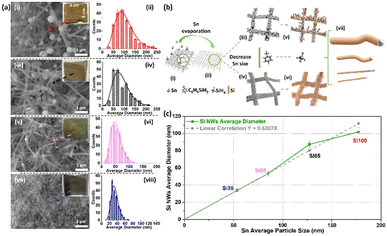
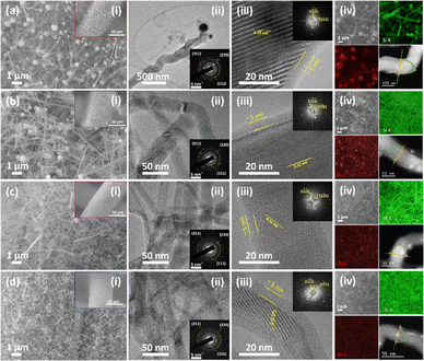
Scanning electron microscopy (SEM) images, size distribution histograms, and optical images of Si NWs after the synthesis reaction are shown in Fig. 1a. Sn was deposited in four different thicknesses 10, 20, 50 and 100 nm, (corresponding SEM images and average sizes of Sn seeds are shown in Fig. S1†) leading to wires of ∼35 nm, ∼55 nm, ∼85 nm and ∼100 nm respectively. Larger initial Sn particle sizes (histograms in Fig. S1†) resulted in the growth of Si NWs with larger diameters (histograms in Fig. 1a). All samples exhibit dense growth with good coverage of Si NWs on the SSM substrates with Si100 showing a dark brown colour, Si85 light brown, Si55 grey-green colour and Si35 dark grey in insets. A schematic of the VLS process is shown in Fig. 1b. The 3D mesh structure bare SSM provides electric conductivity and high surface area for hosting Sn catalysts with different sizes. The Sn catalyst melts as droplets on the SSM during the reaction, and the silane (SiH4, vapour) in situ decomposed from PS and absorbed into the Sn droplets. Excess Si crystallises from the saturated droplets as Si NWs (solid) with diameters deriving from the droplet size and solubility of Si in the alloy.31,37,38 The average diameter of Si NWs increases with the size of the evaporated Sn particles as shown in Fig. 1c. The correlation differs slightly for the larger Sn size >100 nm, which may be due to the Sn island formation with a broader distribution in Fig. S1a–b,† resulting in a wide range size of Sn–Si droplets when the reaction temperature reached the melting point of Sn. The nature of the low eutectic point and low surface tension of type B catalyst Sn are the key factors in defining the extracted diameter of Si NWs in good agreement with previous studies.12,13,38SEM, TEM images, and energy-dispersive X-ray spectroscopy (EDX) elemental mapping with line scan spectra of the Si NWs are presented in Fig. 2. The high coverage of Si NWs can be observed with NW growth extending over all SSM substrates in Fig. 2a–d(i), for comparison, SEM images of bare SSM are shown in Fig. S2.† TEM images of Fig. 2a–d(ii)–(iii) reveal lattice features of a crystalline Si (c-Si) core covered by a ∼5 nm thick amorphous Si (a-Si) layer and a lattice spacing of ∼0.31 nm. The selected area electron diffraction (SAED) and fast Fourier transform (FFT) pattern as insets showed a pure Si phase, indicated by the presence of (111), (220), and (311) lattice planes, which is consistent with the X-ray diffraction (XRD) results (Fig. 3a) and previous reports.10,44 Associated scanning transmission electron microscopy (STEM), energy-dispersive X-ray (EDX) spectroscopy elemental mapping and line scan spectra are shown in Fig. 2a–d(iv) and S3† from dark-field STEM (DF-STEM). EDX mapping images demonstrate the well-distributed Sn seeds and densely grown Si NWs with different diameters. There is a sharp increase in the Si signal that occurs simultaneously with the O and C signal from the edge of a NW and the intense Si signal remained in the core without any O and C in the line scan spectra, demonstrating that the surface may contain O and C from the decomposition of precursor and the crystal core is pure Si.
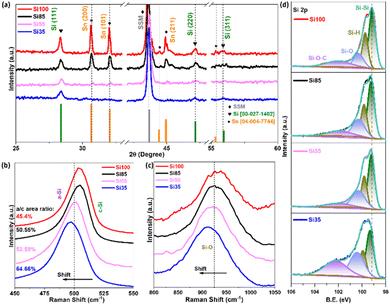
The X-ray diffraction (XRD) patterns of all Si NWs samples containing characteristic peaks agreed with Si (JCPDS no.: 00-027-1402) and Sn (JCPDS no.: 04-004-7744) are shown in Fig. 3. Major peaks at 28.37°, 47.15°, and 55.89° can be indexed to crystal Si (111), Si (220), and Si (311), respectively.10,41,45 Peaks arising at 30.70°, 32.04°, and 44.97° are from Sn (200), Sn (101) of crystalline β-Sn structure, and Sn (211) with a broader α-Sn peak, while the sharp peak at 43.70° is from the underlying SSM substrate agreed with previous reports.10,41,45 More details of chemical and phase composition were revealed by Raman spectra covering Si–Si, Si–O in Fig. 3b–c and S4–S5† (D and G bands from C, full range Raman spectra and deconvoluted peaks from Si–Si spectra). The proposed a-Si surface was confirmed in Fig. 3b with broad Si–Si peaks at ∼500 cm−1, originated from a-Si appearing at ∼480 cm−1 and c-Si allocated at ∼503 cm−1 after deconvoluted Si–Si spectra in Fig. S5.†46,47 Note that the full width at half maximum (FWHM) of Si–Si peak becomes broader from 19.49 cm−1 of Si100 to 25.26 cm−1 of Si35 in Table S1,† and the band position shifts toward lower wavenumbers which may be attributed to the smaller c-Si diameter.46,47 An increased amorphous to crystalline peak (a/c) area ratio of 45.40%, 50.55%, and 52.59% to 64.66% in Fig. S5† further indicates the decreasing c-Si sizes as the scattering of a-Si became more intense over the crystalline core.47 The vibrations at ∼925 cm−1 are from Si–O (Fig. 3c) showing a slight decrease in wavenumber, this could be due to the surface of Si NWs being oxidized after reaction.46 The two peaks at 1334 cm−1 and 1595 cm−1 for all four samples in Fig. S4a† are ascribed to the carbon D and G bands and are characteristic of a carbon coating caused by the decomposition of phenyl group at a reaction temperature of 460 °C.35,48 Calculated ID/IG ratios indicate that the carbon coating was highly disordered as an amorphous phase.41,49 This is consistent with XRD results where only c-Si was preserved without any formation of SiC in Fig. 3a, and the element line scan profile in Fig. 2a–d(iv) with the trace carbon on the surface. The chemical composition of the natively formed amorphous layer was further analysed by X-ray photoelectron spectroscopy (XPS). Four peaks could be derived from the Si 2p spectrum (Fig. 3d) with different diameters. The binding energy of 99.0 eV arises from the zero-valent Si and 100.2 eV comes from the SiOx, while 99.8 eV originated from organosilicon and a broad shoulder peak at ∼102 eV of siloxane from precursor decomposition.41,49 By comparison, the intensity of the intrinsic Si is stronger than that of SiOx and organosilicon, indicating a thin oxide layer on the Si surface as shown in the TEM images. The decreased intensity and shifting of Si–Si along with increasing Si–O in Fig. 3b–d as the diameter gets smaller reveals a higher O content on the surface, which corresponds to the element line scan profiles in Fig. 2. Fig. S6† presents the C 1s and O 1s spectra of all electrodes, the peaks arising at 284.8 (C–C/C![[double bond, length as m-dash]](https://www.rsc.org/images/entities/char_e001.gif) C), 285.9 (C–O), and 291.4 eV (–CO3) are contributions from adventitious carbon or hydrocarbons left from the precursor decomposition.41,49 Finally, the O 1s peak is originated from O (−2) at 532 eV and siloxane at the binding energy around 533 eV.49 A correlation of results from XRD, Raman spectroscopy and XPS spectra indicates that the main product of all reactions was pure Si with minor amounts of carbon and oxygen present due to the decomposition of the precursor.
C), 285.9 (C–O), and 291.4 eV (–CO3) are contributions from adventitious carbon or hydrocarbons left from the precursor decomposition.41,49 Finally, the O 1s peak is originated from O (−2) at 532 eV and siloxane at the binding energy around 533 eV.49 A correlation of results from XRD, Raman spectroscopy and XPS spectra indicates that the main product of all reactions was pure Si with minor amounts of carbon and oxygen present due to the decomposition of the precursor.
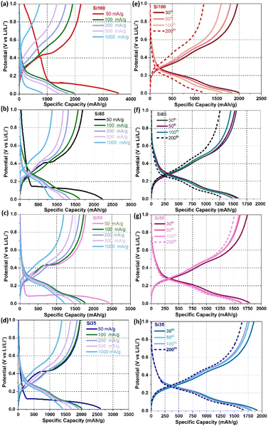
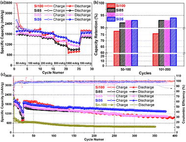
To investigate the effect on the electrochemical performance of Si NWs grown directly on the SSM with different diameters, all electrodes were assembled into half-cells with Li foil as the counter electrode. Si NW samples were cycled on the growth substrate without additional binders or conductive additives. The voltage–capacity profiles from galvanostatic cycling in Fig. 4a–d revealed electrochemical reactions that occur in different applied current densities from 50 to 1000 mA g−1. The long plateaus in the initial cycle at an applied specific current of 50 mA g−1 originate from the lithiation of c-Si to a-Si at ∼0.1 V, and further lithiated to amorphous Li15Si4 alloy at the slopes below 0.1 V during the first lithiation in Fig. S7.†17,23,50 Features in the voltage–capacity profiles for the initial lithiation that occurs at potentials >0.4 V are typically related to the formation of a solid electrolyte interphase (SEI) layer.7,23,50 Si100 with the largest diameter exhibited a significant loss of reversible capacity on the first cycle in Fig. S7† and cycles at a higher applied current density of 50 and 1000 mA g−1 in Fig. 4a–d compared to other samples. The long flat plateaus of Si100, Si85, Si55, and Si35 delivered initial lithiation capacity of 3553, 2217, 2409, 2601 mA h g−1 with the corresponding initial coulombic efficiencies (ICE) of 62%, 76%, 74%, 75%, respectively. The low ICE of Si100 may be due to the volume expansion and structure fracture on the first lithiation compared to the Si NWs that are <100 nm.17,51 Meanwhile, the rapidly decaying capacity during the rate capability test of Si100 in Fig. 4a indicated that they are not as stable as the smaller NWs at a higher current density of 1000 mA g−1 due to the structure fracture, which will be discussed more in detail in the post-cycling characterizations.
The cyclability of Si85, Si55, and Si35 maintained well with the reversible capacity decreases <20% from the 30th to 200th cycles, where Si100 has a capacity loss of 40% with a rapid decline in the capacity after 50 cycles in Fig. 4e–h. Although Si100 show higher capacity on the first cycle, they are prone to significant reversible capacity loss at higher current densities and prolonged cycling. Additional analysis (differential charge curves) and electrochemical tests (rate tests and cyclic voltammetry) were performed to further investigate the influence of Si NW diameter on their electrochemical performance.
The differential charge (dQ/dV) and cyclic voltammetry (CV) curves of the 1st, 2nd, and 5th cycle of all Si NW samples are demonstrated in Fig. 5. During the first lithiation, the cathodic peak at ∼630 mV is from the lithiation of Sn seeds, and SEI formation at ∼420 mV (step I in Fig. 5a and e), but the contribution from Sn and the reformation of SEI (Fig. 5b–d and f–h) are negligible due to the smaller size and less amount of Sn seeds in the Si NWs that are <100 nm.10,52,53 The characteristic sharp cathodic peak at <150 mV with a broad shoulder peak <100 mV (step II) that appeared in all samples is associated with the phases transformation from c-Si to a-Si and the coexistence of two phases of a-Si and lithiated amorphous LixSi (a-LixSi), which are agreed with the previously reported Si NWs.17,41,44,45 The reduction corresponds to the initial alloying of crystalline silicon is observed in the differential charge plots for the first lithiation and is not observed in subsequent cycles. Its absence in subsequent cycles, suggests that after the initial lithiation the Si does not return to its initial crystalline state and instead cycles reversibly as amorphous silicon.
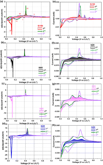 | ||
| Fig. 5 (a–d) Differential charge curves, and (e–h) CV curves of (red) Si100, (black) Si85, (pink) Si55, and (blue) Si35 at 0.1 mV s−1 scan rate from 0.01–1.0 V. | ||
Note that the shifting toward the lower potential of the sharp peak and smaller shoulder peaks below 100 mV were observed and could be attributed to the amorphization of smaller c-Si and further lithiation of a-LixSi in the NWs that are <80 nm.15,24,44,54 During the first delithiation, all samples displayed one broad peak at 320 mV (step III) and a pronounced anodic peak at ∼430 mV (step IV), revealing the coexistence of two phases of a-LixSi and Li15Si4.17,45,46 Small peaks at >580 mV are the delithiation of Li7Sn2 (step V) corresponding to the peaks observed from the pure Sn electrode (voltage profiles and dQ/dV curves in Fig. S8†).52 In the following scans, the bell-like cathodic peaks at 220 mV and 100 mV correspond to the formation of a-Li15Si4 (step VI).41,44,45 The majority of c-Si is converted into a-LixSi phase after the first cycle as the sharp cathodic peak disappeared while two bell-shaped peaks remained for the following cycles. Reoccurring pronounced anodic peak at 430 mV in the 5th cycle (purple curve) of Si55 and Si35 in Fig. 5c and d indicated that smaller Si NWs were able to fully delithiated from a-LixSi to Li15Si4, while less Li+ were extracted from the Si NWs that >80 nm with bell-like peaks.17,55 The areas of the cathodic and anodic peaks in the CV curves shown in Fig. 5e–h increased as the cycle number increases (20 cycles in Fig. S9†), implying an increased in the charge stored during these processes, due to the activated Si in the first few cycles under a fast scan rate of 0.1 mV s−1.10,55 Results from dQ/dV analysis and CV tests suggest that Si NWs with diameters <80 nm can be fully lithiated and delithiated during the initial cycles at the applied specific current that was used.
Galvanostatic cycling was carried out to further analyse the rate capability (from 50 mA g−1 to 1000 mA g−1) and cyclability of all samples with prolonged cycles. The rate performance is enhanced by reducing diameters as Si55 and Si35 show better rate capacities with 90% retaining capacities of the initial capacity, delivering 1262 mA h g−1 and 1495 mA h g−1, compared to the 824 mA h g−1 and 972 mA h g−1 of Si100 and Si85 at 1000 mA g−1 in Fig. 6a. For comparison, Si microparticles (Si MPs) without an amorphous surface layer were cycled under the same conditions. A rapid capacity decay below 100 mA h g−1 of Si MPs was observed when cycled at 1000 mA g−1 in Fig. S10a.† These results demonstrate the impressive rate capability of Si NWs that are 35 nm and further demonstrate the diameter-dependent electrochemical performance of Si NWs anodes. Additional synthesis of Si NWs and electrochemical tests were performed with Si NWs grown on stainless-steel fibre cloth (SSFC) and planar stainless-steel sheet (SSS) (SEM images shown in Fig. S11†) to further demonstrate the advantages of using SSM as an electrically conductive substrate. The Si35 sample grown on SSM yields a high reversible capacity of 1623 mA h g−1 compared to 1121 mA h g−1 of Si NWs/FFSC and 1086 mA h g−1 of Si NWs/SSS after 100 cycles at 100 mA g−1 (Fig. S10b†). The specific capacities obtained with Si35 samples in this study are greater than or comparable to previously reported values for Si NWs with/without surface layer grown on carbon fibre,56 copper foam,57 SSFC,10 and SSS12 in Table S2.† Previous reports which have relied on the addition of CNTs and other carbons to achieve the specific capacities which we have obtained without any carbon additives or binders. These results demonstrate that the strongly anchored Si NWs on the SSM facilitated the electron transfer and avoiding the loss of electric connection.
The cyclability of Si NWs with diameters ranging from 100 nm to 35 nm was further examined by galvanostatic cycling. Si NWs with smaller diameters maintained capacity retention above 90%, while the Si100 obtained the lowest reversible capacity retention of 76% at 100 mA g−1 for 200 cycles in Fig. 6b. This suggests that the loss of reversible capacity may be due to the larger diameters of Si100.17 For the galvanostatic cycling in Fig. 6c, the specific capacities of Si35 surpassed Si100 after 100 cycles, which could be attributed to the smaller diameters alleviating volume expansions.15 It is worth noting that the highest specific capacity values were obtained with the smallest diameter Si NWs (Si35), which demonstrated the slowest capacity decay with a capacity retention of 84% from 50 to 350 cycles. Pure Sn-100 electrodes with the same average Sn size and loading of Si100 electrodes were synthesized and tested as a control sample, where a reversible capacity of 534 mA h g−1 and 79% capacity retention were obtained after 100 cycles.52,53 Furthermore, Si35 offer advantages in terms of higher specific capacity and capacity retentions over recently published results as listed in Table S2.† The improvement of rate capability, capacity retention and cyclability from the Si35 could be attributed to the smaller diameter, which mitigated the volume expansion, and avoided the loss of reversible capacity. Additional post-cycling characterizations were performed and are discussed in the following section.
Postmortem Raman spectroscopy and SEM and TEM imaging were performed to investigate the influence of electrochemical cycling on the Si phase and morphology of all four different diameter Si NWs. The c-Si was lithiated into the a-Si phase after the first cycle based on the characteristic peak shape changes in the dQ/dV and CV curves in Fig. 5, where Raman spectra of the Si NWs after 5 cycles in Fig. 7a–d and S12† (full range Raman spectra) confirmed this phase transformation. The FWHMs of Si–Si pronounced peaks from all cycled samples were increased by 5–13 cm−1 in Table S1† and shifted towards lower frequency after 5 cycles due to the amorphization of Si, and the intensity of a-Si at ∼480 cm−1 has increased and dominated in the Si35 sample in Fig. 7d.47 This demonstrated that the smaller wires have likely become completely amorphous after the initial cycles while partial lithiated Si NWs >80 nm remained in the crystalline phase. The morphology evolution of the cycled Si NWs electrodes was investigated by SEM and TEM imaging after delithiation from the 5th to 20th cycles in Fig. 7e–p. Some expanded wires from Si100 and Si85 started to fracture and detach from the SSM, while Si55 and Si35 were densely anchored and formed interconnected porous structures after 5 cycles in Fig. 7e–h and 10 cycles in the SEM images shown in Fig. S13.† TEM images of all pristine Si NWs samples have shown in Fig. 7i–l (left) with crystalline nanowire structure as comparison to the post-cycling morphology (right). Previous studies of Si NWs have suggested that the lithiation initiated at the surface and the lithium diffused into the crystal core forming the amorphous network structure.10,13,51,58 The Si35 started forming a network structure after 5 cycles in Fig. 7l, while an expanded wire structure can be observed in other Si NWs that are larger than 50 nm.59
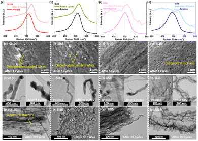 | ||
| Fig. 7 (a–d) Raman spectrum of Si–Si peak, (e–h) SEM and (i–l) TEM images of pristine Si NWs (left) and Si NWs after 5 cycles (right), (m–p) TEM images after 20 cycles of Si100, Si85, Si55, and Si35. | ||
Once delithiated after 20 cycles, all nanowires in Fig. 7i–l showed the complete amorphous network structures after fully lithiated, which has been demonstrated in previous studies from our group.10,12,32,40 This network structure is highly porous and could provide sufficient buffer space to accommodate the volume changes of Li+ alloying and dealloying without further cracks. This further demonstrated that the cycled Si NWs remained in good contact with SSM because of the intertwined network formation, which can form in the early cycles when reduce the diameter of Si NWs. Our results indicate that the electrochemical performance of Si NWs is diameter-dependent with the best performance from the Si NWs with an average diameter of 35 nm, where the full lithiation of Si and the porous network formation can be achieved upon early cycles, enhancing the cyclability of Si NWs anodes.
Conclusions
In conclusion, we have demonstrated a tunable synthesis procedure to prepare Si NWs with diameters ranging from ∼35 to 100 nm. The effects of Si NWs' diameter on the phase transition, and structural evolution during electrochemical cycling have been revealed and discussed. Si NWs anodes with an average diameter of 35 nm delivered the highest reversible capacity of 1380 mA h g−1 at 100 mA g−1 after 350 cycles, and demonstrated impressive rate capability that can sustain high current density up to 1000 mA g−1 with 1495 mA h g−1 and retain 92% of its reversible capacity after returning to 100 mA g−1. Meanwhile, a capacity retention of 88% and an average coulombic efficiency of 98% were achieved over 350 cycles. The ex situ electron microscopy and Raman analysis of the Si NWs anodes after the 5th, 10th, and 20th cycle showed Si35 exhibited a fully lithiated amorphous phase with a mechanically stable porous network structure at the 5th cycle whereas the larger Si NWs after 20 cycles. A correlation of results from structural and electrochemical characterisation indicates that the improved rate capability, specific capacity, and capacity retention obtained for Si35 can be attributed to their smaller diameters. Additionally, we believe that this work offers an understanding of the critical dimensions of silicon nanowires and contributes to the development of alloying anodes for Li-ion batteries.Data availability
The data that support the findings of this article have been included as part of the ESI.† All data are available from the corresponding author upon reasonable request.Author contributions
Mei Li: conceptualization, investigation, characterization, methodology, writing – original draft. Niraj Nitish Patil: Raman spectra analysis. Shalini Singh: writing – review & editing. David McNulty: conceptualization, investigation, writing – review & editing. Kevin M. Ryan: writing – review & editing, funding acquisition, project administration.Conflicts of interest
There are no conflicts to declare.Acknowledgements
M. L. acknowledges Science Foundation Ireland (SFI), CONFIRM smart manufacturing centre, and Bernal Institute. This publication has emanated from research conducted with the financial support of Johnson & Johnson and Confirm Centre for Smart Manufacturing under Science Foundation Ireland Grant number 16/RC/3918. D. M. N. acknowledges that this publication has emanated from research conducted with the financial support of Science Foundation Ireland and the Irish Research Council under grant number 21/PATH-S/9717. S. S. and N. P. acknowledges that this publication has emanated from research conducted with the financial support of Science Foundation Ireland under grant number 22/FFP-P/11591 and 12/rc/2278_p2.Notes and references
- G. G. Eshetu, H. Zhang, X. Judez, H. Adenusi, M. Armand, S. Passerini and E. Figgemeier, Nat. Commun., 2021, 12, 5459 CrossRef CAS.
- G. Zhu, D. Chao, W. Xu, M. Wu and H. Zhang, ACS Nano, 2021, 15, 15567–15593 CrossRef CAS.
- D. McNulty, A. Hennessy, M. Li, E. Armstrong and K. M. Ryan, J. Power Sources, 2022, 545, 231943 CrossRef CAS.
- M. Je, D. Y. Han, J. Ryu and S. Park, Acc. Chem. Res., 2023, 56, 2213–2224 CrossRef CAS.
- Z. Zhao, F. Chen, J. Han, D. Kong, S. Pan, J. Xiao, S. Wu and Q. Yang, Adv. Energy Mater., 2023, 13, 2300367 CrossRef CAS.
- Y. Li, Q. Li, J. Chai, Y. Wang, J. Du, Z. Chen, Y. Rui, L. Jiang and B. Tang, ACS Mater. Lett., 2023, 5, 2948–2970 CrossRef CAS.
- Y. He, L. Jiang, T. Chen, Y. Xu, H. Jia, R. Yi, D. Xue, M. Song, A. Genc, C. Bouchet-Marquis, L. Pullan, T. Tessner, J. Yoo, X. Li, J. G. Zhang, S. Zhang and C. Wang, Nat. Nanotechnol., 2021, 16, 1113–1120 CrossRef CAS PubMed.
- H. Li, H. Li, Y. Lai, Z. Yang, Q. Yang, Y. Liu, Z. Zheng, Y. Liu, Y. Sun, B. Zhong, Z. Wu and X. Guo, Adv. Energy Mater., 2022, 12, 2102181 CrossRef CAS.
- J. P. Pender, G. Jha, D. H. Youn, J. M. Ziegler, I. Andoni, E. J. Choi, A. Heller, B. S. Dunn, P. S. Weiss, R. M. Penner and C. B. Mullins, ACS Nano, 2020, 14, 1243–1295 CrossRef CAS PubMed.
- S. Imtiaz, I. S. Amiinu, D. Storan, N. Kapuria, H. Geaney, T. Kennedy and K. M. Ryan, Adv. Mater., 2021, 33, 2105917 CrossRef CAS PubMed.
- K. Stokes, W. Boonen, H. Geaney, T. Kennedy, D. Borsa and K. M. Ryan, ACS Appl. Mater. Interfaces, 2019, 11, 19372–19380 CrossRef CAS.
- T. Kennedy, M. Bezuidenhout, K. Palaniappan, K. Stokes, M. Brandon and K. M. Ryan, ACS Nano, 2015, 9, 7456–7465 CrossRef CAS.
- K. Stokes, H. Geaney, G. Flynn, M. Sheehan, T. Kennedy and K. M. Ryan, ACS Nano, 2017, 11, 10088–10096 CrossRef CAS PubMed.
- H. Wang, X. Cao, H. Gu, Y. Liu, Y. Li, Z. Zhang, W. Huang, H. Wang, J. Wang, W. Xu, J.-G. Zhang and Y. Cui, ACS Nano, 2020, 14, 4601–4608 CrossRef CAS PubMed.
- X. H. Liu, L. Zhong, S. Huang, S. X. Mao, T. Zhu and J. Y. Huang, ACS Nano, 2012, 6, 1522–1531 CrossRef CAS PubMed.
- J. Zhu, T. Wang, F. Fan, L. Mei and B. Lu, ACS Nano, 2016, 10, 8243–8251 CrossRef CAS PubMed.
- F. Wu, Y. Dong, Y. Su, C. Wei, T. Chen, W. Yan, S. Ma, L. Ma, B. Wang, L. Chen, Q. Huang, D. Cao, Y. Lu, M. Wang, L. Wang, G. Tan, J. Wang and N. Li, Small, 2023, 19, 2301301 CrossRef CAS PubMed.
- F. Wang, P. Li, W. Li and D. Wang, ACS Nano, 2021, 16, 7689–7700 CrossRef PubMed.
- C. P. Fucetola, J. T. Wang, O. A. Bolonduro, C. M. Lieber and B. P. Timko, ACS Nano, 2024, 18, 3775–3782 CrossRef CAS.
- M.-H. Park, M. G. Kim, J. Joo, K. Kim, J. Kim, S. Ahn, Y. Cui and J. Cho, Nano Lett., 2009, 9, 3844–3847 CrossRef CAS.
- S. Karuppiah, C. Keller, P. Kumar, P. H. Jouneau, D. Aldakov, J. B. Ducros, G. Lapertot, P. Chenevier and C. Haon, ACS Nano, 2020, 14, 12006–12015 CrossRef CAS.
- S. A. Ahad, T. Kennedy and H. Geaney, ACS Energy Lett., 2024, 1548–1561 CrossRef CAS PubMed.
- C. K. Chan, H. Peng, G. Liu, K. McIlwrath, X. F. Zhang, R. A. Huggins and Y. Cui, Nat. Nanotechnol., 2008, 3, 31–35 CrossRef CAS PubMed.
- Z. Ma, T. Li, Y. L. Huang, J. Liu, Y. Zhou and D. Xue, RSC Adv., 2013, 3, 7398–7402 RSC.
- G. Zhu, Y. Wang, S. Yang, Q. Qu and H. Zheng, Journal of Materiomics, 2019, 5, 164–175 CrossRef.
- C. Keller, A. Desrues, S. Karuppiah, E. Martin, J. Alper, F. Boismain, C. Villevieille, N. Herlin-Boime, C. Haon and P. Chenevier, Nanomaterials, 2021, 11, 307 CrossRef CAS.
- I. S. Aminu, H. Geaney, S. Imtiaz, T. E. Adegoke, N. Kapuria, G. A. Collins and K. M. Ryan, Adv. Funct. Mater., 2020, 30, 2003278 CrossRef CAS.
- G. A. Collins, S. Kilian, H. Geaney and K. M. Ryan, Small, 2021, 17, 2102333 CrossRef CAS.
- K. Stokes, H. Geaney, M. Sheehan, D. Borsa and K. M. Ryan, Nano Lett., 2019, 19, 8829–8835 CrossRef CAS PubMed.
- D. McNulty, S. Biswas, S. Garvey, C. O'Dwyer and J. D. Holmes, ACS Appl. Energy Mater., 2020, 3, 11811–11819 CrossRef CAS.
- H. Geaney, E. Mullane and K. M. Ryan, J. Mater. Chem. C, 2013, 1, 4996–5007 RSC.
- T. Kennedy, M. Brandon and K. M. Ryan, Adv. Mater., 2016, 28, 5696–5704 CrossRef CAS.
- J. Doherty, D. McNulty, S. Biswas, K. Moore, M. Conroy, U. Bangert, C. O'Dwyer and J. D. Holmes, Nanotechnology, 2020, 31, 165402 CrossRef CAS PubMed.
- A. Garcia-Gil, S. Biswas, D. McNulty, A. Roy, K. M. Ryan, V. Nicolosi and J. D. Holmes, Adv. Mater. Interfaces, 2022, 9, 2201170 CrossRef CAS.
- T. D. Bogart, D. Oka, X. Lu, M. Gu, C. Wang and B. A. Korgel, ACS Nano, 2014, 8, 915–922 CrossRef CAS.
- J. W. Yap, T. Wang, H. Cho and J.-H. Kim, Electrochim. Acta, 2023, 446, 142108 CrossRef CAS.
- V. Schmidt, J. V Wittemann, S. Senz and U. Gösele, Adv. Mater., 2009, 21, 2681–2702 CrossRef CAS.
- V. Schmidt, J. V. Wittemann and U. Gösele, Chem. Rev., 2010, 110, 361–388 CrossRef CAS PubMed.
- H. Geaney, E. Mullane, Q. M. Ramasse and K. M. Ryan, Nano Lett., 2013, 13, 1675–1680 CrossRef CAS PubMed.
- K. Stokes, G. Flynn, H. Geaney, G. Bree and K. M. Ryan, Nano Lett., 2018, 18, 5569–5575 CrossRef CAS PubMed.
- H. Geaney, T. Kennedy, C. Dickinson, E. Mullane, A. Singh, F. Laffir and K. M. Ryan, Chem. Mater., 2012, 24, 2204–2210 CrossRef CAS.
- C. K. Chan, R. N. Patel, M. J. O'Connell, B. A. Korgel and Y. Cui, ACS Nano, 2010, 4, 1443–1450 CrossRef CAS PubMed.
- M. Sheehan, Q. M. Ramasse, H. Geaney and K. M. Ryan, Nanoscale, 2018, 10, 19182–19187 RSC.
- T. E. Adegoke, R. Bekarevich, H. Geaney, S. Belochapkine, U. Bangert and K. M. Ryan, ACS Nano, 2024, 18, 10270–10278 CrossRef CAS.
- L. F. Cui, R. Ruffo, C. K. Chan, H. Peng and Y. Cui, Nano Lett., 2009, 9, 491–495 CrossRef CAS.
- N. Harpak, G. Davidi, D. Schneier, S. Menkin, E. Mados, D. Golodnitsky, E. Peled and F. Patolsky, Nano Lett., 2019, 19, 1944–1954 CrossRef CAS PubMed.
- K. W. Lim, J.-I. Lee, J. Yang, Y.-K. Kim, H. Y. Jeong, S. Park and H. S. Shin, ACS Appl. Mater. Interfaces, 2014, 6, 6340–6345 CrossRef CAS.
- S. Tardif, E. Pavlenko, L. Quazuguel, M. Boniface, M. Maréchal, J.-S. Micha, L. Gonon, V. Mareau, G. Gebel, P. Bayle-Guillemaud, F. Rieutord and S. Lyonnard, ACS Nano, 2017, 11, 11306–11316 CrossRef CAS.
- B. Wang, J. Ryu, S. Choi, X. Zhang, D. Pribat, X. Li, L. Zhi, S. Park and R. S. Ruoff, ACS Nano, 2019, 13, 2307–2315 CAS.
- Z. Jiang, A. Li, Z. Jiang, J. Zhang, M. Tabish, X. Chen and H. Song, ACS Nano, 2023, 17, 23965–23976 CrossRef CAS.
- M. T. McDowell, S. W. Lee, I. Ryu, H. Wu, W. D. Nix, J. W. Choi and Y. Cui, Nano Lett., 2011, 11, 4018–4025 CrossRef CAS PubMed.
- J.-H. Cho and S. T. Picraux, Nano Lett., 2014, 14, 3088–3095 CrossRef CAS PubMed.
- R. E. A. Ardhi, G. Liu, M. X. Tran, C. Hudaya, J. Y. Kim, H. Yu and J. K. Lee, ACS Nano, 2018, 12, 5588–5604 CrossRef CAS PubMed.
- E. Mullane, T. Kennedy, H. Geaney, C. Dickinson and K. M. Ryan, Chem. Mater., 2013, 25, 1816–1822 CrossRef CAS.
- A. Gohier, B. Laïk, J. P. Pereira-Ramos, C. S. Cojocaru and P. Tran-Van, J. Power Sources, 2012, 203, 135–139 CrossRef CAS.
- M. Gu, Z. Wang, J. G. Connell, D. E. Perea, L. J. Lauhon, F. Gao and C. Wang, ACS Nano, 2013, 7, 6303–6309 CrossRef CAS PubMed.
- E. Peled, F. Patolsky, D. Golodnitsky, K. Freedman, G. Davidi and D. Schneier, Nano Lett., 2015, 15, 3907–3916 CrossRef CAS PubMed.
- F. Dogan, L. D. Sanjeewa, S.-J. Hwu and J. T. Vaughey, Solid State Ionics, 2016, 288, 204–206 CrossRef CAS.
- Y. He, D. M. Piper, M. Gu, J. J. Travis, S. M. George, S.-H. Lee, A. Genc, L. Pullan, J. Liu, S. X. Mao, J.-G. Zhang, C. Ban and C. Wang, ACS Nano, 2014, 8, 11816–11823 CrossRef CAS.
Footnote |
| † Electronic supplementary information (ESI) available. See DOI: https://doi.org/10.1039/d4ta07201d |
| This journal is © The Royal Society of Chemistry 2025 |

