
 Open Access Article
 This Open Access Article is licensed under a Creative Commons Attribution-Non Commercial 3.0 Unported Licence
Time dependence of electrical characteristics during the charge decay from a single gold nanoparticle on silicon
Yawar Abbas a,
Ayman Rezka,
Irfan Saadatb,
Ammar Nayfehb and
Moh'd Rezeq*ac
a,
Ayman Rezka,
Irfan Saadatb,
Ammar Nayfehb and
Moh'd Rezeq*ac
aDepartment of Physics, Khalifa University, Abu Dhabi, 127788, United Arab Emirates. E-mail: mohd.rezeq@ku.ac.ae
bDepartment of Electrical Engineering and Computer Science, Khalifa University, Abu Dhabi, 127788, United Arab Emirates
cSystem on Chip Center, Khalifa University, Abu Dhabi 127788, United Arab Emirates
First published on 16th November 2020
Abstract
In this work, we investigate the time dependence of trapped charge in isolated gold nanoparticles (Au-NPS) dispersed on n-Si substrates, based on the electrical characteristics of nano metal–semiconductor junctions. The current–voltage (I–V) characteristics have been analysed on a single Au-NP at different time intervals, using conductive mode atomic force microscopy (AFM). The Au-NPs have been characterized for their morphology and optical properties using transmission electron microscopy (TEM), ultraviolet visible (UV-vis) spectroscopy and scanning electron microscopy (SEM). The tunneling current is found to be a direct function of the trapped charge in the NP, due to the charge screening effect of the electric field at the NP/n-Si interface. The evolution of the I–V curves is observed at different time intervals until all the trapped charge dissipates. Moreover, the time needed for nanoparticles to restore their initial state is verified and the dependence of the trapped charge on the applied voltage sweep is investigated.
Introduction
Due to the unique physical and chemical properties of gold nanoparticles (Au-NPs), they have been used extensively in nanoelectronics and biomedical applications.1–4 Below 20 nm, the material characteristics are more dependent on their size and structure.5–9 Namely, it has been reported that the photodetection and electrical characteristics depend only on the size of the metal–semiconductor nano interfaces.10–12 Because of their compatibility with organic compounds and ability to bond with reduced graphene oxide the Au-NPs have been used to improve the efficiency of semiconducting devices.13,14 The Au-NPs, being chemically stable with high work function, are considered to be excellent candidates for charge trapping elements.15,16 Therefore, rigourous investigation of the NPs electrical characteristics on Si substrates is crucial in this regard. This would involve the AuNP/Si interface electrical characteristics and the charge trapping effect, that are addressed in this work.For various applications, Au-NPs can be synthesized using either Ostwald ripening or chemical synthesis.15,17–19 In Ostwald ripening method, a very thin layer of gold is deposited on a suitable substrate followed by high temperature annealing process. The subsequent high temperature annealing process causes the formation of NPs or NCs due to the minimization of surface energy.20–22 Au-NPs fabricated using this technique are published in the literature.18,23 However, due to different sizes and distributions, due to the difficulty in size control of nanoparticles and diffusion of metal content at the interface, this method is not a suitable candidate for device applications. Alternatively, solution processed Au-NPs synthesis is used in memory application.24,25 By using solution-based synthesis, one can synthesize the targeted size of nanoparticles by choosing appropriate precursors as these customized colloidal solutions enable the use of NPs for different applications. The distribution of these NPs on the substrate can be controlled by different deposition methods like spin coating and dip coating.11,26,27 Recently, the solution processed Au-NPs have been used for electron storage centers by properly embedding NPs in the carefully engineered blocking and tunneling layers of Al2O3 on an n-Si substrate.26 To characterize individually or discretely dispersed NPs on the substrate, atomic force and scanning tunneling microscopies (AFM and STM) are considered to be among the best tools. Consequently, the tip size plays a vital role in investigating the electrical characteristics of individual NPs. Therefore, the smaller the dimension of the nanotip is, the more accurate local characteristic data can be obtained. As a result, the fabrication of such well-defined nanotips has received a lot of attention from researchers in this field.28–30
Earlier, we have shown the significant effect of individual NPs deposited on a thin film passivated n-Si substrate on the enhancement of the electric field, and, in turn, on the reverse tunneling current through the nano-Schottky junction.11 In this work, the effect of the charge trapped in the NP on the I–V characteristics of the nano Schottky junctions, formed between the NP and Si substrate, and the time evolution of the I–V curves during the charge decay is studied. Moreover, this will help to assess and optimize the use of these metal nanoparticles in future memory based devices.
Experimental approach
In order to investigate the charge trapping centers on the n-Si substrate, 15 nm diameter gold NPs dispersed in citrate are used. The citrate acts as a stabilizing agent for Au-NPs. The Au-NPs solution is initially sonicated for one hour to ensure elimination of agglomeration. After the sonication process, the Au-NPs are individually dispersed on n-Si substrate, resistivity 5 ohm-cm, through spin coating at a rate of 500 rpm. The n-Si wafer used is diced into 1 cm × 1 cm pieces, which are passivated for 30 s in hydrofluoric acid (HF) solution and then rinsed in de-ionized (DI) water. The dispersion of Au-NPs on the substrate is confirmed using a Scanning Electron Microscope (SEM) and AFM in AC mode. Furthermore, the atomic crystalline nature of Au-NPs is observed using a High-Resolution Transmission Electron Microscope (HRTEM). Ultraviolet visible spectroscopy is also carried out to confirm the size of Au-NPs. Finally, the electrical measurements are carried out using Asylum MFP3D-AFM system, by placing the AFM probe either directly on n-Si surface or on the pre-determined single Au-NP on the n-Si substrate. During the electrical measurements, the gold coated AFM tip is grounded, and voltage bias sweeps are applied on the substrate.Results and discussion
Fig. 1(a) illustrates the schematics of the electrical measurement setup using the AFM, where the tip is grounded and voltage is applied on the sample. Fig. 1(b) is the SEM image of gold-coated AFM tip with the approximate diameter of ∼37 nm. The SEM image is done at a working distance of 6 mm and an acceleration voltage of 15.0 kV. During the electrical measurement, a gold-coated metallic disc is attached to the sample with silver paste applied to its backside, to enhance the ohmic contact.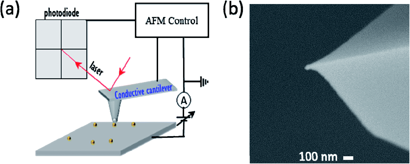 | ||
| Fig. 1 (a) The schematics of electrical measurements setup in the atomic force microscope and (b) the scanning electron microscope image of the gold-coated AFM tip used for the electrical measurements. | ||
The size and crystal structure of the NPs are accurately characterized using UV-vis method and HRTEM with atomic resolution. Fig. 2(a) shows the AFM image of well-separated Au-NPs on the n-Si substrate. The image is produced using an AFM tip with a resonance frequency of 261 kHz. The scan is carried out in the 1.4 μm × 1.4 μm region, with a scan frequency of 0.75 Hz. The sample is also characterized using SEM, as shown in Fig. 2(b), which again illustrates the individually dispersed Au-NPs. Fig. 2(c) shows the UV-visible spectroscopy of Au-NPs dispersed in citrate buffer solution. The spectrum shows the maximum absorbance peak at the wavelength of 523.5 nm, confirming the Au-NPs of size 15 nm.31,32
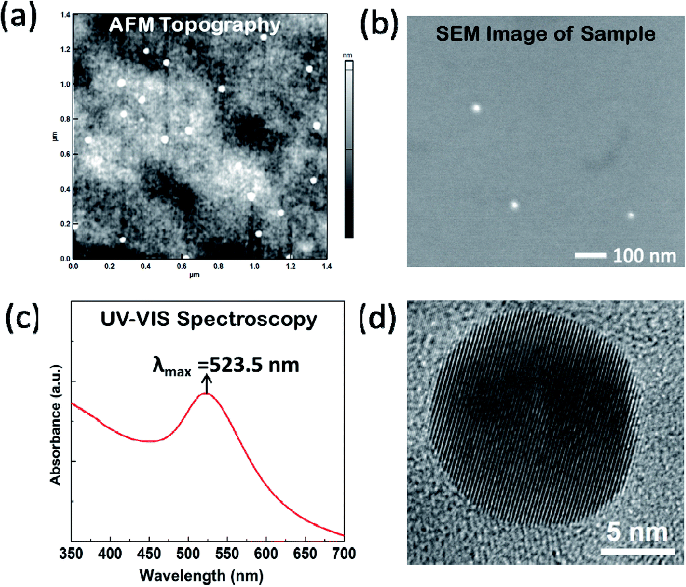 | ||
| Fig. 2 (a) The AFM topography of the sample (b) the SEM images of the nanoparticles on the n-Si substrate (c) the UV-vis spectroscopy of gold nanoparticles and (d) the investigation of nanocrystalline nature of Au-NP using high resolution (HRTEM) imaging. | ||
AFM and SEM micrographs confirm the nanoparticles are within an approximate diameter of 15 nm, and are well dispersed on the substrate. This discrete dispersion of Au-NPs is critical to investigating the electrical characteristics of the single nano-crystalline Au-NP. Fig. 2(d) shows the TEM image of Au-NP with a diameter of 14.9 nm. The crystal planes of Au-NP are shown with atomic crystal plane spacing (d-spacing) of 0.2317 nm.
The I–V measurements are carried out either on the Au-NP or directly on the n-Si substrate, using AFM nano-probe at different locations. Fig. 3 (a) and (b) shows the first and second consecutive voltage sweeps on Au-NP for the complete −2 V to +2 V sweep and 0 to +2 V sweeps respectively. Using a positive voltage sweep (reverse bias), the difference in tunneling current due to the charge trapping in Au-NP and the I–V curves is shown. On the other hand, during the negative sweeps (positive bias), the I–V curves are overlapping and the current is relatively small.
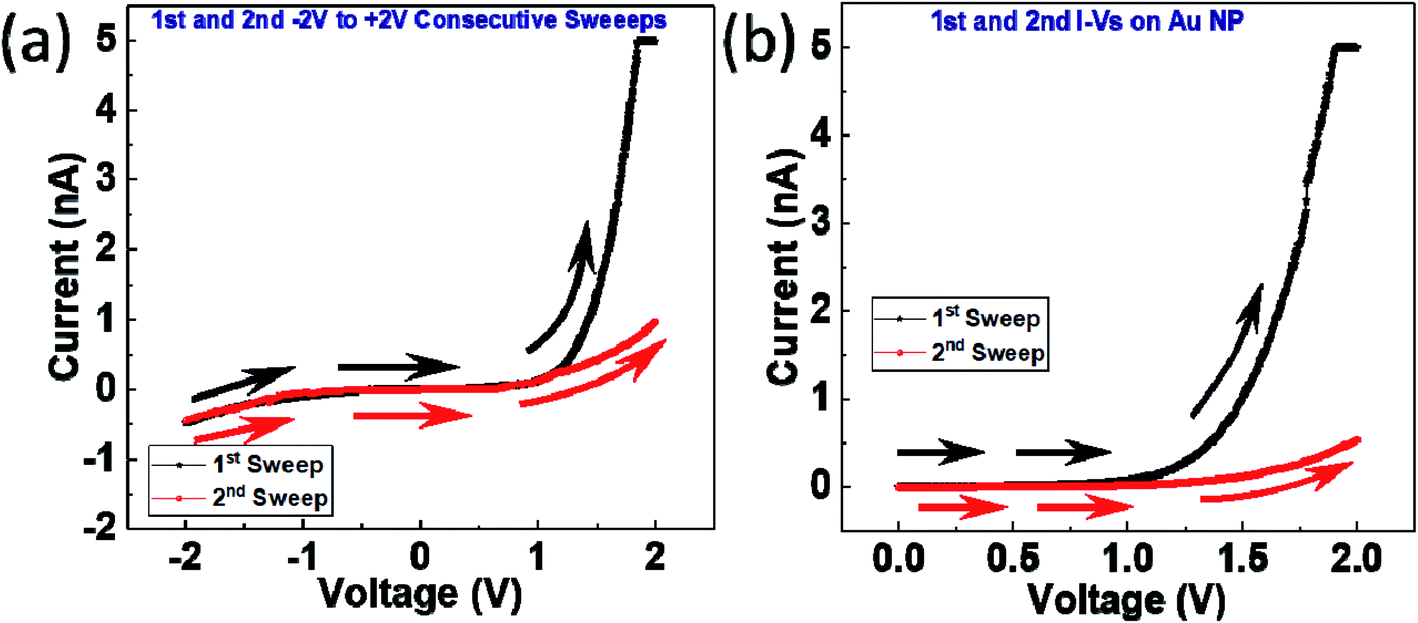 | ||
| Fig. 3 The subsequent first and second sweeps on the Au-NP (a) from −2 V to +2 V (b) from 0 to +2 V the direction of arrows shows the direction of voltage sweep. | ||
From Fig. 3 we can conclude that the tunneling current of the second sweep is smaller than that of the first sweep for voltage sweeps beyond 1.0 V. This reduction in tunneling current is attributed to the effect of charge trapped in the Au-NP during the application of first voltage sweep, which leads to a screening of the electric field at the NPs/n-Si interface.
In this work, we focus on the positive voltage (reverse bias) sweep where the tunneling current is dominant. Notably, in forward bias (negative voltage sweep) the current is very small, as shown in Fig. 3(b), due to forward conduction barrier and high contact resistance.11
Fig. 4 shows the I–V measurements of the sample when placing the AFM nano-probe directly on the n-Si surface. The (I–V) curves for consecutive positive voltage sweeps (0.0 to +2.0 V) are shown in Fig. 4, where the AFM tip is in direct contact with the n-Si substrate, and shows no change in the current during successive sweeps on n-Si substrate. It has been demonstrated that the tunneling current is a direct function of the electric field at the nano metal/Si junction, and the I–V behavior is reproducible when using the same Au AFM probe on a clean n-Si surface.12,33 Therefore, the drop in the tunneling current at the Au NP/n-Si interface at subsequent voltage sweeps, as shown Fig. 3, is a result of the reduction of the interface electric field due to the charge screening effect from the Au-NP. This effect is not observed in the absence of NPs, as shown in Fig. 4.
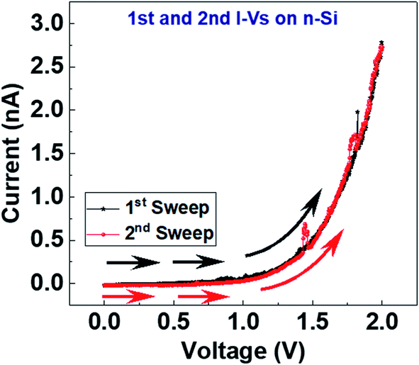 | ||
| Fig. 4 The I–V characteristics by placing tip directly on the surface and the direction of arrows show the direction of voltage sweeps. | ||
For a further understanding of the tunneling current in Fig. 3, the I–V characteristics on the Au-NP at different voltage ranges and time intervals are measured. The results showed the modulation and irreversibility of I–V curves with sequential sweeps are only observed when the probe is placed on Au-NPs. However, there is no change in I–V characteristics with multiple voltage sweeps when the AFM tip is directly in contact with the n-Si substrate, as shown in Fig. 4. To assess the impact of different voltage sweep ranges on the charge storage, different voltage sweep ranges are carried out, as shown in Fig. 5, where Fig. 5(a), (b) and (c) shows the consecutive I–V curves on Au-NPs with voltage sweeps in the range of 0 to +0.6 V, 0 to +1.0 V and 0 to +1.2 V respectively. Fig. 5(b) shows the sweeps up to +1.0 V do not pump enough charge into the Au-NP to impact the I–V characteristics, therefore, this value (+1.0 V) is considered the minimum bias to pump enough charge to create this effect. For the consecutive voltage sweep of 0 to +1.2 V we observe a slightly smaller current level as compared to that of its previous sweep as shown in Fig. 5(c). The shift in overlapping of first and second consecutive sweeps shows a small amount of charge accumulation in the Au-NP.
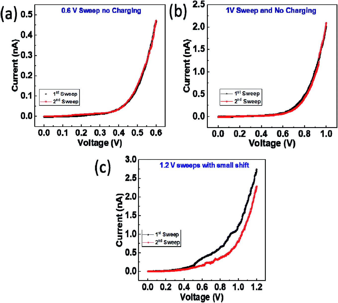 | ||
| Fig. 5 The voltage-dependent I–V measurements with (a) voltage sweep of 0–0.6 V (b) voltage Sweep of 0–1 V and (c) the sweep of 0 to 1.2 V. | ||
The time dependence of the I–V curves with a sweep range of 0 to +2.0 V, carried out at different time intervals, is shown in Fig. 6. Fig. 6(a) shows multiple I–V sweeps, with intervals (Δt) of 15 seconds (s), 30 s, 45 s and 60 s between the successive sweeps. At Δt = 60 seconds from the previous sweep, we can readily observe that the I–V curve coincides with the initial (first) I–V sweep where there was no charge stored; indicating the decay of the charge stored due to the earlier sweep.
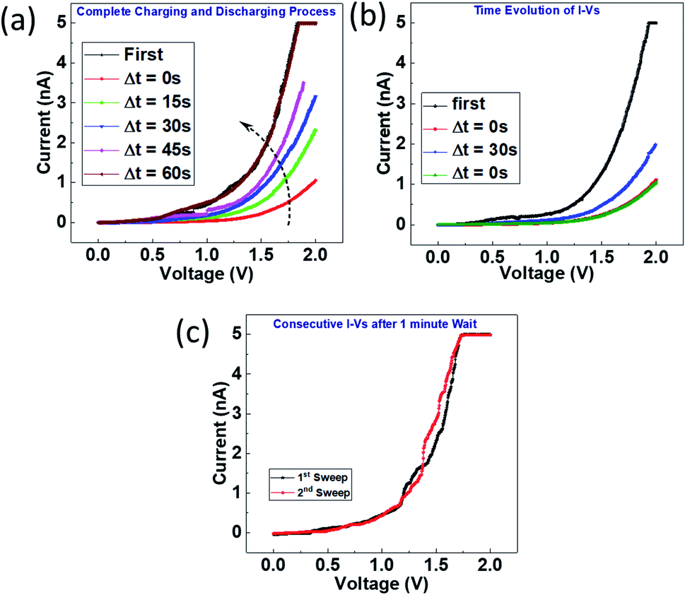 | ||
| Fig. 6 The time-dependent I–V measurements with (a) the complete charging and discharging process (b) the time-dependent voltage sweeps of 0 to +2 V (c) consecutive I–Vs with 1 minute time interval. | ||
It is worth mentioning that while each I–V measured during a sweep reads the current charge state of the Au-NP, it also injects charge into the Au-NP (if the sweep is larger than +1.0 V). Therefore, if an immediate readout sweep is carried out, a lower current state is obtained due to the charge pumping introduced by the preceding sweep. If the sweep is done after longer intervals, the charge decay states (higher I–V current) are observed and with given enough time it will get back to the non-charged state of high current. This is also captured in Fig. 6(b), which shows a different data set depicting the initial I–V curve, the immediate I–V measurement at Δt = 0 s, Δt = 30 s and again Δt = 0 s from the previous sweep. In Fig. 6(b), the immediate I–V measurement after any sweep (i.e. Δt = 0 s and after 30 s dark green color) overlaps with the lowest current level, indicating the charging effect of any full range sweep (sweep voltage >1.0 V). Fig. 6(c) shows two overlapping time-delayed I–V sweeps at the highest current, indicating no charge in the Au-NP, where the second sweep is carried out after 60 s from the first sweep. This indicates there is a charge decay time of ∼60 s. This evolution in I–V behavior can be understood considering the charge screening effect from the NPs on the current reduction in Fig. 3, as explained earlier. However, during the charge decay from the NP, the screening effect becomes less, i.e. higher electric field, hence higher tunneling current. When the NPs is completely discharged the electric field is back to the maximum value and the initial tunneling current is observed, as in Fig. 6(a) and (c).
Finally, close observation of the difference in I–V behaviors in Fig. 4 (when the AFM probe is placed directly on n-Si surface) and Fig. 3(b) (when the AFM probe is placed directly on n-Si surface), shows that charge trapping is strictly attributed to the existence of NP itself. On the other hand, if there is oxidation underneath Au NP, on Si surface, charge trapping effect will have been evident in Fig. 4 as well. Furthermore, the time evolution of the I–V curves in Fig. 6 and the restoration of the NP initial state after waiting along enough time (one minute) also supports the NP charging effect. This indicates that the effect of oxidation on n-Si underneath Au-NPs is negligible, as the n-Si is passivated with hydrogen after HF cleaning.
Conclusion
In summary, the time dependence of charge decay in individual 15 nm Au-NPs, as manifested in the I–V characteristic, is studied. The UV-visible spectroscopy, HRTEM and SEM are used to accurately confirm Au-NPs size and distribution on the substrate. The consecutive I–V measurements conducted on n-Si and Au-NP using gold-coated tip, confirmed the charging effect in the Au-NP. The results show that the irreversibility of I–V curves is a characteristic of Au-NP due to charge trapping therein. Finally, this time-dependent analysis will facilitate the use of Au-NPs for different applications in nano memory devices.Conflicts of interest
There are no conflicts to declare.Acknowledgements
This publication is based on work supported by Khalifa University of Science and Technology under Award No. CIRA-2018-21.References
- M. Homberger and U. Simon, Philos. Trans. R. Soc., A, 2010, 368, 1405–1453 CrossRef CAS.
- J.-S. Lee, Gold Bull., 2010, 43, 189–199 CrossRef.
- D. A. Giljohann, D. S. Seferos, W. L. Daniel, M. D. Massich, P. C. Patel and C. A. Mirkin, Angew. Chem., Int. Ed., 2010, 49, 3280–3294 CrossRef CAS.
- L. Dykman and N. Khlebtsov, Chem. Soc. Rev., 2012, 41, 2256–2282 RSC.
- Y. Zhang, A. Shoaib, J. Li, M. Ji, J. Liu, M. Xu, B. Tong, J. Zhang and Q. Wei, Biosens. Bioelectron., 2016, 79, 866–873 CrossRef CAS.
- A. Shoaib, M. Ji, H. Qian, J. Liu, M. Xu and J. Zhang, Nano Res., 2016, 9, 1763–1774 CrossRef CAS.
- S. Anwer, G. Bharath, S. Iqbal, H. Qian, T. Masood, K. Liao, W. J. Cantwell, J. Zhang and L. Zheng, Electrochim. Acta, 2018, 283, 1095–1104 CrossRef CAS.
- S. Iqbal, A. Bahadur, S. Anwer, S. Ali, A. Saeed, R. Muhammad Irfan, H. Li, M. Javed, M. Raheel and M. Shoaib, Appl. Surf. Sci., 2020, 526, 146691 CrossRef CAS.
- S. Iqbal, A. Bahadur, S. Anwer, M. Shoaib, G. Liu, H. Li, M. Raheel, M. Javed and B. Khalid, CrystEngComm, 2020, 22, 4162–4173 RSC.
- M. Rezeq, A. Ali, S. P. Patole, K. Eledlebi, R. K. Dey and B. Cui, AIP Adv., 2018, 8, 055122 CrossRef.
- Y. Abbas, A. Rezk, S. Anwer, I. Saadat, A. Nayfeh and M. Rezeq, Nanotechnology, 2020, 31, 125708 CrossRef CAS.
- Y. Abbas, A. Rezk, I. Saadat, A. Nayfeh and M. Rezeq, Sci. Rep., 2019, 9, 13586 CrossRef.
- W. L. Leong, P. S. Lee, S. G. Mhaisalkar, T. P. Chen and A. Dodabalapur, Appl. Phys. Lett., 2007, 90, 042906 CrossRef.
- P. Cui, S. Seo, J. Lee, L. Wang, E. Lee, M. Min and H. Lee, ACS Nano, 2011, 5, 6826–6833 CrossRef CAS.
- D. V. Talapin, J. S. Lee, M. V. Kovalenko and E. V. Shevchenko, Chem. Rev., 2010, 110(1), 389–458 CrossRef CAS.
- M. Kumar, S. Otari, H. Jeong and D. Lee, J. Alloys Compd., 2017, 725, 1115–1122 CrossRef CAS.
- Z.-C. Xu, C.-M. Shen, C.-W. Xiao, T.-Z. Yang, H.-R. Zhang, J.-Q. Li, H.-L. Li and H.-J. Gao, Nanotechnology, 2007, 18, 115608 CrossRef.
- J. Schmitt, S. Hajiw, A. Lecchi, J. Degrouard, A. Salonen, M. Impéror-Clerc and B. Pansu, J. Phys. Chem. B, 2016, 120, 5759–5766 CrossRef CAS.
- F. Liebig, A. F. Thünemann and J. Koetz, Langmuir, 2016, 32, 10928–10935 CrossRef CAS.
- M.-Y. Li, M. Sui, P. Pandey, Q. Zhang, E.-S. Kim and J. Lee, Nanoscale Res. Lett., 2015, 10, 380 CrossRef.
- J. Lee, P. Pandey, M. Sui, M.-Y. Li, Q. Zhang and S. Kunwar, Nanoscale Res. Lett., 2015, 10, 494 CrossRef.
- M. Bechelany, X. Maeder, J. Riesterer, J. Hankache, D. Lerose, S. Christiansen, J. Michler and L. Philippe, Cryst. Growth Des., 2010, 10, 587–596 CrossRef CAS.
- N. G. Bastús, J. Comenge and V. Puntes, Langmuir, 2011, 27, 11098–11105 CrossRef.
- A. Prakash, J. Ouyang, J.-L. Lin and Y. Yang, J. Appl. Phys., 2006, 100, 054309 CrossRef.
- R. J. Tseng, J. Huang, J. Ouyang, R. B. Kaner and Y. Yang, Nano Lett., 2005, 5(6), 1077–1080 CrossRef CAS.
- A. Rezk, Y. Abbas, I. Saadat, A. Nayfeh and M. Rezeq, Appl. Phys. Lett., 2020, 116, 223501 CrossRef CAS.
- G. H. Dushaq, A. Alkhatib, M. S. Rasras and A. M. Nayfeh, AIP Adv., 2015, 5, 097181 CrossRef.
- M. Rezeq, A. Ali and H. Barada, Appl. Surf. Sci., 2015, 333, 104–109 CrossRef CAS.
- M. Rezeq, C. Joachim and N. Chandrasekhar, Surf. Sci., 2009, 603, 697–702 CrossRef CAS.
- M. Rezeq, C. Joachim and N. Chandrasekhar, Microelectron. Eng., 2009, 86, 996–998 CrossRef CAS.
- V. Amendola and M. Meneghetti, J. Phys. Chem. C, 2009, 113, 4277–4285 CrossRef CAS.
- W. Haiss, N. T. K. Thanh, J. Aveyard and D. G. Fernig, Anal. Chem., 2007, 79, 4215–4221 CrossRef CAS.
- M. Rezeq, K. Eledlebi, M. Ismail, R. K. Dey and B. Cui, J. Appl. Phys., 2016, 120, 044302 CrossRef.
| This journal is © The Royal Society of Chemistry 2020 |