 Open Access Article
Creative Commons Attribution 3.0 Unported Licence
Aqueous synthesis of tin- and indium-doped WO3 films via evaporation-driven deposition and their electrochromic properties†
Hiroaki Uchiyama *a,
Yoshiki Nakamurab and
Seishirou Igarashib
aDepartment of Chemistry and Materials Engineering, Kansai University, 3-3-35 Yamate-cho, Suita, 564-8680, Japan. E-mail: h_uchi@kansai-u.ac.jp; Tel: +81-6-6368-1121 extn 6131
bKansai University, Japan
First published on 15th February 2021
Abstract
M-doped WO3 (M = Sn or In) films were prepared from aqueous coating solutions via evaporation-driven deposition during low-speed dip coating. Sn- and In-doping were easily achieved by controlling the chemical composition of simple coating solutions containing only metal salts and water. The crystallinity of the WO3, Sn-doped WO3, and In-doped WO3 films varied with heating temperature, where amorphous and crystalline films were obtained by heating at 200 and 500 °C, respectively. All the amorphous and crystalline films showed an electrochromic response, but good photoelectrochemical stability was observed only for the crystalline samples heated at 500 °C. The crystalline In–WO3 films exhibited a faster electrochromic color change than the WO3 or Sn–WO3 films, and good cycle stability for the electrochromic response in the visible wavelength region.
Introduction
Electrochromic film materials are able to reversibly change their optical properties by applying an electrical voltage, and have thus raised much attention for various practical applications, such as in smart windows, display devices, and sensor materials.1–5 Tungsten oxide (WO3) is a typically used cathodic electrochromic material because of its relatively fast color change and good stability.5–11 Two-terminal electrochromic devices based on cathodic WO3 electrodes and appropriate anodic materials such as dimethyl ferrocene,12 hydroquinone,13 tetrathiafulvalene14 (soluble anodic species), and NiO,15,16 polyaniline17 (insoluble anodic species) have been widely studied for practical applications. The electrochromic reaction of WO3 can be represented as:| WO3 + xM+ + xe− ↔ MxWO3 (M+ = H+, Li+, or Na+) |
The electrochromic performance of WO3 materials, including the response speed, the durability, and the degree of color change, is known to strongly depend on the crystallinity of the WO3 phase.5,6,18–24 The electrochromic behavior of amorphous WO3 is reported to be related to the polaron transition between W4+, W5+, and W6+ ions,18,19 and the coloration efficiency of amorphous materials is generally better than crystalline materials.5,6,20–24 However, amorphous WO3 films often dissolve in acidic electrolyte solutions, resulting in a low cycle stability.5,6,20–24 The electrochromism of crystalline WO3 can be discussed on the basis of the variation in electron density with enhanced electron scattering resulting from the intercalation of cations. Although crystalline WO3 films exhibit a high electrochemical stability and an optical modulation over a wide range of wavelengths, including the infrared region,6 the electrochromic response speed is relatively low.5,6,20,21 Therefore, controlling the crystallinity of the WO3 film material is essential for improving the electrochromic performance.
Doping with metal ions (such as Ni and Ti, among others) has been widely investigated as another strategy for making high-performance WO3 electrochromic materials.24–27 Bathe et al. investigated the influence of Ti doping on the electrochromic properties of WO3 thin films prepared by pulsed spray pyrolysis, and suggested that doping WO3 with Ti induced a phase transformation from monoclinic to amorphous and a rough surface morphology, resulting in improvement in the cycle stability, charge storage capacity, and reversibility of the films.24 Cai et al. prepared Ti-doped WO3 films with a hierarchical star-like structure by a hydrothermal method, where the star-like structure had a low charge-transfer resistance and ion diffusion resistance, leading to fast switching speed and high coloration efficiency.26 Zhou reported the preparation of Ni-doped WO3 films by a hydrothermal method, where the doping caused a distortion of the WO3 crystal structure and the formation of vertically aligned nanorods, which enhanced the optical modulation, coloration efficiency, and cycle stability.27 Such doping strategy has been also applied to other electrode materials than WO3, such as NiO. Kim et al. reported that the Cu doping into NiO films resulted in the high performance electrochromic supercapacitors.28 These results suggest that doping should allow us to achieve improvement in the electrochromic performance of WO3 materials.
In this work, we doped amorphous and crystalline WO3 films with tin (Sn4+) and indium (In3+) ions, and investigated the effect of the metal ion doping on the electrochromic properties of the WO3 films. The addition of Sn4+ or In3+ ions was expected to improve the durability of WO3 electrochromic films because these ions are electrochemically more stable than W6+ ions in aqueous media. Moreover, doping with low-valence metal ions should induce oxygen vacancies in the WO3 crystal lattice, which could influence the electron density in the WO3 phase, affecting the electrochromic performance. We recently suggested a low-speed dip-coating technique as a novel coating technique for making metal oxide thin films from organic-additive-free aqueous solutions.29–31 Fig. 1 shows a schematic illustration of the film deposition during low-speed dip coating. The evaporation-driven deposition of solutes during dip coating with extremely low substrate withdrawal speeds would hinder the aqueous solution from gathering to form droplets, achieving a homogeneous deposition of a film layer on the substrate. The evaporation-driven deposition process does not need any organic additives for modifying the wettability of the aqueous coating solutions and, thus, pure inorganic precursor layers can be obtained on a glass substrate. Such inorganic precursors, thus obtained, would enable simple control of the crystallinity of WO3 films from amorphous to crystalline by varying the heating temperature. Moreover, the aqueous route is thought to allow for the doping of WO3 materials with various metal ions because water can dissolve many different metal salts. Here, we prepared amorphous and crystalline M-doped WO3 films (M = Sn or In) by a low-speed dip-coating technique with simple aqueous solutions containing only (NH4)10W12O41·5H2O, In(NO3)3·3H2O and SnCl4·5H2O, and evaluated their electrochromic properties. The effect of Sn- and In-doping on the electrochromic performance of WO3 films was studied by measuring the cyclic voltammogram and optical modulation during electrochromic reactions.
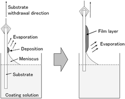 | ||
| Fig. 1 Schematic illustration of the evaporation-driven film deposition during low-speed dip coating. | ||
Experimental
Preparation of M-doped WO3 (M = Sn or In) thin films by low-speed dip coating
HCl aqueous solutions of pH 1.1–1.5 and NH3 aqueous solutions of pH 11.5 were prepared as the solvents for coating solutions by diluting with purified water ca. 36.0 mass% hydrochloric acid (Wako Pure Chemical Industries, Osaka, Japan) and ca. 10 mass% ammonia solutions (Wako Pure Chemical Industries, Osaka, Japan), respectively. Table 1 shows the compositions of the coating solutions for WO3 and M-doped WO3 (M = Sn or In) films.| Film | Coating solutions | Heat-treated films | ||||
|---|---|---|---|---|---|---|
| pH of solvents | [(NH4)10W12O41·5H2O]/mM | [SnCl4·5H2O]/mM | [InCl3·4H2O]/mM | Film thickness/nm | M (M = Sn or In)/W mole ratioa | |
| a The mole ratio was analyzed by X-ray photoelectron spectroscopy (XPS). | ||||||
| WO3 | 1.5 (HCl) | 10 | — | — | 34 | — |
| Sn–WO3 | 11.5 (NH3) | 5.0 | 6.0 | — | 35 | 0.085 |
| In–WO3 | 1.1 (HCl) | 5.0 | — | 6.0 | 38 | 0.12 |
1.25 g of (NH4)10W12O41·5H2O (Wako Pure Chemical Industries, Osaka, Japan) was added and dissolved in 40 cm3 of the HCl solutions of pH 1.5 under stirring at 60 °C. After stirring at 60 °C for 1 h, the resultant solutions served as WO3 coating solutions ([(NH4)10W12O41·5H2O] = 10.0 mM).
0.625 g of (NH4)10W12O41·5H2O and 0.0841 g of SnCl4·5H2O (Wako Pure Chemical Industries, Osaka, Japan) were added and dissolved in 40 cm3 of the NH3 solutions of pH 11.5 under stirring at 60 °C. After stirring at 60 °C for 1 h, the solutions served as Sn-doped WO3 (Sn–WO3) coating solutions ([(NH4)10W12O41·5H2O] = 5.00 mM, [SnCl4·5H2O] = 6.00 mM, and the Sn/W mole ratio was 0.1).
0.625 g of (NH4)10W12O41·5H2O and 0.0704 g of In(NO3)3·4H2O (Wako Pure Chemical Industries, Osaka, Japan) were added and dissolved in 40 cm3 of the HCl solutions of pH 1.1 under stirring at 60 °C. After stirring at 60 °C for 1 h, the solutions served as In-doped WO3 (In–WO3) coating solutions ([(NH4)10W12O41·5H2O] = 5.00 mM, [In(NO3)3·4H2O] = 6.00 mM, and the In/W mole ratio was 0.1).
WO3 and M-doped WO3 (M = Sn or In) precursor films were deposited on fluorine-doped tin oxide (FTO) glass substrates (20 mm × 40 mm × 1.0 mm) by a low-speed dip-coating technique. Low-speed dip coating was performed using a dip-coater (Portable Dip Coater DT-0001, SDI, Kyoto, Japan) in a thermostatic oven, where the substrates were withdrawn at 0.05 cm min−1. The coating temperature, i.e., the temperature of the substrates, solutions, and atmosphere, was kept at 25 °C (for In-doped WO3 films) or 40 °C (for WO3 and Sn-doped WO3 films), where the solutions and substrates were heated at the prescribed temperature for 10 min in the thermostatic oven before the dip coating. The precursor films were heated in air at 200 °C for 24 h or at 500 °C for 0.5 h, where the precursor films were directly transferred to an electric furnace held at the prescribed temperature. Hereafter, the Sn- and In-doped WO3 films are denoted as Sn– and In–WO3 films.
Characterization
Microscopic observation of the thin film samples was carried out using an optical microscope (KH-1300, HiROX, Tokyo, Japan). The microstructure of the thin films was observed using a field emission scanning electron microscope (FE-SEM; Model JSM-6500F, JEOL, Tokyo, Japan). The crystalline phases were identified using an X-ray diffractometer (Model Rint-Ultima III, Rigaku, Tokyo, Japan) with CuKα radiation operated at 40 kV and 40 mA at an incident angle of 0.5°. The chemical compositions of the product films were obtained using an X-ray photoelectron spectrometer (XPS; PHI5000 Versa Probe, ULVAC-PHI, Chigasaki, Japan) with a monochromatic AlKα X-ray source. The XPS analysis was done for the film samples coated on silica glass substrates, because FTO substrates containing Sn4+ ions inhibited the analysis of Sn–WO3 films. To counter the surface charging, a charge neutralizer was used during the collection of the spectra.Film thickness was measured using a contact probe surface profilometer (SE-3500K31, Kosaka Laboratory, Tokyo, Japan). A part of the thin film was scraped off with a surgical knife immediately after the film deposition, and the level difference between the coated part and the scraped part was measured after heat treatment.
Measurement of electrochromic properties
Electrochromic properties of the WO3 and M-doped WO3 films were evaluated at room temperature in a three-electrode cell using a potentiostat (HZ-7000, Hokuto Denko, Osaka, Japan) consisting of the film sample, a platinized Pt electrode, and a saturated calomel electrode (SCE) as the working, counter, and reference electrodes, respectively. An aqueous solution of 1 M H2SO4 was used as the supporting electrolyte.Cyclic voltammetry (CV) was performed on the WO3 and M-doped WO3 films at a scan rate of 10 mV s−1 between −1.0 and 2.0 V vs. the SCE.
The optical modulation induced by electrochromic reactions was evaluated by an in situ optical absorption measurement. The three-electrode cell with circular silica windows (1.77 cm2) as a light path for an in situ UV-Vis-NIR absorption measurement was connected to a potentiostat, and set in the optical spectrometer (V-570, JASCO, Tokyo, Japan). The coloring and bleaching of the WO3 and M-doped WO3 films was carried out at −0.75 and 1.5 V vs. the SCE, respectively. The application of voltage was stopped at 5- (coloring) or 100- (bleaching) second intervals, and then optical absorption spectra were measured at wavelengths of 300–1300 nm. An FTO glass substrate was used as the reference for the optical measurement. Coloring and bleaching times were defined as the times when the variation in the optical absorption spectra stopped moving upon application of a voltage.
The cycle stability was tested by repeating the electrochromic color change. The coloring and bleaching cycles were repeated 50 times, where the coloring and bleaching of the films were performed by a voltage application of −0.75 V vs. the SCE for 20 s and 1.5 V vs. the SCE for 200 s, respectively. After 1 and 50 cycles, the optical absorption spectra of the film samples were measured.
Results and discussion
Preparation and characterization of WO3 and M-doped WO3 (M = Sn or In) films
Coating solutions for the WO3 and In–WO3 films were prepared with HCl solutions of pH 1.5 and 1.1, respectively. However, coating solutions containing SnCl4 became cloudy under acidic conditions because of precipitate formation. Transparent coating solutions for Sn–WO3 films were obtained under alkaline conditions with NH3 solutions of pH 11.5. Precursor films were deposited on FTO glass substrates by low-speed dip coating, and then heated at 200 °C for 24 h or at 500 °C for 0.5 h for the thermal conversion to WO3, Sn–WO3, and In–WO3 films. Fig. 2 shows optical micrographs of the WO3, Sn–WO3, and In–WO3 films heated at 500 °C. All the product films were free from cracks and had a high level of transparency. In this work, we prepared Sn–WO3 and In–WO3 films with a wide range of M/W mole ratios (M = Sn or In) between 0.050 and 0.20. However, the Sn–WO3 films became cloudy when the Sn/W mole ratio was over 0.10, which may be because of the generation of SnO2 phase in the films. Therefore, the M/W mole ratio was fixed at 0.10 and these results are discussed hereafter. The thickness and the M/W (M = Sn or In) mole ratio of the product films heated at 500 °C are shown in Table 1. The film thickness was ca. 35 nm irrespective of whether doping was with Sn4+ or In3+ ions. The M/W mole ratios (M = Sn or In) in the Sn–WO3 and In–WO3 films, as evaluated by XPS, were 0.085 and 0.12, respectively, which closely agree with the compositions of the coating solutions (0.10) (the XPS spectra are shown in ESI Fig. S1†). In this work, low-concentration (NH4)10W12O41 aqueous solutions were used as the coating solutions ([(NH4)10W12O41·5H2O] = 5.00 or 10.0 mM) because tungsten salts are poorly soluble in many different solvents containing water and alcohols. However, homogeneous coating on the whole substrates was achieved with the low-concentration solutions via one-time coating. In the case of low-speed dip coating, the solvent preferentially evaporates at the edge of the meniscus, and the coating solutions are then locally concentrated there, resulting in the deposition of solutes on the substrates (Fig. 1).29–31 The evaporation-induced concentration enabled us to make homogeneous WO3 coating layers even from low-concentration solutions. Moreover, in this process, Sn- or In-doping was easily succeeded by the addition of tin or indium salts into the coating solutions.XRD patterns of the WO3, Sn–WO3, and In–WO3 films heated at 200 and 500 °C are shown in Fig. 3 and 4, respectively. Any diffraction peaks other than those due to FTO substrates were not observed for the WO3, Sn–WO3, or In–WO3 films heated at 200 °C (Fig. 3), which indicates that the films heated at this temperature consisted of an amorphous phase. Diffraction patterns attributable to the monoclinic WO3 phase appeared for all the films heated at 500 °C (Fig. 4), where SnO2 or In2O3 phases were not detected in the Sn–WO3 or In–WO3 films, respectively. The peak shift due to the substitution of Sn4+ or In3+ ions for W6+ ions was not clearly observed in the XRD patterns of the Sn–WO3 or In–WO3 films, while the diffraction peaks of the (002), (020), and (200) planes of monoclinic WO3 weakened and broadened upon the addition of Sn4+ and In3+ ions, which suggests that Sn- or In-doping could result in deformation of the WO3 lattice.
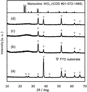 | ||
| Fig. 3 XRD patterns of the FTO substrate (a), and the WO3 (b), Sn–WO3 (c), and In–WO3 (d) films heated at 200 °C. | ||
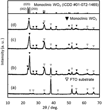 | ||
| Fig. 4 XRD patterns of the FTO substrate (a), and the WO3 (b), Sn–WO3 (c), and In–WO3 (d) films heated at 500 °C. | ||
Electrochromic properties of WO3 and M-doped WO3 (M = Sn or In) films
The electrochromic properties were evaluated for the amorphous and crystalline WO3, Sn–WO3, and In–WO3 films heated at 200 and 500 °C, respectively, where the electrochemical measurements were performed in an aqueous electrolyte of 1 M H2SO4. In this case, the coloring and bleaching of WO3 films progressed with the intercalation and deintercalation of H+ ions. The coloring of WO3 films is the following reduction reaction:5| WO3 + H+ + e− → HWO3 (deep blue color). |
The bleaching of the films then follows the oxidation reaction:
| HWO3 → WO3 + H+ + e− (light yellow color). |
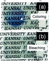
Fig. 5 shows cyclic voltammograms obtained for the amorphous and crystalline product films. Cathodic peaks from the reduction reaction with H+ ions were detected between −0.65 and −1.0 V vs. the SCE, irrespective of the heating temperature or the metal ion dopant used (Fig. 5), where the coloring of the films to deep blue was visually confirmed for all the films (see Fig. 6a). The cathodic response was almost unchanged with the variation in the crystallinity and the addition of Sn4+ or In3+ ions (Fig. 5). The anodic response due to the oxidation reaction was observed between −0.50 and 0.30 V vs. the SCE in the CV curves for all the films, and the bleaching of the blue color started there (Fig. 6b). The anodic peaks in the CV curves broadened with a decrease in heating temperature (Fig. 5), and the amorphous WO3, Sn–WO3, and In–WO3 films heated at 200 °C were partially dissolved after the coloring and bleaching cycle (Fig. 7a). Such dissolution of the films was not observed for the crystalline films heated at 500 °C (Fig. 7b). These results could indicate that the electrochemical stability of the amorphous films was relatively low, and the Sn- and In-doping did not improve the durability of the amorphous WO3 films. Therefore, hereafter, we mainly focused on the effect of the Sn- and In-doping on the electrochromic response of the crystalline WO3, Sn–WO3, and In–WO3 films heated at 500 °C.
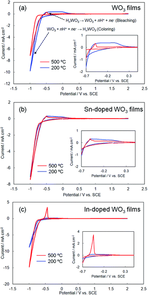 | ||
| Fig. 5 Cyclic voltammograms of the WO3 (a), Sn–WO3 (b), and In–WO3 (c) films heated at 200 and 500 °C. | ||
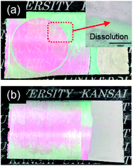 | ||
| Fig. 7 Optical micrographs of the amorphous (a) and crystalline (b) In–WO3 films after the coloring and bleaching cycle. | ||
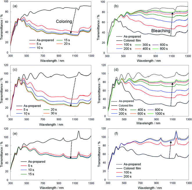
We evaluated the response speed of the electrochromic optical modulation for the crystalline WO3, Sn–WO3, and In–WO3 films, where the UV-Vis-NIR absorption spectra were measured when a voltage was applied. The coloring and bleaching of the films were carried out at −0.75 and 1.5 V vs. the SCE, respectively. Fig. 8 shows the variation in the UV-Vis-NIR absorption spectra of the crystalline WO3 (Fig. 8a and b), Sn–WO3 (Fig. 8c and d), and In–WO3 (Fig. 8e and f) films upon application of a voltage, and Table 2 shows the reaction time that was needed to finish the coloring and breaching of the films. The transmittance of the as-prepared crystalline WO3, Sn–WO3, and In–WO3 films was over 80% at wavelengths of 500–1300 nm (Fig. 8). The transmittance of the films decreased with the coloring by applying −0.75 V vs. the SCE. The coloring of the films concluded within 20 s for all the crystalline films, where the transmittance of WO3, Sn–WO3, and In–WO3 films at wavelengths greater than 600 nm was reduced to ca. 30, 20, and 40%, respectively (Fig. 8a, c, e and Table 2). The bleaching of the films was achieved by applying 1.5 V vs. the SCE. The crystalline WO3 and Sn–WO3 films needed around 800 s for bleaching, where the transmittance was not completely returned to that of the as-prepared state (Fig. 8b, d and Table 2). However, the blue color of the In–WO3 films rapidly bleached within 200 s, and the transparency almost completely returned to the as-prepared state (Fig. 8f and Table 2). Although the initial transmittance of colored In–WO3 films was relatively high (ca. 40%) (Fig. 8e), the response of the In–WO3 films was obviously faster than those of the WO3 and Sn–WO3 films. To our knowledge, the improvement in the electrochromic properties of WO3 materials by doping with In3+ ions has not been reported previously.
| Film | Coloring time/s | Bleaching time/s |
|---|---|---|
| WO3 | 15 | 800 |
| Sn–WO3 | 20 | 800 |
| In–WO3 | 10 | 200 |
The response speed of electrochromic materials is influenced by several factors, such as the porosity, crystallinity, and electron conductivity, among other factors. Because electrochemical reactions occur on the surface of electrode materials, the microstructures of the WO3 films can affect the electrochromic properties. However, there were no significant differences in the surface structures, as observed by FE-SEM, between the WO3, Sn–WO3, and In–WO3 films (ESI Fig. S2†). Disorder in the WO3 crystal lattice is also known to improve the electrochromic response because the resulting broadened channels can allow for smoother insertion of cations (such as H+ and Li+). Many researchers have reported that metal ion doping deformed the monoclinic structure of WO3 materials, providing faster electrochromic reactions.24,26,27 In the present work, Sn- and In-doping caused deformation of the WO3 lattice (Fig. 4). Thus, the improvement of response speed by In-doping was thought to be influenced by the deformation of the WO3 lattice (Fig. 4). However, the Sn-doping did not provide such a fast electrochromic response (Fig. 8c, d and Table 2), despite the lattice deformation. The difference in the effect on the electrochromic properties between the Sn- and In-doped materials might be caused by the difference in valence of the Sn4+ versus In3+ ions. For crystalline WO3 materials, electrochromism is discussed on the basis of the variation in electron density with enhanced electron scattering from the intercalation of cations.5 The addition of In3+ ions might provide more oxygen vacancies than would Sn4+ ions, affecting the electrochromic behavior. To investigate the effect of the dopants, we attempted to investigate the valence states of W, In, and Sn elements in colored and bleached films by XPS. However, the thickness of the Sn–WO3 and In–WO3 films was very thin (ca. 35 nm) and the Sn and In contents were not sufficiently high (the Sn or In/W mole ratios were ca. 0.1). Thus, the surface impurities and the FTO substrates containing Sn4+ ions inhibited the precise analysis of the In and Sn elements, and consequently the difference in the valence states could not be adequately evaluated here. Detailed analysis of the valence states of Sn–WO3 and In–WO3 films remains a challenge.
Finally, we evaluated the cycle stability of crystalline In–WO3 films by repeating the coloring and bleaching. Fig. 9 shows UV-Vis-NIR absorption spectra of the crystalline In–WO3 films after 1 and 50 electrochromic cycles. The degree of coloring was maintained in the visible and near-infrared regions even after 50 cycles (Fig. 9). On the other hand, the transparency of the bleached states did not completely return to the as-prepared state in the near-infrared range over 800 nm after 50 cycles (Fig. 9). However, the bleached films after 50 cycles exhibited sufficiently high transmittance (over 80%) in the visible wavelength range between 400 and 800 nm (Fig. 9). These results show that the crystalline In–WO3 films have good cycle stability for use in electrochromic devices working at visible wavelengths.
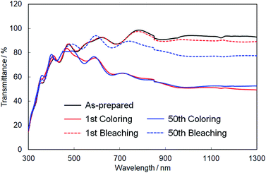 | ||
| Fig. 9 UV-Vis-NIR absorption spectra of the crystalline In–WO3 films after 1 and 50 electrochromic cycles. | ||
Conclusions
WO3 and M-doped WO3 (M = Sn or In) electrochromic films were obtained from aqueous solutions containing (NH4)10W12O41·5H2O, In(NO3)3·3H2O and SnCl4·5H2O by a low-speed dip-coating technique. Evaporation-driven deposition during low-speed dip coating enabled us to make homogeneous coating layers, even from low-concentration aqueous solutions. The Sn- and In-doping were easily achieved by controlling the chemical compositions of the solutions. The crystallinity of the WO3, Sn–WO3, and In–WO3 films was controlled by varying the heating temperature. The crystalline films heated at 500 °C showed high electrochemical stability, while the amorphous films obtained by heating at 200 °C dissolved after the electrochromic reactions. The crystalline In–WO3 films exhibited a faster coloring and bleaching response than did the WO3 and Sn–WO3 films, and this may be because of lattice deformation of the monoclinic WO3 phase and the change in valence states of the elements resulting from the In-doping. The crystalline In–WO3 films showed good cycle stability at visible wavelengths and are thus expected to be able to be applied to electrochromic devices.Conflicts of interest
There are no conflicts to declare.Acknowledgements
This work was supported by KAKENHI, Grant-in-Aid for Scientific Research (C), Grant Number JP19K05660. We thank Iain Mackie, PhD, from Edanz Group (https://en-author-services.edanzgroup.com/ac) for editing a draft of this manuscript.References
- J. Livage and D. Ganguli, Sol. Energy Mater. Sol. Cells, 2001, 68, 365–381 CrossRef CAS.
- R. J. Mortimer, Chem. Soc. Rev., 1997, 26, 147–156 RSC.
- G. A. Niklasson and C. G. Granqvist, J. Mater. Chem., 2007, 17, 127–156 RSC.
- P. R. Somani and S. Radhakrishnan, Mater. Chem. Phys., 2003, 77, 117–133 CrossRef CAS.
- D. T. Gillaspie, R. C. Tenent and A. C. Dillon, J. Mater. Chem., 2010, 20, 9585–9592 RSC.
- H. D. Zheng, J. Z. Ou, M. S. Strano, R. B. Kaner, A. Mitchell and K. Kalantar-Zadeh, Adv. Funct. Mater., 2011, 21, 2175–2196 CrossRef CAS.
- S. H. Lee, R. Deshpande, P. A. Parilla, K. M. Jones, B. To, A. H. Mahan and A. C. Dillon, Adv. Mater., 2006, 18, 763–766 CrossRef CAS.
- A. Rougier, F. Portemer, A. Quede and M. El Marssi, Appl. Surf. Sci., 1999, 153, 1–9 CrossRef CAS.
- C. Santato, M. Odziemkowski, M. Ulmann and J. Augustynski, J. Am. Chem. Soc., 2001, 123, 10639–10649 CrossRef CAS.
- T. D. Nguyen, L. P. Yeo, D. Mandler, S. Magdassi and A. L. Y. Tok, RSC Adv., 2019, 9, 16730–16737 RSC.
- T. D. Nguyen, L. P. Yeo, A. J. Ong, W. Zhiwei, D. Mandler, S. Magdassi and A. L. Y. Tok, Mater. Today Energy, 2020, 18, 100496 CrossRef.
- T. Y. Yun, X. Li, J. Bae, S. H. Kim and H. C. Moon, Mater. Des., 2019, 162, 45–51 CrossRef CAS.
- T. Y. Yun, X. Li, S. H. Kim and H. C. Moon, ACS Appl. Mater. Interfaces, 2018, 10, 43993–43999 CrossRef CAS.
- Y. M. Kim, X. Li, K. Kim, S. H. Kim and H. C. Moon, RSC Adv., 2019, 9, 19450–19456 RSC.
- J. Zhang, J. P. Tu, X. H. Xia, Y. Qiao and Y. Liu, Sol. Energy Mater. Sol. Cells, 2009, 93, 1840–1845 CrossRef CAS.
- K. Kim, T. Y. Yun, S. You, X. Tang, J. Lee, Y. Seo, Y. Kim, S. H. Kim, H. C. Moon and J. K. Kim, NPG Asia Mater., 2020, 12, 84 CrossRef CAS.
- W. Wang, X. Wang, X. Xia, Z. Yao, Y. Zhang and J. Tu, Nanoscale, 2018, 10, 8162–8169 RSC.
- E. Ozkan, S. H. Lee, C. E. Tracy, J. R. Pitts and S. K. Deb, Sol. Energy Mater. Sol. Cells, 2003, 79, 439–448 CrossRef CAS.
- Y. Liu, G. Z. Yuan, C. Z. Hua, Y. X. Zhang, G. R. Han and H. Jiang, ECS J. Solid State Sci. Technol., 2019, 8, P1–P6 CrossRef CAS.
- M. Deepa, A. K. Srivastava and S. A. Agnihotry, Acta Mater., 2006, 54, 4583–4595 CrossRef CAS.
- J. M. Wang, E. Khoo, P. S. Lee and J. Ma, J. Phys. Chem. C, 2008, 112, 14306–14312 CrossRef CAS.
- R. Giannuzzi, M. Balandeh, A. Mezzetti, L. Meda, P. Pattathil, G. Gigli, F. D. Fonzo and M. Manca, Adv. Opt. Mater., 2015, 3, 1614–1622 Search PubMed.
- W. Cheng, J. He, K. E. Dettelbath, N. J. J. Johnson, R. S. Sherbo and C. P. Berlinguette, Chem, 2018, 4, 821–832 CAS.
- S. R. Bathe and P. S. Patil, Solid State Ionics, 2008, 179, 314–323 CrossRef CAS.
- H. J. Ahn, H. S. Shim, Y. E. Sung, T. Y. Seong and W. B. Kim, Electrochem. Solid-State Lett., 2007, 10, E27–E30 CrossRef CAS.
- G. F. Cai, X. L. Wang, D. Zhou, J. H. Zhang, Q. Q. Xiong, C. D. Gu and J. P. Tu, RSC Adv., 2013, 3, 6896–6905 RSC.
- J. L. Zhou, Y. X. Wei, G. Luo, J. M. Zheng and C. Y. Xu, J. Mater. Chem. C, 2016, 4, 1613–1622 RSC.
- S. M. Kim, T. Y. Yun, K. S. Yu and H. C. Moon, ACS Appl. Mater. Interfaces, 2020, 12, 51978–51986 CrossRef CAS.
- T. Ito, H. Uchiyama and H. Kozuka, Langmuir, 2017, 33, 5314–5320 CrossRef CAS.
- H. Uchiyama, S. Igarashi and H. Kozuka, Langmuir, 2016, 32, 3116–3121 CrossRef CAS.
- H. Uchiyama, T. Ito, R. Sasaki and H. Kozuka, RSC Adv., 2015, 5, 20371–20375 RSC.
Footnote |
| † Electronic supplementary information (ESI) available. See DOI: 10.1039/d1ra00125f |
| This journal is © The Royal Society of Chemistry 2021 |

