 Open Access Article
Creative Commons Attribution 3.0 Unported Licence
Comment on “Improving the efficiency of a CIGS solar cell to above 31% with Sb2S3 as a new BSF: a numerical simulation approach by SCAPS-1D” by M. F. Rahman and S. Goumri-Said et al., RSC Adv., 2024, 14, 1924
Alexander P. Kirk
Central R&D LLC, Schaumburg, IL 60194, USA. E-mail: apkirk88@gmail.com
First published on 7th October 2024
Abstract
It was reported in early 2024 that a single-junction 1.1 eV bandgap copper indium gallium selenide (CIGS) solar cell can achieve actual power conversion efficiency up to 40.70%, open circuit voltage up to 1.330 V, and fill factor up to 90.55% at 300 K when the solar cell is irradiated by the air mass 1.5 global (AM1.5G) solar spectrum (M. F. Rahman et al., RSC Adv., 2024, 14, 1924–1938). These simulated solar cell performance parameters exceed the ideal detailed balance-limiting power conversion efficiency, open circuit voltage, and fill factor of a 1.1 eV bandgap single-junction solar cell.
1 Introduction
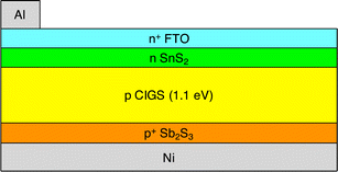
Based on simulations run with a conventional one-dimensional drift-diffusion solar cell modeling program, SCAPS-1D, Rahman et al. reported that a conventional 1.1 eV bandgap copper indium gallium selenide (CIGS) solar cell can achieve actual air mass 1.5 global (AM1.5G) power conversion efficiency η up to 40.70%, open circuit voltage Voc up to 1.330 V, and fill factor FF up to 90.55%.1 The device design that was simulated contains an aluminum (Al) top grid contact, a 50 nm thick fluorine-doped tin oxide (FTO) layer, a 50 nm thick tin disulfide (SnS2) layer, a 1.1 eV bandgap CIGS primary absorbing layer with thickness up to 3000 nm, a 200 nm thick antimony trisulfide (Sb2S3) layer, and a nickel (Ni) rear contact. A schematic of the solar cell proposed by Rahman et al. is shown in Fig. 1.2 Discussion
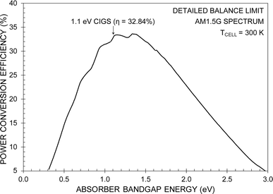
Before modeling any type of solar cell with a standard drift-diffusion computer program, it is helpful to determine its theoretical efficiency limit. In the field of photovoltaics, this is typically accomplished by using the principle of detailed balance to calculate the ideal limiting efficiency.2,3 The benefit of this approach is that the detailed balance formalism allows for a fundamental determination of the efficiency limit of a solar cell independent of specific device design features such as the thickness of individual layers, the dopant concentrations, and the contact metal work functions. Moreover, the only sink for photogenerated electron and hole recombination at steady-state and open circuit is the necessary radiative recombination whereas the undesirable nonradiative Auger and Shockley–Read–Hall recombination are not considered. A plot of the detailed balance-limiting power conversion efficiency η of single-junction solar cells, as a function of absorber bandgap energy, is shown in Fig. 2.The equations required to calculate the detailed balance-limiting performance are listed next. The open circuit voltage is expressed as Voc = Eg/q − (kT/q)ln[(2πqEg2kT)/(h3c2Jsc)], where Eg is the bandgap energy, q is the electron charge, k is the Boltzmann constant, T is the cell temperature, h is the Planck constant, and c is the speed of light in vacuum. The max power point voltage is expressed as Vmp ≈ Voc − (kT/q)ln[1 + (qVoc/kT)]. The max power point current density is expressed as Jmp = Jsc/[1 + (kT/qVmp)]. The fill factor is expressed as FF = (JmpVmp)/(JscVoc). The power conversion efficiency is expressed as η = Pout/Pin, where Pout = JmpVmp and Pin = 0.1 W cm−2 (AM1.5G irradiance).
The maximum available short circuit current density Jsc of a 1.1 eV bandgap semiconductor is 44.23 mA cm−2 when considering the AM1.5G solar spectrum. In Table 1, the detailed balance-limiting Voc, FF, and η are shown for two cases. In Case 1, the maximum AM1.5G spectrum Jsc of 44.23 mA cm−2 is considered. In Case 2, a reduced Jsc of 34.55 mA cm−2 is considered. This smaller Jsc value was chosen to match the peak Jsc reported by Rahman et al.1 Nonetheless, in both cases the detailed balance-limiting Voc, FF, and η are less than the peak values reported by Rahman et al.1 In particular, refer to the simulated Voc, FF, and η values reported in Section 4.3 on p. 1932 as well as Fig. 4 on p. 1929, Fig. 6 on p. 1931, and Fig. 7 on p. 1932 of the article by Rahman et al.1 Not only do these figures show simulated peak Voc, FF, and η exceeding the ideal detailed balance limit, they also show that these simulated peak performance parameters occur when the bulk and interface defect concentrations are the largest of the range of values that were simulated by Rahman et al.1 Note, too, that the peak Voc (1.330 V) reported by Rahman et al. exceeds the bandgap-equivalent voltage (Eg/q = 1.1 V) of the CIGS absorber.
| Case | Absorber | Eg (eV) | Jsc (mA cm−2) | Voc (V) | Vmp (V) | Jmp (mA cm−2) | FF (%) | η (%) |
|---|---|---|---|---|---|---|---|---|
| a Key: Eg is bandgap energy, Jsc is short circuit current density, Voc is open circuit voltage, Vmp is max power point voltage, Jmp is max power point current density, FF is fill factor, and η is power conversion efficiency. Note: “Case 1” assumes maximum AM1.5G Jsc whereas “Case 2” assumes a reduced Jsc. Note: Rahman et al. reported Voc up to 1.330 V, FF up to 90.55%, and η up to 40.70%. | ||||||||
| 1 | CIGS | 1.1 | 44.23 | 0.8590 | 0.7676 | 42.79 | 86.46 | 32.84 |
| 2 | CIGS | 1.1 | 34.55 | 0.8526 | 0.7614 | 33.42 | 86.38 | 25.44 |
3 Conclusion
In summary, Rahman et al. reported unrealistic values of open circuit voltage Voc, fill factor FF, and power conversion efficiency η of a 1.1 eV CIGS single-junction solar cell even though their proposed solar cell is a conventional device that was modeled with standard drift-diffusion physics. More to the point, in their device simulations, Rahman et al. did not consider hot carrier collection or some other attribute that might result in actual open circuit voltage and power conversion efficiency exceeding the detailed balance-limiting open circuit voltage and power conversion efficiency.Author contributions
Alexander P. Kirk: conceptualization, formal analysis, visualization, writing – original draft, review & editing.Conflicts of interest
There are no conflicts of interest to declare.References
- M. F. Rahman, M. Chowdhury, L. Marasamy, M. K. A. Mohammed, M. D. Haque, S. R. A. Ahmed, A. Irfan, A. R. Chaudhry and S. Goumri-Said, Improving the efficiency of a CIGS solar cell to above 31% with Sb2S3 as a new BSF: a numerical simulation approach by SCAPS-1D, RSC Adv., 2024, 14, 1924–1938 RSC.
- W. Shockley and H. J. Queisser, Detailed balance limit of efficiency of p–n junction solar cells, J. Appl. Phys., 1961, 32, 510–519 CrossRef CAS.
- C. H. Henry, Limiting efficiencies of ideal single and multiple energy gap terrestrial solar cells, J. Appl. Phys., 1980, 51, 4494–4500 CrossRef CAS.
| This journal is © The Royal Society of Chemistry 2024 |


